I. INTRODUCTION
The solar electricity including solar photovoltaics (PV) is expected to contribute as the main energy with a share of about 20% and 70% in 2050 and 2100, respectively in total energy of the world, according to the recommendation (World Energy Vision 2100) by the German Advisory Council on Global Change. 1 The Fukushima nuclear power plant accident occurred in March 2011 has given us very important messages such as unclearness for safety and cost effectiveness of nuclear energy and important of clean renewable energies including PV instead of nuclear energy. These suggest importance of further development of science and technology of PV and international collaboration and cooperation for PV.
A R&D program of PV power generation systems in Japan was started as part of a national program called the “Sunshine Project” in 1974 and it continues today. As results of continuous research development of PV since 1974, roof-top program since 1994 and feed-in-tariff program since 2012, cumulative PV system installation in Japan reached about 42GW in 2016. The cumulative PV system installation by 2030 in Japan is 100GW under the NEDO’s PV2030 Roadmap. Reference Kurokawa, Kawasaki and Ito2 For this end, further development of science, technology, and deployment of PV is necessary. This article overviews PV R&D projects in Japan as the Project Leader of the Project “High Performance Photovoltaic System Technology Development for the Future” under the New Energy and Industrial Technology Development Organization (NEDO) and the Research Supervisor of the Research Area “Creative Clean Energy Generation by using Solar Energy” under the Japan Science and Technology Agency (JST).
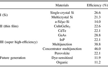
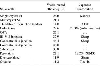
Table I shows the present status of various types of solar cells as a measure of current conversion efficiency achieved. Various solar cells and materials have great potential as major solar cells and materials including single-crystalline Si, III–V multijunction cells, CIGSe, and CdTe cells are expected to have great potential of space and terrestrial application because of high-efficiency, light-weight, and low-cost potential. However, there are some problems to be solved for further development of high-efficiency solar cells. Because point defects even in crystalline Si, dislocations, and interface recombination in CIGSe and CdTe solar cell materials affect solar cell properties, understanding and controlling those defects are very important for realizing higher efficiency. This article presents analytical results for high-efficiency potential of single-crystalline Si solar cells, GaAs, and III–V compound 3- and 5-junction cells, CIGSe and CdTe solar cells.
Present status of various types of solar cells as a measure of current conversion efficiency achieved at laboratories.

II. OVERVIEW OF R&D ACTIVITIES UNDER THE NEDO AND JST PV R&D PROGRAMS
This section overviews PV R&D projects in Japan as the Project Leader of the Project “High Performance Photovoltaic System Technology Development for the Future” under the NEDO and the Research Supervisor of the Research Area “Creative Clean Energy Generation by using Solar Energy” under the JST.
A. NEDO’s short-term project “high performance PV generation system for the future”
Further development in increasing conversion efficiency, reducing cost, and improving reliability and so forth is necessary for deployment of PV. Under the NEDO PV R&D Project called with “High Performance PV Generation System for the Future”, solar cell module efficiency targets for crystalline Si, thin-film Si, CIGS, and dye/organic were 20%, 14%, 18%, and 10%, respectively. In addition, targets of electricity cost and module cost by 2017 are 14JPY/kW h and 40JPY/W, respectively.
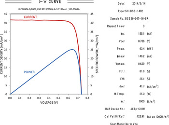
Under this project, 25.1% (V oc = 736 mV, J sc = 41.7 mA/cm2, FF = 81.9%; V oc = 729 mV, J sc = 42.0 mA/cm2, FF = 82.0%) efficiency has been demonstrated with 19.3 × 19.3 mm area, 150 μm thick heterojunction back-contact (HBC) crystalline Si solar cells by Sharp Reference Nakamura, Asano, Hieda, Okamoto, Ohnishi, Kobayashi, Tadokoro, Suganuma, Matsumoto, Katayama, Higashi, Kamikawa, Kimoto, Harada, Sakai, Shigeta, Kuniyoshi, Tsujino, Zou, Koide and Nakamura3 as shown in Figs. 1 and 2. Further improvements by improving passivation, understanding interface, device modeling, and optimum design will be made.
A structure of HBC crystalline Si solar cell developed by Sharp Co. (adapted with permission from Ref. Reference Nakamura, Asano, Hieda, Okamoto, Ohnishi, Kobayashi, Tadokoro, Suganuma, Matsumoto, Katayama, Higashi, Kamikawa, Kimoto, Harada, Sakai, Shigeta, Kuniyoshi, Tsujino, Zou, Koide and Nakamura3 [IEEE], [2014]).

Light-illuminated I (current)–V (voltage) curve of the HBC solar cell developed by Sharp Co. (adapted with permission from Ref. Reference Nakamura, Asano, Hieda, Okamoto, Ohnishi, Kobayashi, Tadokoro, Suganuma, Matsumoto, Katayama, Higashi, Kamikawa, Kimoto, Harada, Sakai, Shigeta, Kuniyoshi, Tsujino, Zou, Koide and Nakamura3 [IEEE], [2014]).

Panasonic has attained new world-record efficiency 25.6% (V oc = 740 mV, J sc = 41.8 mA/cm2, FF = 82.7%) with HBC 150 μm thick, 143.7 cm2 area single-crystalline Si solar cells, Reference Masuko, Shigematsu, Hashiguchi, Fujishima, Kai, Yoshimura, Yamaguchi, Ichihashi, Yamanishi, Takahama, Taguchi, Maruyama and Okamoto4 although this result is not the result of the current NEDO Project. Most recently, Kaneka has also demonstrated new world-record efficiency 26.6% (V oc = 740 mV, J sc = 42.5 mA/cm2, FF = 84.7%) with HBC 180 μm thick, 179.7 cm2 area structure single-crystalline Si solar cells Reference Yoshikawa, Kawasaki, Yoshida, Irie, Konishi, Nakano, Uto, Adachi, Kanemitsu, Uzu and Yamamoto5 under the present NEDO PV R&D project.
In addition, Solar Frontier has attained high efficiency of 20.92% (V oc = 686 mV, J sc = 39.9 mA/cm2, FF = 76.4%, recently 22.3%) with 0.52 cm2 area CIGS solar cell. Reference Nakamura, Yoneyama, Horiguchi, Iwata, Yamaguchi, Sugimot and Kato6 Microcrystalline (μc-Si) thin-film single-junction ion solar cell with stabilized efficiency of 11.77% and a-Si/μc-Si/μc-Si thin-film triple-junction solar cell with stabilized efficiency of 13.60% (recently 14.0%) by AIST, Reference Sai, Matsui, Koida, Matsubara, Kondo, Sugiyama, Katayama, Takeuchi and Yoshida7 11.9% dye-sensitized solar cell by Sharp and 11.2% organic solar cell by Toshiba have been demonstrated.
B. Project “Europe–Japan collaborative research on concentrator photovoltaics”
For further development of PV science, technology, and deployment, international collaboration and cooperation are thought to be very effective. Since 1st July 2011, Europe–Japan Collaborative Project in the field of concentrator PV (CPV) Reference Yamaguchi and Luque8 has been initiated. The aim of the NGCPV (a New Generation of Concentrator PV cells, modules and systems) project was to accelerate the move to very high-efficiency and lower-cost CPV technologies. As project partners, 7 from Europe and 9 from Japan participate and the EC and NEDO support R&D budget to each partners.
The targets of this project are (i) to develop world-record efficiency CPV cells (more than 45%), (ii) to develop world-record efficiency CPV modules (more than 35%), (iii) to establish standard measurements of CPV cells and modules, (iv) to demonstrate 50 kW CPV system and to estimate power generation from CPV systems, and (v) to develop new materials, new types, and new structures for high-efficiency III–V solar cell. By introducing the EU–Japan collaboration in the field of CPV, the targets with electricity cost of less than 7JPY/kW h and module cost of less than 30JPY/W and module efficiency of more than 40% are expected to be achieved by 2025.
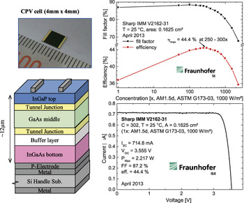
Recently, world-record efficiency (44.4%) has been demonstrated with InGaP/GaAs/InGaAs 3-junction solar cell under 250–300-suns by Sharp Co. under the EU-Japan Collaborative Research on CPV. Figure 3 shows 44.4% efficiency under 250–300-suns with Sharp’s InGaP/GaAs/InGaAs 3-J solar cells Reference Takamoto, Agui, Sasaki and Nakaido9,Reference Yamaguchi, Takamoto, Araki and Kojima10 confirmed by the FhG-ISE.
44.4% efficiency under 250–300-suns with Sharp’s InGaP/GaAs/InGaAs 3-J solar cells confirmed by the FhG-ISE (adapted from Ref. Reference Yamaguchi, Takamoto, Araki and Kojima10 with “Copyright (2016) The Japan Society of Applied Physics”).

C. Research field “creative generation of clean energy using solar energy” under the JST-CREST program
The target of the research field “Creative Clean Energy Generation using Solar Energy” under the JST-CREST program was the R&D for solar cells and materials composing of Si crystals and thin films, compound semiconductors, dye-sensitized and organic materials, and new super high-efficiency solar cells, in addition to the creation of useful materials, such as hydrogen, and the simultaneous creation of useful material and clean energy using solar energy. Reference Yamaguchi11 In this research area, we focused on the basics of material search, fundamental physical analysis (light absorption, charge separation, material deterioration, and so on), and new principles for realizing higher efficiency and longer lifetime, and we will aim for R&D that is creative and becomes one of break-through technologies in the future. For this end, we have combined the expertise of researchers from the different fields of physics, chemistry, and electronic engineering and utilize cutting edge nanotechnology to promote R&D through the fusion of different areas.
Under the JST PV R&D project, the National Institute of Materials Science (NIMS) has achieved high efficiency (11.6%) with dye-sensitized solar cell and 15.0% efficiency with 1 cm2 area perovskite solar cell. Reference Chen, Wu, Yue, Liu, Zhang, Yang, Chen, Bi, Ashraful, Grätzel and Han12
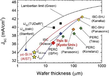
The Kyoto University group has also achieved a high short-circuit current density of 36.1 mA/cm2 with thin 18.5 μm thick thin single-crystalline Si solar cell in addition to 8.64% efficiency (V oc = 562 mV, J sc = 21.6 mA/cm2, FF = 71.4%) with 500 nm thick and 1 cm2 area μc-Si thin-film solar cell by using phonic crystal optical management. Reference Ishizaki, Zoysa, Tanaka, Umeda, Kawamoto and Noda13 Figure 4 shows wafer and thin-film thickness dependence for various Si single-crystalline, multicrystalline and microcrystalline (μc-Si) Si solar cells analyzed by Sai. Reference Sai, Umishio, Matsui, Nunomura, Takato, Kawatsu and Matsubara14 Effectiveness of optical management for more than 20% efficiency by using thin Si wafer of less than 20 μm is shown.
Wafer and thin-film thickness dependence of various single-crystalline, multicrystalline (μc-Si) and microcrystalline Si solar cells (reproduced with permission from Ref. Reference Sai, Umishio, Matsui, Nunomura, Takato, Kawatsu and Matsubara14 [RCPV, AIST], [2017]).

Table II summarizes world-record efficiencies for various solar cells and Japanese contributions. As shown in Table II, Japanese team has contributed to development of high-efficiency solar cells greatly as a result of Japanese national PV R&D programs such as the NEDO projects.
Summary of world-record efficiencies for various solar cells and Japanese contributions.

III. ANALYSIS FOR EFFICIENCY POTENTIAL OF VARIOUS HIGH-EFFICIENCY SOLAR CELLS
This section presents analytical results for high-efficiency potential of single-crystalline Si solar cells, GaAs and III–V compound 3- and 5-junction cells, CIGSe, and CdTe solar cells.
A. Analytical procedure for estimating efficiency potential of high-efficiency solar cells
Radiative recombination lifetime τrad is expressed by
 $${\tau _{{\rm{rad}}}} = {1 \mathord{\left/ {\vphantom {1 {BN}}} \right. \kern-\nulldelimiterspace} {BN}}\quad ,$$
where N is carrier concentration and B is radiative recombination probability. For Si and GaAs, B values are 2 × 10⁻¹⁵ cm3/s and 2 × 10⁻¹⁰ cm3/s, Reference Ahrenkiel, Ahrenkiel and Lundstrom15 respectively. Therefore, optimization of carrier concentration in solar cell layers is necessary by considering minority-carrier lifetime and series resistance. In addition, photon recycling is also important to reduce the impact of radiative recombination and to give lower effective B. Effective lifetime τeff is expressed by
 $${1 \mathord{\left/ {\vphantom {1 {{\tau _{{\rm{eff}}}}}}} \right. \kern-\nulldelimiterspace} {{\tau _{{\rm{eff}}}}}} = {1 \mathord{\left/ {\vphantom {1 {{\tau _{{\rm{rad}}}} + {1 \mathord{\left/ {\vphantom {1 {{\tau _{{\rm{nonrad}}}}}}} \right. \kern-\nulldelimiterspace} {{\tau _{{\rm{nonrad}}}}}}}}} \right. \kern-\nulldelimiterspace} {{\tau _{{\rm{rad}}}} + {1 \mathord{\left/ {\vphantom {1 {{\tau _{{\rm{nonrad}}}}}}} \right. \kern-\nulldelimiterspace} {{\tau _{{\rm{nonrad}}}}}}}}\quad ,$$
where τnonrad is nonradiative recombination lifetime and given by
 $${1 \mathord{\left/ {\vphantom {1 {{\tau _{{\rm{nonrod}}}} = \sigma v{N_{\rm{r}}}}}} \right. \kern-\nulldelimiterspace} {{\tau _{{\rm{nonrod}}}} = \sigma v{N_{\rm{r}}}}}\quad ,$$
where σ is capture cross section of minority-carriers by nonradiative recombination centers, v is minority-carrier thermal velocity, and N r is density of nonradiative recombination center. Therefore, improvement in crystalline quality and reduction in densities of defects such as point defects, dislocations, grain boundaries, interface states, and impurities that act as nonradiative recombination centers are very important.
To realize higher efficiency of various solar cells, improvements in short-circuit density J sc, open-circuit voltage V oc, and fill factor FF are substantially necessary.
The open-circuit voltage V oc is given by
 $${V_{{\rm{oc}}}} = {{kT} \over q}\ln \left( {{{{J_{\rm{L}}}} \over {{J_0}}} + 1} \right)\quad ,$$
where k is Boltzmann constant, T is absolute temperature, q is electronic charge, J L is photon generated current density, and J 0 is saturation current density. To increase V oc, decrease in saturation current density J 0 is essential.
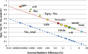
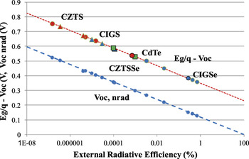
One of problems to attain the higher efficiency solar cells is the higher minority-carrier lifetime in various materials. Figure 5 shows open-circuit voltage drop compared to band gap energy (E g/q − V oc) and nonradiative voltage loss (V oc,nrad) in various solar cells as a function of external radiative efficiency (ERE). Open-circuit voltage is expressed by Reference Rau16–Reference Yao, Kirchartz, Vezie, Faist, Gong, He, Wu, Troughion, Watson, Bryant and Nelson18
 $${V_{{\rm{oc}}}} = {V_{{\rm{oc,rad}}}} + {{kT} \over q}\ln \left( {{\rm{ERE}}} \right)\quad ,$$
where the second term shows nonradiative voltage loss, and V oc,rad is radiative open-circuit voltage and is given by Reference Rau16–Reference Yao, Kirchartz, Vezie, Faist, Gong, He, Wu, Troughion, Watson, Bryant and Nelson18
 $${V_{{\rm{oc,rad}}}} = {{kT} \over q}\ln \left( {{{{J_{\rm{L}}}\left( {{V_{{\rm{oc,rad}}}}} \right)} \over {{J_{0,{\rm{rad}}}}}} + 1} \right)\quad ,$$
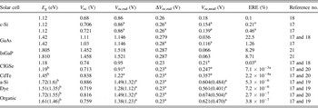
where J L(V oc,rad) is photocurrent at open-circuit in the case of only radiative recombination and J 0,rad is saturation current density in the case of only radiative recombination and 0.28 V was used as the ΔV oc,rad = E g/q − V oc,rad value Reference Yao, Kirchartz, Vezie, Faist, Gong, He, Wu, Troughion, Watson, Bryant and Nelson18 in Fig. 5. Table III shows ERE, voltage losses, and other parameters for various materials and solar cells. Reference Green17–Reference Geisz, Steiner, Garcia, Kurtz and Friedman21 Voltages losses and other parameters were estimated from Eq. (5) by assuming 0.26 V for Si, 0.28 V for GaAs, and 0.23 V for other materials as ΔV oc,rad = E g/q − V oc,rad. Band gap energy E g was estimated from the external quantum efficiency spectrum. Reference Green, Emery, Hishikawa and Warta19,Reference Green, Emery, Hishikawa and Warta20 In the case of a-Si, dye and organic solar cells, there are additional losses Reference Yao, Kirchartz, Vezie, Faist, Gong, He, Wu, Troughion, Watson, Bryant and Nelson18 due to presence of band tails of localized sates as shown for V oc,nrad values in Table III.
Open-circuit voltage drop compared to band gap energy (E g/q − V oc) and nonradiative V oc (V oc,nrad) in various solar cells as a function of ERE.

ERE, voltage losses, and other parameters for various materials and solar cells.

a Voltages losses and other parameters estimated from Eq. (5) by assuming 0.26 V for Si, 0.28 V for GaAs, and 0.23 V for other materials as ΔV oc,rad = E g/q − V oc,rad.
b E g estimated from the external quantum efficiency (EQE) spectrum. (E g) value was estimated by considering band tail in the EQE spectrum.
As shown in Fig. 5, even crystalline Si solar cells have still nonradiative recombination loss and further improvements in efficiency are thought to be possible by improving minority-carrier lifetime and reducing recombination losses.
Fill factor is dependent on V oc and ideal fill factor FF0 used in the calculation is empirically expressed by Reference Green22
 $${\rm{F}}{{\rm{F}}_0} = {{{\nu _{{\rm{oc}}}} - \ln \left( {{\nu _{{\rm{oc}}}} + 0.72} \right)} \over {{\nu _{{\rm{oc}}}} + 1}}\quad ,$$
where νoc is normalized open-circuit voltage and is given by
 $${\nu _{{\rm{oc}}}} = {{{V_{{\rm{oc}}}}} \mathord{\left/ {\vphantom {{{V_{{\rm{oc}}}}} {\left( {{{nkT} \mathord{\left/ {\vphantom {{nkT} q}} \right. \kern-\nulldelimiterspace} q}} \right)}}} \right. \kern-\nulldelimiterspace} {\left( {{{nkT} \mathord{\left/ {\vphantom {{nkT} q}} \right. \kern-\nulldelimiterspace} q}} \right)}}\quad .$$
The fill factor is decreased as increase in series resistance R S and decrease in shunt resistance R Sh of solar cell and approximated by
 $${\rm{FF}} \approx {\rm{F}}{{\rm{F}}_0}\left( {1 - {r_{\rm{s}}}} \right)\left( {1 - {1 \mathord{\left/ {\vphantom {1 {{r_{{\rm{sh}}}}}}} \right. \kern-\nulldelimiterspace} {{r_{{\rm{sh}}}}}}} \right) \approx {\rm{F}}{{\rm{F}}_0}\left( {1 - {r_{\rm{s}}} - {1 \mathord{\left/ {\vphantom {1 {{r_{{\rm{sh}}}}}}} \right. \kern-\nulldelimiterspace} {{r_{{\rm{sh}}}}}}} \right)\quad ,$$
where r s is normalized series resistance and normalized shunt resistance is r sh and given by
 $${r_{\rm{s}}} = {{{R_{\rm{S}}}} \mathord{\left/ {\vphantom {{{R_{\rm{S}}}} {{R_{{\rm{CH}}}}}}} \right. \kern-\nulldelimiterspace} {{R_{{\rm{CH}}}}}}\quad ,$$
 $${r_{{\rm{sh}}}} = {{{R_{{\rm{Sh}}}}} \mathord{\left/ {\vphantom {{{R_{{\rm{Sh}}}}} {{R_{{\rm{CH}}}}}}} \right. \kern-\nulldelimiterspace} {{R_{{\rm{CH}}}}}}\quad .$$
The characteristic resistance R CH is expressed by Reference Green22
 $${R_{{\rm{CH}}}} = {{{V_{{\rm{oc}}}}} \over {{I_{{\rm{sc}}}}}}\quad ,$$
where Isc is short-circuit current.
In the calculation, highest values obtained were used as J sc. V oc and FF were calculated by Eqs. (5)–(9) and conversion efficiency potential of various solar cells were calculated as a function of ERE.
B. Analytical results for efficiency potential of high-efficiency solar cells
1. Efficiency potential of crystalline Si solar cells
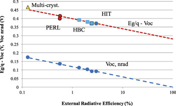
Figure 6 shows open-circuit voltage drop compared to band gap energy (E g/q − V oc) and nonradiative voltage loss (V oc,nrad) in Si solar cells as a function of ERE. In Si, 0.26 V was used as the ΔV oc,rad value. Reference Yao, Kirchartz, Vezie, Faist, Gong, He, Wu, Troughion, Watson, Bryant and Nelson18
Open-circuit voltage drop compared to band gap energy (E g/q − V oc) and nonradiative V oc (V oc,nrad) in Si solar cells as a function of ERE.

In the figure, V oc values for heterojunction with intrinsic thin-layer (HIT) cell, Reference Taguchi, Yano, Tohoda, Matsuyama, Nakamura, Nishiwaki, Fujita and Maruyama23 HBC cells Reference Masuko, Shigematsu, Hashiguchi, Fujishima, Kai, Yoshimura, Yamaguchi, Ichihashi, Yamanishi, Takahama, Taguchi, Maruyama and Okamoto4,Reference Yoshikawa, Kawasaki, Yoshida, Irie, Konishi, Nakano, Uto, Adachi, Kanemitsu, Uzu and Yamamoto5 passivated emitter and rear locally diffused (PERL) cell Reference Green17,Reference Green, Emery, Hishikawa and Warta19,Reference Zhao, Wang, Green and Ferrazza24 and multicrystalline Si cell Reference Green, Emery, Hishikawa, Warta and Dunlop25 and ERE values estimated by using Eq. (5) are plotted except for PERL cell. Reference Green17 The HIT cells have better ERE compared to HBC and PERL cells. Multicrystalline cells have lower ERE values due to lower minority-carrier lifetime. As shown in Fig. 6, crystalline Si solar cells have still nonradiative recombination loss and further improvements in efficiency are thought to be possible by improving minority-carrier lifetime and reducing recombination losses.
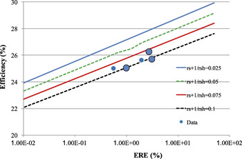
Figure 7 shows calculated efficiency of crystalline Si solar cells as a function of ERE and efficiency values for PERL cell Reference Green17 and HBC cell Reference Masuko, Shigematsu, Hashiguchi, Fujishima, Kai, Yoshimura, Yamaguchi, Ichihashi, Yamanishi, Takahama, Taguchi, Maruyama and Okamoto4,Reference Yoshikawa, Kawasaki, Yoshida, Irie, Konishi, Nakano, Uto, Adachi, Kanemitsu, Uzu and Yamamoto5 as a function of ERE. In the figure, ERE values estimated by using Eq. (5) are plotted except for PERL cell. Reference Green17 Although the PERL cell shows the highest J sc, improvement in V oc is a problem to be solved. On the other hand, regarding the HBC cell shows the higher V oc, improvement in J sc is a problem to be solved. As shown in Fig. 7, crystalline Si solar cells have still nonradiative loss and further improvements in efficiency are thought to be possible by improving minority-carrier lifetime and reducing recombination losses as a results of increasing ERE and decreasing r s + 1/r sh.
Calculated efficiency of crystalline Si solar cells as a function of ERE and r s + 1/r sh in comparison with efficiencies of PERL and HBC cells.

On the other hand, regarding the HIT cell shows the highest V oc, improvement in J sc is a problem to be solved, improvements in V oc are necessary. The HBC cells have potential of higher V oc and J sc. In summary, efficiencies over 28% such as 28.0, 28.5, and 28.8% will be realized with r s + 1/r sh of 0.05 by improvements in ERE into 10%, 20%, and 30%, respectively, from around 1% as shown in Fig. 7.
2. Efficiency potential of GaAs and GaAs-on-Si solar cells
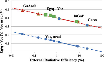
Figure 8 shows open-circuit voltage drop compared to band gap energy (E g/q − V oc) and nonradiative voltage loss (V oc,nrad) in GaAs, InGaP, and GaAs/Si solar cells Reference Green17,Reference Yao, Kirchartz, Vezie, Faist, Gong, He, Wu, Troughion, Watson, Bryant and Nelson18,Reference Geisz, Steiner, Garcia, Kurtz and Friedman21,Reference Green, Emery, Hishikawa, Warta and Dunlop25–Reference Yamaguchi, Ohmachi, Oh’hara, Kadota, Imaizumi and Matsuda29 as a function of ERE. In the figure, ERE values estimated by using Eq. (5) are plotted except for GaAs cells reported by Alta Devices Reference Green17,Reference Yao, Kirchartz, Vezie, Faist, Gong, He, Wu, Troughion, Watson, Bryant and Nelson18,Reference Green, Emery, Hishikawa, Warta and Dunlop25,Reference Kayes, Nie, Twist, Sproytee, Reinhardt, Kizilyalli and Higashi26 and FhG-ISE Reference Green17,Reference Green, Emery, Hishikawa, Warta and Dunlop25 and InGaP cell reported by NREL. Reference Geisz, Steiner, Garcia, Kurtz and Friedman21 0.28 V for GaAs and GaAs/Si, and 0.287 V for InGaP was used as the ΔV oc,rad values Reference Yao, Kirchartz, Vezie, Faist, Gong, He, Wu, Troughion, Watson, Bryant and Nelson18,Reference Geisz, Steiner, Garcia, Kurtz and Friedman21 in this study.
Open-circuit voltage drop compared to band gap energy (E g/q − V oc) and nonradiative V oc (V oc,nrad) in GaAs, InGaP, and GaAs/Si solar cells as a function of ERE.

As shown in Fig. 8, higher ERE values of 22.5 Reference Green17 and 8.71% Reference Geisz, Steiner, Garcia, Kurtz and Friedman21 for GaAs and InGaP, respectively, compared to those of crystalline SI, CIGSe, and CdTe have been obtained as a results of high-quality thin-layer, reducing front and rear surface and interface recombination, and optical management. Reference Kayes, Nie, Twist, Sproytee, Reinhardt, Kizilyalli and Higashi26 On the other hand, GaAs/Si and III–V/Si tandem solar cells Reference Yamaguchi, Lee, Araki, Kojima and Ohshita27–Reference Yamaguchi, Ohmachi, Oh’hara, Kadota, Imaizumi and Matsuda29 have larger voltage drop due to lower ERE values of about 0.1%. Therefore, reduction in dislocation density for GaAs/Si from 106 cm−2 to less than 105 cm−2 is necessary. Reference Yamaguchi and Amano30
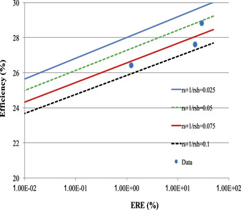
Figure 9 shows calculated efficiency of GaAs solar cells as a function of ERE and efficiency values for GaAs solar cells by Alta Devices Reference Green17,Reference Green, Emery, Hishikawa, Warta and Dunlop25,Reference Kayes, Nie, Twist, Sproytee, Reinhardt, Kizilyalli and Higashi26 and FhG-ISE. Reference Green17,Reference Green, Emery, Hishikawa and Warta19,Reference Green, Emery, Hishikawa and Warta20 Although the GaAs solar cells have realized highest ERE of 22.5%, Reference Green17 further improvement in efficiency is also thought to be possible by improving minority-carrier lifetime and reducing recombination losses as a results of increasing ERE and decreasing r s + 1/r sh. In summary, efficiencies over 29% such as 29.7 and 30.0% will be realized with r s + 1/r sh of 0.025 by improvements in ERE into 30 and 40%, respectively from 22.5% as shown in Fig. 9.
Calculated efficiency of GaAs solar cells as a function of ERE and r s + 1/r sh in comparison with efficiencies of GaAs solar cells reported by Alta Devices and FhG-ISE.

In the case of GaAs/Si solar cells, reduction in dislocation density in GaAs/Si is necessary for realizing high-efficiency solar cells. The effective minority-carrier lifetime τeff is expressed by the following equation Reference Yamaguchi and Amano30 :
 $${1 \mathord{\left/ {\vphantom {1 {{\tau _{{\rm{eff}}}}}}} \right. \kern-\nulldelimiterspace} {{\tau _{{\rm{eff}}}}}} = {1 \mathord{\left/ {\vphantom {1 {{\tau _{{\rm{rad}}}}}}} \right. \kern-\nulldelimiterspace} {{\tau _{{\rm{rad}}}}}} + {1 \mathord{\left/ {\vphantom {1 {{\tau _{\rm{d}}}}}} \right. \kern-\nulldelimiterspace} {{\tau _{\rm{d}}}}} = BN + {\pi ^3}{{{N_{\rm{d}}}D} \mathord{\left/ {\vphantom {{{N_{\rm{d}}}D} 4}} \right. \kern-\nulldelimiterspace} 4}\quad ,$$
where τrad is minority-carrier lifetime for radiative recombination, B is the radiative recombination probability, and N is the carrier concentration. For GaAs, B value is 2 × 10⁻¹⁰ cm3/s. Reference Ahrenkiel, Ahrenkiel and Lundstrom15
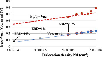
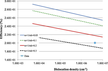
Figure 10 shows open-circuit voltage drop compared to band gap energy (E g/q − V oc) and nonradiative V oc (V oc,nrad) in GaAs/Si solar cells Reference Ringell, Carlinl, Andre, Hudait, Gonzalez, Wilt, Clark, Jenkins, Scheiman, Allerman, Fitzgerald and Leitz28,Reference Yamaguchi, Ohmachi, Oh’hara, Kadota, Imaizumi and Matsuda29 as a function of dislocation density and ERE. In this figure, nonradiative voltage loss as expressed by the following equation was estimated by using Eq. (13).
 $${V_{{\rm{oc,nrad}}}} = {{kT} \over q}\ln \left[ {{{{\tau _{{\rm{nonrad}}}}} \mathord{\left/ {\vphantom {{{\tau _{{\rm{nonrad}}}}} {\left( {{\tau _{{\rm{rad}}}} + {\tau _{{\rm{nonrad}}}}} \right)}}} \right. \kern-\nulldelimiterspace} {\left( {{\tau _{{\rm{rad}}}} + {\tau _{{\rm{nonrad}}}}} \right)}}} \right]$$
Open-circuit voltage drop compared to band gap energy (E g/q − V oc) and nonradiative V oc (V oc,nrad) in GaAs/Si solar cell as a function of dislocation density and ERE.

To realize higher efficiency III–V/Si tandem solar cells, increasing ERE of more than 1% in III–V/Si due to deceasing dislocation density of less than 105 cm−2 in III–V/Si is necessary as shown in Fig. 10.
Figure 11 shows calculated efficiency of GaAs/Si solar cells as a function of ERE and r s + r sh in comparison with efficiencies of GaAs/Si cells reported by NTT. Reference Yamaguchi, Ohmachi, Oh’hara, Kadota, Imaizumi and Matsuda29 In summary, efficiencies over 27% such as 27.4 and 28.4% will be realized with r s + 1/r sh of 0.05 by improvements in ERE into 1% and 10%, respectively from 0.1% as a result of reduction on dislocation density in GaAs/Si from 106 cm−2 to 105 cm−2 and 104 cm−2, respectively, as shown in Fig. 11.
Calculated efficiency of GaAs/Si solar cells as a function of ERE and r s + 1/r sh in comparison with efficiencies of GaAs/Si cells reported by NTT.

3. Efficiency potential of III–V compound multijunction solar cells
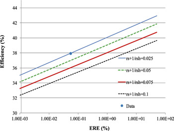
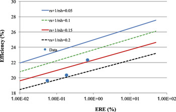
Figure 12 shows calculated efficiency of III–V compound 3-junction solar cells as a function of ERE and efficiency value for 3-junction solar cells by Sharp Reference Sasaki, Agui, Naaido, Takahasi, Onitsuka and Takamoto31 as a function of ERE. Although the 3-junction solar cells have realized a high efficiency of 37.9% under 1-sun condition, Reference Yamaguchi and Amano30 further improvement in efficiency are also thought to be possible by improving minority-carrier lifetime and reducing recombination losses as a results of increasing ERE. In summary, 1-sun efficiencies over 40% such as 40 and 42% will be realized with r s + 1/r sh of 0.025 by improvements in ERE into 1% and 10%, respectively, from 0.06% as shown in Fig. 12.
Calculated 1-sun efficiency of III–V 3-junction solar cells as a function of ERE and r s + 1/r sh in comparison with efficiencies of 3-junction solar cells reported by Sharp.

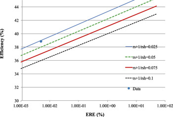
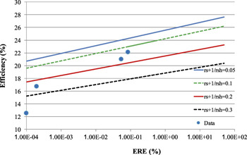
Figure 13 shows calculated 1-sun efficiency of III–V 5-junction solar cells as a function of ERE and efficiency value for 3-junction solar cells by Spectrolab Reference Chiu, Law, Woo, Singer, Bhusan, Hong, Zakaria, Boisvert, Mestropian, King and Karam32 as a function of ERE. Although the 5-junction solar cells have realized high efficiency of 38.8% under 1-sun condition, Reference Sasaki, Agui, Naaido, Takahasi, Onitsuka and Takamoto31 further improvement in efficiency are also thought to be possible by improving minority-carrier lifetime and reducing recombination losses as a results of increasing ERE. In summary, 1-sun efficiencies over 40% such as 42, 43, and 45% will be realized with r s + 1/r sh of 0.025 by improvements in ERE into 0.1%, 1%, and 10%, respectively from 0.005% as shown in Fig. 13.
Calculated 1-sun efficiency of III–V 5-junction solar cells as a function of ERE and r s + 1/r sh in comparison with efficiencies of 5-junction solar cells reported by Spectrolab.

4. Efficiency potential of CuInGaSe2 and CdTe solar cells
Figure 14 shows open-circuit voltage drop compared to band gap energy (E g/q − V oc) and nonradiative voltage loss (V oc,nrad) in CIGSe (CuInGaSe2), CIGS (CuInGaS2), CdTe, CZTSSe (Cu2ZnSn(S,Se)4), and CZTS (Cu2ZnSnS4) solar cells Reference Green17–Reference Green, Emery, Hishikawa and Warta20,Reference Green, Emery, Hishikawa, Warta and Dunlop25,Reference Kamada, Yagioka, Adachi, Handa, Tai, Kato and Sugimoto33–Reference Hiroi, Sakai, Kato and Sugimoto35 as a function of ERE. In the figure, ERE values estimated by using Eq. (5) are plotted except for CIGSe cells reported by ZSW and NREL Reference Green17–Reference Green, Emery, Hishikawa and Warta20,Reference Green, Emery, Hishikawa, Warta and Dunlop25 and CdTe cell reported by ASP. Reference Green17–Reference Green, Emery, Hishikawa and Warta20,Reference Green, Emery, Hishikawa, Warta and Dunlop25 In CIGaSe, 0.23 V was used as the ΔV oc,rad value Reference Yao, Kirchartz, Vezie, Faist, Gong, He, Wu, Troughion, Watson, Bryant and Nelson18 in this study. As shown in Fig. 14, CIGSe and CdTe solar cells have still nonradiative recombination loss and further improvements in efficiency are thought to be possible by improving minority-carrier lifetime and reducing recombination losses. In addition, CIGS, CZTS, and CZTSSe solar cells have much larger nonradiative recombination loss compared to that in CIGSSe and CdTe cells.
Open-circuit voltage drop compared to band gap energy (E g/q − V oc) and nonradiative V oc (V oc,nrad) in CIGSe, CIGS, CdTe, CZTSSe and CZTS solar cells as a function of ERE.

Figure 15 shows calculated efficiency of CIGaSe solar cells as a function of ERE Reference Green17 and efficiency values for CIGaSe cells reported by Solar Frontier, Reference Kamada, Yagioka, Adachi, Handa, Tai, Kato and Sugimoto33,Reference Hiroi, Sakai, Kato and Sugimoto35 ZSW, Reference Green17,Reference Green, Emery, Hishikawa and Warta19,Reference Green, Emery, Hishikawa and Warta20 and NREL. Reference Green17,Reference Green, Emery, Hishikawa and Warta19,Reference Green, Emery, Hishikawa and Warta20
Calculated efficiency of CIGSe solar cells as a function of ERE and r s + r sh in comparison with efficiencies of CIGSe solar cells reported by Solar Frontier, ZSW and NREL.

In summary, in the CIGaSe solar cells, efficiencies over 26% such as 26.0 and 26.5% will be realized with r s + r sh of 0.05 by improvements in ERE into 5%, and 10%, respectively, from around 0.5% as shown in Fig. 15.
Figure 16 shows calculated efficiency of CdTe solar cells as a function of ERE Reference Rau16 and efficiency values for CdTe cells reported by ASP Reference Green17,Reference Green, Emery, Hishikawa and Warta19,Reference Green, Emery, Hishikawa and Warta20 and First Solar. Reference Green, Emery, Hishikawa and Warta19,Reference Green, Emery, Hishikawa and Warta20,Reference Green, Emery, Hishikawa, Warta, Dunlop, Levi and Ho-Baillie36
Calculated efficiency of CdTe solar cells as a function of ERE and r s + r sh in comparison with efficiencies of CdTe solar cells reported by ASP and First Solar.

In summary, in the CdTe solar cells, efficiencies over 26% such as 25.9 and 26.4% will be realized with r s + r sh of 0.05 by improvements in ERE into 2% and 5%, respectively, from around 0.1% as shown in Fig. 16.
The efficiency potential for future generation solar cells such as perovskite, dye-sensitized, organic, multiquantum well, quantum dot, Cu2ZnSnS(Se)4, and ferro-electric solar cells will be discussed elsewhere. Reference Yamaguch, Lee, Araki, Kojima, Yamada and Katsumata37
IV. DISCUSSION ABOUT KEY ISSUES FOR FURTHER EFFICIENCY IMPROVEMENT OF SOLAR CELLS
Further improvements in minority-carrier lifetime based on understanding defect behavior in addition to improvements in front-surface, rear-surface, and interface passivation and decease in series resistance and shunt resistance is thought to be very important to realize higher efficiency solar cells.
According to efficiency simulation for the crystalline Si solar cells by Swanson, Reference Swanson38 in the case of effective lifetime of 10 and 100 ms, efficiency potential of Si solar cells have shown an efficiency of 27.3% and 28%, respectively. It is suggested that the cell efficiency using practical and available silicon material is over 27%, providing that contacts with sufficiently low recombination can be realized. Reference Swanson38
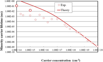
Figure 17 shows changes in minority-carrier lifetime in Si Reference Dziewior and Schmid39,Reference Higasa, Nagai, Nakagawa and Kashima40 as a function of carrier concentration. In the figure, calculated values of minority-carrier lifetime were also shown by using the following equation:
 $${1 \mathord{\left/ {\vphantom {1 \tau }} \right. \kern-\nulldelimiterspace} \tau } = BN + C{N^2}\quad ,$$
where B is radiative recombination probability and 2 × 10⁻¹⁵ cm3/s Reference Ahrenkiel, Ahrenkiel and Lundstrom15 for Si, N is carrier concentration, and C is the Auger coefficient and is 1.6 × 10⁻³⁰ cm6/s Reference Dziewior and Schmid39 for Si. As shown in Fig. 17, further improvement in minority-carrier lifetime is expected to be realized, especially in low carrier concentration range of less than 1016 cm−3. Really, high bulk lifetime of around 100 ms has been obtained by the magnetic field-applied Czochralski method and decreasing carbon concentration to less than 1014 cm−3 in Si. Reference Higasa, Nagai, Nakagawa and Kashima40 Therefore, improvement in Si crystalline quality and reduction in densities of defects such as dislocations, grain boundaries, and impurities that act as nonradiative recombination centers.
Changes in minority-carrier lifetime in Si as a function of carrier concentration (reproduced with permission from Ref. Reference Dziewior and Schmid39 [AIP], [1999]).

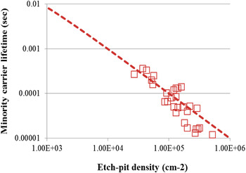
In the case of multicrystalline solar cells, one of major problems for realizing higher efficiency is higher dislocation density. Figure 18 shows our results for changes in minority-carrier lifetime in multicrystalline Si as a function of etch-pit (dislocation) density. Reference Arafune, Sasaki, Wakabayashi, Terada, Ohshita and Yamaguchi41 Dislocation density N d dependence of effective lifetime τeff is given by
 $${1 \mathord{\left/ {\vphantom {1 {{\tau _{{\rm{eff}}}}}}} \right. \kern-\nulldelimiterspace} {{\tau _{{\rm{eff}}}}}}\left[ {{{\mathop{\rm s}\nolimits} ^{ - 1}}} \right] = BN + 0.1 \times {N_{\rm{d}}}\left[ {{\rm{c}}{{\rm{m}}^{ - 2}}} \right]\quad .$$
Changes in minority-carrier lifetime in multicrystalline Si as a function of etch-pit density (reproduced with permission from Ref. Reference Arafune, Sasaki, Wakabayashi, Terada, Ohshita and Yamaguchi41 [Elsevier], [2006]).

As already discussed above, the open-circuit voltage drop compared to band gap energy (E g/q − V oc) and nonradiative V oc (V oc,nrad) can be estimated from Eqs. (5), (14), and (16) in multicrystalline Si solar cells as a function of dislocation density in Si. The lower dislocation density of less than 3 × 103 cm−2 will provide a lower voltage drop of less than 0.4 V and higher V oc of more than 700 mV. Decreasing dislocation density is suggested for realizing higher bulk lifetime and for higher efficiency multicrystalline Si solar cells of more than 24%.
Because the effective lifetime is expressed by the following equation, front-surface, rear-surface, and interface passivation is very effective for realizing higher efficiency.
 $${1 \mathord{\left/ {\vphantom {1 {{\tau _{{\rm{eff}}}}}}} \right. \kern-\nulldelimiterspace} {{\tau _{{\rm{eff}}}}}} = BN + {1 \mathord{\left/ {\vphantom {1 {{\tau _{{\rm{nonrad}}}}}}} \right. \kern-\nulldelimiterspace} {{\tau _{{\rm{nonrad}}}}}} + {{2S} \mathord{\left/ {\vphantom {{2S} d}} \right. \kern-\nulldelimiterspace} d}\quad ,$$
where S is surface recombination velocity and d is layer thickness.
In the III–V compound material solar cells, because GaAs has large surface recombination velocity S of around 1 × 107 cm/s, Reference Casey and Beehler42 shallow homojunction with a junction depth of less than 50 nm is necessary to obtain high-efficiency. Therefore, double-hetero structure solar cells are widely used for high-efficiency solar cells. On the other hand, InP has better surface property with surface recombination velocity S of around 1 × 103 cm/s. Reference Casey and Beehler42 Regarding the differences of surface recombination velocities in semiconductor materials, differences of point defect behavior are thought to be one of the mechanisms. For example, because nearest-neighbor hopping migration energies (0.3 and 1.2 eV) of V In and V P in InP Reference Van Vechten and Wagner43 are lower than those (1.75 eV) of V Ga and V As in GaAs, better surface state may be formed on InP surface compared to GaAs surface. Reference Van Vechten and Wagner43–Reference Yamaguchi and Ando45
In the case of crystalline Si solar cells, device structures have also been improved from conventional n-on-p homojunction solar cells, back surface field cells, passivated emitter and rear locally diffused (PERL, front emitter surface is passivated with oxide, boron locally diffused for rear contact and rear surface is also passivated with oxide) Reference Zhao, Wang, Green and Ferrazza24 or passivated emitter and rear (front emitter surface is passivated with oxide, un- diffused rear contact and rear surface is also passivated with oxide) cell type cells, Reference Blakers, Wang, Milne, Zhao and Green46 back-contact cells, Reference Swanson, Beckwith, Crane, Eaides, Kwark, Sinon and Swiiwiun47 heterojunction cells Reference Taguchi, Yano, Tohoda, Matsuyama, Nakamura, Nishiwaki, Fujita and Maruyama23 to back-contact heterojunction solar cells. Reference Masuko, Shigematsu, Hashiguchi, Fujishima, Kai, Yoshimura, Yamaguchi, Ichihashi, Yamanishi, Takahama, Taguchi, Maruyama and Okamoto4
Lattice mismatching also degrades solar cell properties by increase in interface recombination velocity as a result of misfit dislocations and threading dislocations generation. Lattice mismatch (Δa/a 0) dependence of interface recombination velocity (S I) is semiempirically expressed by Reference Neuse48,Reference Yamaguchi49
 $${S_{\rm{I}}}\left[ {{\rm{cm/s}}} \right] = 1.5 \times {10^8}{{\Delta a} \mathord{\left/ {\vphantom {{\Delta a} {{a_0}}}} \right. \kern-\nulldelimiterspace} {{a_0}}}\quad .$$
Therefore, lattice constant matching between active layers, buffer layers, and substrates is necessary to realize higher efficiency.
Photon recycling is thought to be very effective for improving V oc, J sc, and efficiency of solar cells. The highest 1-sun efficiency (Eff. = 28.8%, V oc = 1.122 V, J sc = 29.68 mA/cm2, FF = 86.5%) GaAs thin-film (2.5 μm thick) single-junction solar cells have been demonstrated by the Alta Devices. Reference Kayes, Nie, Twist, Sproytee, Reinhardt, Kizilyalli and Higashi26 About 0.1 V higher V oc compared to conventional GaAs solar cells has been attained as a result of photon recycling effect. Higher efficiency of more than 30% with GaAs thin-film solar cells is also expected to be realized by using strong internal and ERE. Reference Miller, Yablonovitch and Kurtz50
V. SUMMARY
The present status of R&D for various types of solar cells is presented by overviewing research and development projects for solar cells in Japan as the Project Leader of the previous PV R&D Project “High Performance Photovoltaic System Technology Development for the Future” under NEDO of Japan and as the Research Supervisor of the Research Filed “Creative Clean Energy Generation by using Solar Energy” under the JST. Developments of high-efficiency solar cells such as 44.4% (under concentration) and 37.9% (under 1-sun) InGaP/GaAs/InGaAs 3-junction solar cells by Sharp, 25.1% crystalline Si HBC solar cells by Sharp, 20.9% CIGS solar cells by Solar Frontier, and 11.9% dye-sensitized solar cells by Sharp have been demonstrated under the previous NEDO PV R&D Project. 15.0% efficiency has also been attained with 1 cm2 perovskite solar cell by NIMS under the JST Project. Most recently, 26.6% crystalline Si HBC solar cells by Kaneka, 22.3% CIGS solar cells by Solar Frontier, and 18.2% perovskite solar cell by NIMS have been achieved under the present NEDO PV R&D Project.
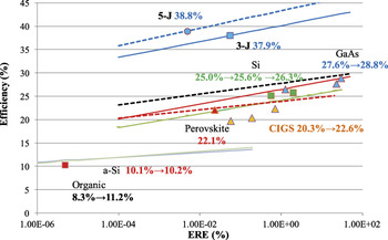
Efficiency potential of high-efficiency solar cells such as crystalline Si, GaAs, GaAs/Si, III–V multijunction, CIGSe, and CdTe solar cells is discussed based on ERE, open-circuit voltage loss and fill factor loss. Figure 19 summarizes efficiency potential of various solar cells analyzed in this study.
Summary of efficiency potential of various solar cells analyzed in this study.

In summary,
-
(1) Crystalline Si solar cells have potential efficiencies over 28% such as 28.0, 28.5, and 28.8% with normalized series resistance and shunt resistance r s + 1/r sh of 0.05 by improvements in ERE into 10%, 20%, and 30%, respectively, from around 1%.
-
(2) GaAs solar cells have potential efficiencies over 29% such as 29.7 and 30.0% with r s + 1/r sh of 0.025 by improvements in ERE into 30% and 40%, respectively from 22.5%.
GaAs/Si solar cells have potential efficiencies over 27% such as 27.4 and 28.4% with r s + r sh of 0.05 by improvements in ERE into 1% and 10%, respectively from 0.1% as a result of reduction on dislocation density in GaAs/Si from 106 cm−2 to 105 cm−2 and 104 cm−2, respectively.
-
(3) III–V compound 3-junction solar cells have 1-sun potential efficiencies over 40% such as 40 and 42% with r s + 1/r sh of 0.025 by improvements in ERE into 1% and 10%, respectively from 0.06%. 5-junction solar cells have 1-sun potential efficiencies over 40% such as 42, 43, and 45% with r s + 1/r sh of 0.025 by improvements in ERE into 0.1%, 1%, and 10%, respectively, from 0.005.
-
(4) CIGSe solar cells have potential efficiencies over 26% such as 26.0, and 26.5% with r s + 1/r sh of 0.05 by improvements in ERE into 5% and 10%, respectively, from around 0.5%.
-
(5) CdTe solar cells have potential efficiencies over 26% such as 25.9 and 26.4% with r s + 1/r sh of 0.05 by improvements in ERE into 2% and 5%, respectively, from around 0.1%.
For this end, further improvements in minority-carrier lifetime based on understanding defect behavior in addition to improvements in front-surface, rear-surface, and interface passivation and decease in series resistance and shunt resistance is suggested to realize higher efficiency solar cells.
Supplementary Material
To view supplementary material for this article, please visit https://doi.org/10.1557/jmr.2017.335.
ACKNOWLEDGMENTS
This work was partially supported by the NEDO under the METI and the JST. The authors thank members in the NEDO, METI and JST, and to Prof. Y. Ohshita, Prof. A. Yamamoto, Dr. Y. Hayashi and Dr. K. Nakamura, Toyota Tech. Inst., Dr. T. Takamoto and Dr. J. Nakamura, Sharp, Dr. M. Tanaka, Dr. M. Taguchi, Dr. S. Yata, Dr. K. Masuko and Mr. T. Hashiguchi, Panasonic, Dr. H. Sugimoto and Mr. H. Hiroi, Solar Frontier, Dr. H. Sai, and Dr. K. Matsubara, AIST for their cooperation and providing fruitful information.