I. INTRODUCTION
Micromachined electromechanical filters have been long desired as a replacement for off-chip components commonly used in wireless transceiver architectures. The unique advantage of these silicon-based components is the potential for integration with the rest of the electronics, which ultimately improves the level of integrity and complexity in next-generation wireless analog signal processing units. This feature is particularly attractive in multi-band transceivers that operate over a wide frequency spectrum and require arrays of filters with large Q values and small shape factors that fit in a compact portable package. Developing a miniaturized micromechanical filter that meets the requirements on insertion loss (IL), selectivity, and power handling all at once is a challenging task that has rarely been accomplished in the past.
Capacitive coupled-resonator filters have proved to be reliable in providing excellent selectivity fueled by minimal acoustic loss [Reference Ayazi, Pourkamali, Ho and Abdolvand1, Reference Sheng-Shian, Demirci, Yu-Wei, Zeying and Nguyen2]. Unfortunately, these devices usually suffer from high IL if terminated to 50 Ω. This problem is more prominent at higher frequencies as a result of less efficient electromechanical coupling. On the other hand, piezoelectric transduction with orders of magnitude larger coupling coefficients offers a superior alternative for enabling low-IL filters. Today, piezoelectric film bulk acoustic resonators (FBARs) have been implemented in front-end transceiver circuits in the GHz frequency range [Reference Ruby, Bradley, Clark, Feld, Jamneala and Wang3]. A number of FBARs are electrically connected in a ladder configuration to provide low-loss high-order filters with a very sharp roll-off skirt. However, for these electrically coupled filters to provide adequate out-of-band rejection, the number of resonators in the coupling chain should be considerably large (between four and ten). Moreover, the center frequency of an FBAR filter is mostly defined by the thickness of the deposited piezoelectric film and therefore devices fabricated on a substrate can only have close (if not the same) center frequencies. Therefore, electrically coupled FBAR filters span a relatively large area, and fail to offer an integrated solution for covering dispersed frequencies over a wide range, which eventually may limit their application.
On the other hand, in an acoustically coupled filter, the capacitive path between input and output ports is significantly smaller compared to a ladder filter of the same order. This is the key to reach large out-of-band rejection in a small, low-order filter. Second-order stacked thin-film piezoelectric BAW filters have been demonstrated with narrow passbands and excellent isolation suitable for applications in which small size is critical or single-ended to differential-ended operation is desired [Reference Lakin4, Reference Small, Jamneala, Callaghan, Larson and Ruby5]. The principle of operation for these acoustically coupled filters is the same as stacked crystal filters [Reference Ballato and Lukaszek6]. However, the fabrication process is relatively complicated in the sense that multiple precisely controlled thin-film deposition steps are involved and thickness inaccuracy can degrade the performance of the filter. These filters also suffer from single-band operation on a chip.
In this work, we introduce an alternative class of acoustically coupled piezoelectric filters called monolithic thin-film piezoelectric-on-substrate (TPoS) filters. Multiple resonance modes of a single resonant structure are coupled in order to achieve a higher order system. The same technique has been implemented in monolithic crystal filter (MCF) technology for decades [Reference Beaver7]. In an MFC, by properly patterning isolated metal electrodes on a single quartz plate, multiple resonance modes of the plate are coupled at low frequencies. Theoretically, different classes of resonance modes such as flexural, rotational, and extensional can be utilized to create monolithic filters. Yet, a great majority of the MCFs have been based on coupled thickness modes [Reference Beaver7, Reference Kinsman8]. The center frequency of these filters is not usually more than a few tens of MHz and is limited to the thinnest crystal plate that can be reproducibly manufactured. As mentioned earlier, with the emergence of thin-film technologies very high frequency (few GHz) thickness mode piezoelectric filters have been demonstrated and commercialized (FBAR filters). However, the technique most attractive for low-frequency crystal filters (mode coupling) has not been adopted for application in this new generation of acoustic devices.
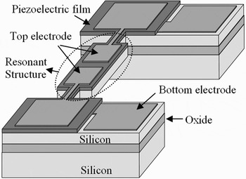
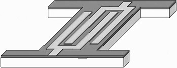
Our attempt in this paper is to demonstrate the potential for the same acoustic coupling technique to be utilized in thin-film piezoelectric devices at high frequencies. A similar dual-mode coupling technique has been demonstrated in thin-film AlN annular structures at low frequencies (~22 MHz) [Reference Stephanou, Piazza, White, Wijesundara and Pisano9]. The resonant structure in our work is a suspended rectangular stack of piezoelectric material (e.g. ZnO) sandwiched between 2 metal electrodes on top of a substrate layer such as silicon (Fig. 1). Silicon substrate with high acoustic velocity and low acoustic loss is used to improve resonance frequency, quality factor, and structural integrity [Reference Ho, Abdolvand, Sivapurapu, Humad and Ayazi10]. High energy density of the silicon substrate can also enhance the linearity of the device [Reference Abdolvand and Ayazi11]. Dispersed-frequency filters can be fabricated on a single substrate by changing the lateral geometry of the filters. We demonstrate a slight frequency shift in thickness mode filters and a broad frequency coverage in lateral mode filters fabricated on a single substrate. The bandwidth (BW) in these filters can also be controlled by changing the device dimensions and electrode pattern. Preliminary guidelines for the design of monolithic thin-film piezoelectric filters are presented in the following.
II. DESIGN PRINCIPLES
A monolithic TPoS filter is structurally the same as a 2-port TPoS resonator [Reference Abdolvand and Ayazi12]. In these devices the input electrical signal applied to one set of electrodes induces a stress field inside the thin piezoelectric film that is sandwiched between the two electrodes. A piezoelectric material with a non-zero d 31 coefficient creates lateral (in-plane) force components that can excite lateral resonant modes of the underlying substrate. The main difference between a TPoS resonator and a filter is in the top electrode pattern. In a TPoS filter, the top electrode is purposely patterned to enable excitation of the dual resonance modes of the released structure. The two modes can be identified as symmetric and anti-symmetric. In symmetric mode the strain field under both electrodes is in phase, whereas in anti-symmetric mode the developed strain field under both electrodes is 180° out of phase. The transfer function of this coupled-mode system is of 4th order (2nd-order filter) [Reference Mason13]. Higher order filters (3rd, 4th, etc.) can also be realized using the same concept, but we will limit our discussion to 2nd-order filters in this work.
MCFs have always attracted attention because of their small size, ease of fabrication, and therefore lower manufacturing cost. Monolithic TPoS filters are also believed to inherit the same advantages over other types of micromachined filters. By coupling multiple modes of a single resonant structure, the need for a discrete coupling element is eliminated, which simplifies the design and fabrication process and reduces the overall area consumption. The issues to be addressed are design procedures for choosing the device shape and patterning the electrodes in order to control the filter BW and to suppress unwanted modes.
Simulating the resonance mode shape of a chosen structure using a finite-element analysis (FEA) software provides considerable insight into the design of the electrode pattern. Depending on the frequency of interest, different categories of resonance modes can be employed for monolithic TPoS filters. For LF to IF frequency band flexural resonance modes are suitable. Lateral extensional resonance modes suit IF to low RF applications and thickness extensional modes are of interest for the GHz range. Once the dual mode shapes are recognized, the surface area of the structure can be split into half and regions with identical strain polarity should be covered with connected pieces of metal electrode on each side. Connecting areas with opposite polarity strain field results in charge cancellation and reduces the coupling coefficient.
In theory, this design method can be practised for all cases. However, the method loses applicability when the resonant structure is a multi-layer composite stack of material and is widened in order to reduce the motional impedance and IL of the filter. Finding resonance mode shapes of such structures requires a very large number of meshing elements in FEA simulators, which makes the method impractical. Nevertheless, some intuitive design rules extracted from simulating simple structures can be loosely applied to more complicated situations. In the following sections, 2 classes of resonance modes in a simple rectangular plate are examined to identify some design rules.
A) Lateral mode
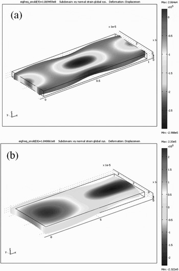
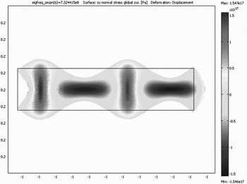
We assume a 40-μm-wide rectangular silicon plate (similar to Fig. 1) as the resonant structure. For the symmetric width-extensional mode, the resonant body undergoes in-phase expansion and contraction along the length of the structure as seen in the mode shape of Fig. 2(a). However, for the anti-symmetric width-extensional mode shape, the displacement in the two halves of the structure (along the length) is out-of-phase (Fig. 2(b)). From these mode shapes it can be concluded that by splitting the top electrode into 2 isolated pieces in the TPoS device, both modes can be excited. The system transfer function from one port to the other is of 4th order (two-pole filter).
Schematic diagram of a monolithic TPoS filter.

Dual fundamental width-extensional mode shapes of a 40-μm-wide silicon plate simulated in COMSOL.

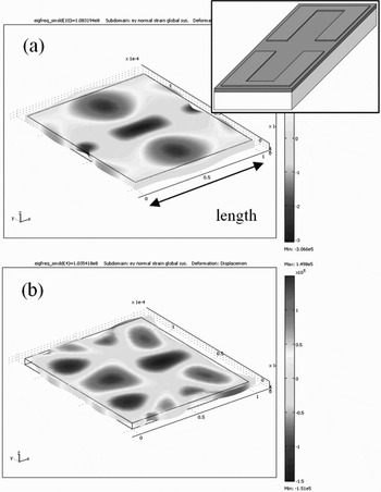
Based on the same discussed concept, dual high-order width-extensional modes of a plate can be excited and coupled. By increasing the mode number (device width), the actuation area can be increased at the same frequency and therefore motional impedance is lowered [Reference Ho, Abdolvand and Ayazi14]. This is critical for implementation of monolithic lateral filters at high frequencies. Dual 3rd-order lateral extensional mode shapes of a 120-μm-wide plate are simulated in Fig. 3. The optimized top electrode pattern for excitation of this mode shape in a TPoS structure is a multi-finger electrode that matches the strain field and is split into half from the middle (inset picture of Fig. 3(a)). The center-to-center finger pitch is equal to the acoustic wavelength in this design. Theoretically, the same pattern can be repeated in order to further reduce the IL.
Dual 3rd-order width-extensional resonance mode shapes of a 120-μm-wide silicon plate and schematic viewgraph of the suggested electrode pattern (inset picture).

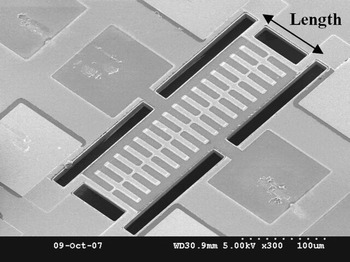
The critical dimension that defines the center frequency in a lateral mode monolithic filter is the width of the plate (or the finger pitch). On the other hand, the length of the device has an interesting effect that can be employed to design the BW of the filter. It is observed in simulations that changing the length (marked in Fig. 3(a)) of the plate will affect the frequency spacing between dual modes. Therefore, the BW of a filter at a certain center frequency can be modified by changing the length of the plate (the BW will increase by decreasing the length). This trend is experimentally verified in the next section.
B) Thickness mode
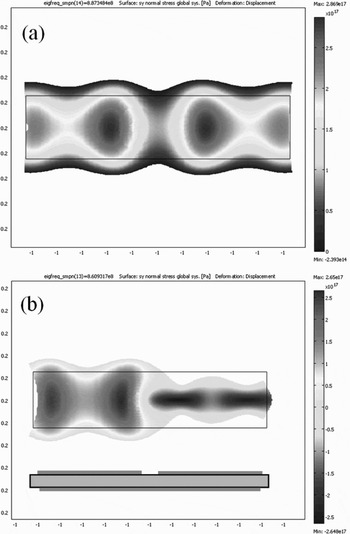
In a similar rectangular plate, the fundamental thickness extensional resonance mode is simulated in Fig. 4(a). The simulation is performed in 2D (cross section of the plate) in order to reduce computational complexity. As seen, this mode shape is symmetric relative to the X = 0 axis. The dual anti-symmetric mode shape is shown in Fig. 4(b). Similar to the lateral mode case, in this mode shape the strain field developed in the two halves of the structure is out-of-phase. Accordingly, the inset picture of Fig. 4(b) is the optimized electrode pattern to excite and couple the 2 modes. This pattern is the same as the electrode design commonly used in low-frequency MCFs. It should be noted that contrary to the situation in an MCF, in a TPoS structure the excitation force is only introduced inside the piezoelectric film and not the entire body of the resonant structure.
Dual fundamental thickness resonance mode shapes of a silicon plate in 2D.

One concludes that the same electrode pattern used for a lateral mode filter can potentially excite the coupled thickness modes of the structure. In practice, it was observed that the pattern employed for a lateral-mode device is not efficient for operation of a thickness mode filter. The problem is the excessive number of spurious modes excited by a simple two-piece electrode pattern. In other words, this pattern is not efficient in constraining acoustic energy in the two targeted modes on a relatively large suspended plate.
One alternative design to alleviate the problem is an interdigitated top electrode pattern (Fig. 5). With this design, the targeted anti-symmetric mode shape is extended in the lateral direction, meaning that in the mode shape of Fig. 4(b) the number of regions with alternating strain will increase. Using FEA simulations, multiple mode shapes from this family can be identified in a structure. These modes are different in the number of strain-alternating regions developed in the structure.
Schematic viewgraph of the interdigitated electrode pattern for monolithic thickness mode TPoS filters.

One of these modes, which can be excited by the electrode pattern depicted in Fig. 5, is shown in Fig. 6. Since the resonance frequency of each of these modes is slightly different from the others, the frequency spacing or, in other words, the BW of the 2nd-order thickness mode filter can be designed by changing the number of fingers covering a suspended plate. From FEA simulation results, it is predicted that by increasing the number of fingers the frequency spacing between the two coupled modes increases. The relevance of this prediction will be evaluated by experimental measurements in the following section.
Simulated thickness resonance mode shape of a silicon plate in 2D with 4 strain-alternating regions.

In contrast with FBAR filters, in a TPoS device the strain field developed in the film, and consequently the electromechanical coupling for the fundamental thickness mode, is not usually the strongest. This is because the piezoelectric layer comprises only a fraction of the structure thickness. Therefore, the mode number, for which the insertion loss is the lowest, depends on the thickness ratio between the piezoelectric film and the substrate. For example, in a thickness mode TPoS filter with an approximately 2:1 thickness ratio between the silicon layer and the piezoelectric film, the 3rd-order thickness mode is more likely to have the lowest insertion loss. In contrast, with a thickness ratio of 1:1, the second harmonic mode has the largest electromechanical coupling. It is also noteworthy that for a TPoS device, even mode numbers can be excited as opposed to an FBAR where only odd mode orders could appear.
III. EQUIVALENT ELECTRICAL MODEL
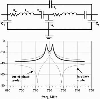
Mechanically coupled resonator systems are represented variously in electrical domain. One common representation of these systems is shown in Fig. 7 [Reference Wang and Nguyen15]. Individual resonators in this circuit are modeled as series RLC tanks coupled through a coupling shunt capacitor (Cc). This capacitor represents the stiffness of the coupling element. Rm, Lm, and Cm are the motional resistance, inductance, and capacitance of the resonator and Cs is the static capacitance of the input and output electrodes shunted to ground. Cf represents feedthrough capacitance.
Equivalent electrical model for a 2nd-order coupled resonator filter and a typical corresponding frequency response.

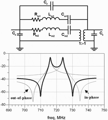
The same model can characterize monolithic filters. However, unlike mechanically coupled resonators no discrete coupling element is identified in a monolithic filter; rather it is acoustic energy that is coupled through the substrate. In the electrical model of Fig. 7, the frequency of the in-phase mode is always lower than the frequency of the out-of-phase mode (assuming a positive value for Cs). This is not usually the case for a monolithic filter and therefore two notches will appear before and after the filter passband in the frequency response, which can only be generated if the value chosen for the coupling capacitor is negative (alternatively a coupling inductor can be used [Reference Dworsky16]). A more intuitive way of modeling the frequency response is to use an ideal transformer in the model that accounts for the phase inversion in one of the modes (Fig. 8) [Reference Onoe, Jumonji and Kobori17]. In this way the frequency of the two modes can be controlled independently. If the frequency of the tank with mode inversion is chosen to be lower than the frequency of the other tank, the two notches will appear in the frequency response (Fig. 8).
Alternative equivalent electrical model for a 2nd-order monolithic filter and a typical corresponding frequency response.

IV. IMPLEMENTATION AND RESULTS
TPoS filters are fabricated in a 5-mask low-temperature process and details of the process flow are discussed elsewhere [Reference Ho, Abdolvand and Ayazi14]. A thin ZnO layer is chosen as the piezoelectric material on 4–5-μm-thick SOI substrates. Fabricated monolithic TPoS filters were tested on a Suss RF probe station using Agilent E5071B and E8364B network analyzers in atmospheric pressure. Two-port s-parameters were measured using calibrated GSG probes and saved as frequency plots and touchstone (.s2p) data files.
The first presented result is measured from a lateral mode device with a drawn center-to-center finger pitch of 16 μm (Fig. 9).
SEM of a 2-pole monolithic TPoS filter in which dual high-order lateral extensional mode shapes of the resonant structure are coupled (finger pitch = 16 μm).

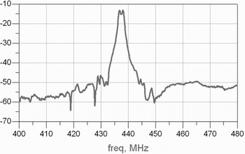
The center frequency (fc) of the filter is at ~440 MHz and the frequency spacing between the 2 resonance peaks is ~1.2 MHz. Therefore, the filter Q (defined as fc/BW) is ~300 (Fig. 10). The termination impedance is set to 500 Ω for this measurement and the out-of-band rejection is ~40 dB (a very large value considering the order of the filter).
Measured frequency response of the lateral monolithic TPoS filter shown in Fig. 9.

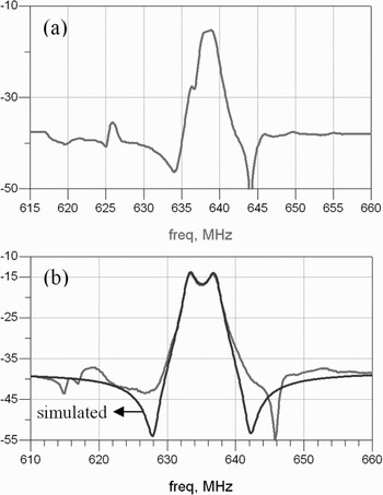
The frequency response plots of Fig. 11 are measured from two different monolithic filters with a center frequency at ~635 MHz. These results show how the BW of a lateral monolithic filter can be designed by changing the length of the device. The finger pitch in these two devices is 10 μm. The plot presented in Fig. 10(a) is measured from a 50-μm–long device and the plot in Fig. 10(b) is from a 35-μm-long device. As expected, the BW of the filter is increased as the length of the device reduces. However, one should notice that by decreasing the length of the device (assuming the same number of fingers) the total area covered by electrodes (actuation area) is reduced. Therefore, to design low IL filters with relatively wide BW the number of fingers should be increased in order to maintain a large actuation area.
Measured and simulated frequency responses of 2 lateral TPoS filters at 635 MHz.

Unlike the frequency response plot presented in Fig. 10, the 2 notches before and after the filter passband are more prominent in the results shown in Fig. 11. The reason is that the profile of the notches is dependent on the feedthrough impedance of the filter (equivalent impedance of the feedthrough capacitance at center frequency). For lower frequencies where the feedthrough impedance is large (the signal floor is low), the 2 notches almost disappear in the noise floor, whereas at higher frequencies the effect of the feedthrough capacitance is visible. Table 1 summarizes the value of individual components used to plot the simulated response of Fig. 10(b). The model introduced in Fig. 7 is used for generation of the plot. As discussed before, a negative coupling capacitance or in other words a coupling inductor (Lc) is considered to predict the notches. To further improve the model, one can include the effect of dielectric loss in the piezoelectric film by adding shunt resistances to ground in the input and output ports. Asymmetry of the response can be modeled by a capacitor in the inductive coupling branch as well [Reference Onoe, Jumonji and Kobori17].

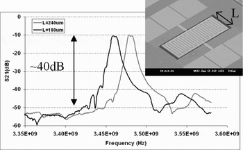
Thickness mode TPoS filters are also fabricated and characterized. The thickness ratio of silicon to ZnO layers is ~4 and the mode number with the minimum IL was measured to be the 5th mode at ~3.5 GHz. The overlapped plots of Fig. 12 are measured from 2 similar adjacent devices that only differ in the length of the suspended plate (labeled as L on the SEM picture).
Measured frequency response plots and the SEM picture of 3.5 GHz thickness mode monolithic TPoS filters.

The frequency response plots replicate each other with a frequency offset of <20 MHz. The filter BW is ~8.5 MHz, resulting in a filter Q of >400. The filters are inductively tuned and terminated to 250 Ω. The measured isolation of >40 dB is remarkably large for a 2nd-order filter spanning a small area of less than 500 μm × 250 μm.
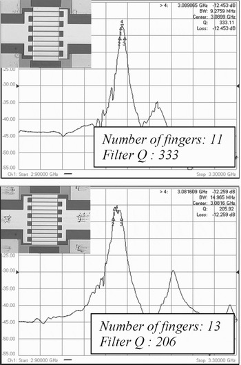
In a different experiment, the number of top electrode fingers patterned on the same suspended plate is varied and the frequency response of each device is measured. The results are consistent with the trend predicted in Section II and the BW of filters with a larger number of fingers is increased (at a constant center frequency of ~3.1 GHz). Table 2 summarizes the measured BW for four different filters and shows the corresponding number of fingers. Two of the frequency response plots are shown in Fig 13.
Measured frequency response plots and optical viewgraphs of 2 thickness mode monolithic TPoS filters with different number of fingers.

BW of thickness mode filters with identical resonant structure and different number of fingers.

V. CONCLUSION
Miniaturized filters that utilize dual lateral- and thickness-extensional resonance modes of a free-standing thin-film piezoelectric-on-silicon composite structure are designed and fabricated. Dual high-order lateral extensional resonance modes of a rectangular plate are excited and coupled to achieve dispersed-frequency 2nd-order RF filters on a single substrate. The BW of these filters was shown to be controlled by the length of the structure. An interdigitated 2-port top electrode pattern was found to be effective for excitation of dual thickness resonance modes of a suspended plate. The number of fingers in the interdigitated pattern was used to effectively control the BW of these filters. By changing the length of the structure, a small shift in the frequency of the thickness mode filters was also achieved. Narrow BW lateral mode filters in low RF range and thickness mode filters with Q’s in the range of 150–900 were demonstrated at ~3 GHz. Preliminary results prove that narrow BW filters with large out-of-band rejection can be fabricated in small footprints using the introduced mode coupling technique. These filters are suitable for multi-band channel-select filtering in the new generation of wireless equipment.
 Reza Abdolvand received his B.S. and M.S. degrees in electrical engineering from Sharif University of Technology, Tehran, Iran, in 1999 and 2001, respectively. He then joined the Georgia Institute of Technology, Atlanta, GA, in 2002, where he received his Ph.D. degree in the School of Electrical and Computer Engineering in 2008.
Dr. Abdolvand is now with the School of Electrical and Computer Engineering at Oklahoma State University as an assistant professor (starting from August 2007). His research interests lie in the area of micro/nano-electromechanical systems with a special focus on design, fabrication, and characterization of integrated micro-resonators with applications in RF circuits and resonant sensors. He holds 5 issued and pending patents in the field of micro-machining techniques and resonant micro-devices.
 Farrokh Ayazi received his B.S. degree in electrical engineering from the University of Tehran, Iran, in 1994 and his M.S. and Ph.D. degrees in electrical engineering from the University of Michigan, Ann Arbor, in 1997 and 2000, respectively. He joined the faculty of the Georgia Institute of Technology in December 1999, where he is now an associate professor at the School of Electrical and Computer Engineering. His research interests are in the areas of integrated micro- and nano-electromechanical resonators, IC design for MEMS and sensors, RF MEMS, inertial sensors, and microfabrication techniques.
Prof. Ayazi is a 2004 recipient of the NSF CAREER Award, the 2004 Richard M. Bass Outstanding Teacher Award (determined by the vote of the ECE senior class), and the Georgia Tech College of Engineering Cutting Edge Research Award for 2001–2002. He received a Rackham Predoctoral Fellowship from the University of Michigan for 1998–1999. He is an editor for the IEEE/ASME Journal of Microelectromechanical Systems, and serves on the technical program committees of the IEEE International Solid State Circuits Conference (ISSCC).