Introduction
Electric-field-induced emission of electrons is a physical phenomenon that utilizes a strong electric field to lower the surface energy barrier such that electrons can tunnel into a vacuum without the assistance of thermal excitation. Many types of electron optical instruments require a point electron source that can produce an electron probe with high brightness and monochromaticity for imaging and analysis of samples under investigation. Over the past two decades, research on nanostructures of materials has resulted in numerous innovations of nanoscale electron emission structures including single atom tips, nanotubes, and nanowires.
Field emission is well described by the Fowler–Nordheim equation, Reference Fowler and Nordheim1 developed in 1928, in which the electron emission current density (in A/m2) is obtained as:
 $$J = a{{{F^2}} \over \phi }exp\left( { - b{{{\phi ^{3/2}}} \over F}} \right)$$
,
where
 $a\, = \,1.54\,\, \times \,\,{10^{ - 6}}$
A eV V–2,
 $b\, = \,6.83\, \times \,{10^9}$
V m–1 eV–3/2, ϕ is the work function (in eV) of the emission surface, F is the local electric field (in V m–1), and β is a dimensionless field enhancement factor defined as
 $F = \beta {V \over r}$
, where V is the applied extraction voltage and r is the radius of curvature of the sharp tip from which electrons are emitted. The strength of the electric field F depends on the geometrical sharpness of the emitter tip.
Reference Rezeq, Pitters and Wolkow2
Cold-field emission provides the highest brightness and monochromaticity among various electron sources. This is especially important for electron optical applications. In the past, only refractory metals such as W, Mo, and Ta were considered field-emission materials. This was due to several factors.
First, mature needle etching processes were only available for these metals to produce the required tip sharpness. Second, thermal flashing, an established procedure to remove the adsorbates on the emitter by controlled heating, was effective to produce an oxide-free clean surface for these metals. For other materials, including carbon or compounds, there is still no effective procedure available that guarantees formation and subsequent cleaning of a sharp needle thinner than 100 nm. Reference Oshima, Rokuta, Itagaki, Ishikawa and Cho3,Reference Swanson and Schwind4 Since its first application in the scanning transmission electron microscope (STEM) to image single atoms in the 1960s, tungsten continues to be the only field-emission electron source for electron microscopes in industrial applications where it delivers the highest brightness and service life. Reference Crewe, Wall and Langmore5 However, even for the most refined electron source made of a single crystal of tungsten with its (310) facet as the emission surface denoted as W(310), its applications are still limited by its poor emission stability (5–10%) and large energy spread (0.3–0.4 eV).
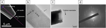
The recent emergence of nanoscale material structures has created an exciting opportunity for various compounds to be explored for field-emission applications. Nanostructures, including nanotubes, nanowires, and nanotips possess natural sharpness with tip dimensions of just a few tens of nanometers or less. The small size induces high field enhancement that could generate field-emission currents over a microampere under low extraction voltages of only a few tens of volts. Reference Smith, Cox and Silva6,Reference Wang, Chen and Peng7 Among recent advances, carbon nanotubes, noble atom nano-tips, and LaB6 nanowires have been investigated in detail with regard to source brightness, beam monochromaticity, and current stability. Figure 1 shows two such nanostructures developed for field-emission applications. Figure 1a is a nanostructure utilizing a single LaB6 nanowire attached to a W needle as the support substrate for ease of handling. Reference Zhang, Tang, Yuan, Yamauchi, Suzuki, Shinya, Nakajima and Qin8 A high-resolution transmission electron microscope (TEM) image of a typical LaB6 nanowire is depicted in Figure 1b—the nanowire is single-crystalline with a clean surface (indicated by arrow) and is grown along 〈001〉. Figure 1c shows a single carbon nanotube emitter (indicated by arrow) that is sticking out of a carbon fiber. Reference Zhao, Zhang, Zhang, Yang, Zhou, Qin and Tang9 The electron diffraction pattern is given in Figure 1d, with which the atomic structure (chirality or chiral indices) of the carbon nanotube could be identified for structure–property studies. Reference Zhao, Zhang, Zhang, Yang, Zhou, Qin and Tang9
(a) Scanning electron microscope image of a LaB6 nanowire emitter composed of a single LaB6 nanowire welded onto the tip of a W needle. Reference Zhang, Tang, Yuan, Yamauchi, Suzuki, Shinya, Nakajima and Qin8 C-bonding indicates a carbon pad deposited to fix the LaB6 nanowire onto the W needle. (b) Transmission electron microscope (TEM) image of a LaB6 nanowire showing perfect crystallinity and a clean surface as indicated by the arrow. Reference Zhang, Tang, Yuan, Yamauchi, Suzuki, Shinya, Nakajima and Qin8 (c) TEM image of a carbon nanotube emitter with a single multiwalled carbon nanotube (indicated by arrow) extruded out of a carbon fiber. Reference Zhao, Zhang, Zhang, Yang, Zhou, Qin and Tang9 (d) A nanobeam electron diffraction pattern recorded from the multiwalled carbon nanotube emitter revealing the chiral indices for each of the five walls. Reference Zhao, Zhang, Zhang, Yang, Zhou, Qin and Tang9

Many effective experimental methods have been developed for fabrication of films with various nanostructures on a variety of substrates. Reference Fan, Werner and Zacharias10–Reference Zheng, Yang, Xie, Qu, Liu and Li12 It has been shown that a film with a high density of individual field emitters could outperform the best thermionic emitters in terms of emission current density for high-power planar electron source applications. Reference Spindt, Holland and Stowell13,Reference Schwoebel, Spindt and Holland14 In low-current density applications such as field emission displays and lamps, each individual nano-emitter is expected to emit a low current of only a few nanoamperes. Even insulating material structures can be used as field-emission planar sources, where the conduction of electrons occurs through surface states. Reference Forbes15 Emission stability for these planar sources is determined from the temporal variation of the total emission current over a fixed emitter area. Fluctuations in emission current due to individual emitters can thereby be statistically compensated and an average constant total emission current can be obtained. Reference Fan, Chapline, Franklin, Tombler, Cassell and Dai16 High-temperature flashing for surface cleaning is not normally performed for these emitters, and the operating vacuum is usually maintained at high vacuum (∼10–7 Torr or 1.33 × 10⁻⁵ Pa), where chamber baking is usually not performed. A series-inserted ballast resistor could also be used to reduce the emission noise if the particular application is not beam energy sensitive. Reference Sun, Yeow and Jaffray17 There are several reviews in the literature covering research progress in this field. Reference Zhai, Li, Ma, Liao, Wang, Fang, Yao, Bando and Golberg18–Reference Fang, Bando, Gautam, Ye and Golberg20
While performance of electron emission measured from a nanostructured film reflects the collective properties of multiple emitters, electron emission from a single nanostructure provides more insightful information such as the crystallographically dependent field-emission pattern, source brightness, beam monochromaticity, and emission current stability. Reference Zhang, Zhang, Zhao, Tang, Zhou and Qin21–Reference Yuan, Zhang, Tang, Shinya, Nakajima and Qin26 The most direct application for an individual point emitter is as the electron source for electron optical instruments, including the TEM, the scanning electron microscope (SEM), electron-beam lithographic systems, and point projection microscopes.
The brightness of an electron source is defined as B = I/(ΩVs
v), where I is the emission current,
 $\Omega$
is the solid angle of divergence of the emitted electron beam, V is the acceleration voltage applied to the emitted electron, and s
v is the area of the virtual source. It reflects the geometrical contribution from the virtual source to the final electron probe size in an electron optical system producing a fine electron probe.
Reference Shimoyama and Maruse27,Reference Bronsgeest, Barth, Swanson and Kruit28
Monochromaticity is measured as the energy spread of the electrons emitted from the source surface. In a probe-forming system, the monochromaticity determines the electron-beam broadening attributed to chromatic aberration of the probe-forming lens.
Reference Schwind, Mager and Swanson29
The Fowler–Nordheim equation indicates that the only way to increase source brightness and monochromaticity simultaneously is to lower the work function of the emission surface.
Reference de Jonge, Allioux, Oostveen, Teo and Milne30
Emission stability also depends on the vacuum level. It is usually categorized into long-term stability and short-term stability, manifested as current decay and as high-frequency noise, respectively.
Reference Swanson and Martin31
In this article, we summarize recent advances in the research and development of field-emission of electrons using a single nanostructure, in particular a single nanowire, to fabricate a field-emission electron source for applications in electron microscopes. Emphasis on the performance parameters is placed on source brightness, emission stability, and beam monochromaticity in comparison with the contemporary W(310) tip. An example of a single LaB6 nanowire field-emission electron source installed in an SEM for imaging and analysis of materials is also described.
Source brightness
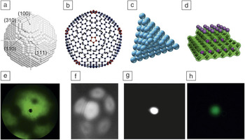
For a needle emitter such as the W(310) tip widely used in contemporary electron microscopes, the tip cap is in the form of a smooth hemisphere, and electrons are emitted from the entire hemisphere. Figure 2 schematically compares the atomic structure of a few typical field-emission nanostructures and their corresponding field-emission patterns, including (a) a W(310) tip, Reference Rahman, Onoda, Imaizumi and Mizuno32 (b) a carbon nanotube with a closed end, Reference Nakahara, Kusano, Kono and Saito33 (c) a single-atom tip of Pd on W,34 and (d) a single-crystalline LaB6 nanowire. Reference Zhang, Tang, Yuan, Yamauchi, Suzuki, Shinya, Nakajima and Qin8 For the W(310) tip, the distribution of emission intensity depends on the crystallographic distribution of the work function that is governed by local atomic densities, as shown in Figure 2a. Reference Yamamoto35 Even for a nanostructure field emitter, the electron emission usually takes place only within a region on the emitter tip that is much smaller than the tip itself. The emission sites of a carbon nanotube emitter are carbon pentagons located at the tip vertices (Figure 2b), Reference Nakahara, Kusano, Kono and Saito33 those of a single-atom tip are the atomic Pd pyramid at the apex of a refractory tungsten metal needle (Figure 2c), Reference Hwang, Kuo, Chang and Tsong34 and those of a LaB6 nanowire emitter are a cluster of La atoms located at the tip apex (Figure 2d). Reference Zhang, Tang, Yuan, Yamauchi, Suzuki, Shinya, Nakajima and Qin8 Their corresponding field-emission patterns are shown in Figure 2e–h. It should be noted that, for the W(310) (Figure 2e) Reference Rahman, Onoda, Imaizumi and Mizuno32 and carbon nanotube (Figure 2f) Reference Yamashita, Matsuda, Kona, Mogami, Komaki, Murata, Oshima, Kuzumaki and Horiike36 emitters, the field emission shows faceted patterns, while only a single emission spot is observed for the single-atom Pd tip (Figure 2g) Reference Hwang, Kuo, Chang and Tsong34 and the LaB6 nanowire (Figure 2h) Reference Zhang, Tang, Yuan, Yamauchi, Suzuki, Shinya, Nakajima and Qin8 emitters. A nanostructure emitter can deliver an emission brightness much higher than that of the W(310) emitter because its smaller emission area generates a smaller virtual source size. Reference Ishikawa, Cho, Rokuta and Oshima37 It should also be noted that the smaller emission area spreads out the electrons more quickly such that the space-charge and the Boersch effects that cause beam broadening with increasing current density are minimized, thus achieving higher maximum brightness. Reference Kruit, Bezuijen and Barth38 Although this higher brightness can improve electron microscope resolution, fully utilizing the high brightness imposes new engineering design requirements for the electron gun. Reference Scheinfein, Qian and Spence39,Reference Jensen40
(a–d) Atomic structure model illustrating the field-emission site. (a) A W(310) emitter with various crystallographic facets indicated. Reprinted with permission from Reference Reference Rahman, Onoda, Imaizumi and Mizuno32. © 2008 Elsevier. (b) A carbon nanotube with a closed cap with carbon pentagons colored red. Reprinted with permission from Reference Reference Nakahara, Kusano, Kono and Saito33. © 2009 Elsevier. (c) A pyramidal Pd single-atom tip covering a W needle. Reprinted with permission from Reference Reference Hwang, Kuo, Chang and Tsong34. © 2010 The Electrochemical Society. (d) A LaB6 nanowire with La and B atoms colored purple and green, respectively. Reference Zhang, Tang, Yuan, Yamauchi, Suzuki, Shinya, Nakajima and Qin8 (e–h) Field-emission pattern from the previously discussed emitters. (e) The W(310) tip. Reprinted with permission from Reference Reference Rahman, Onoda, Imaizumi and Mizuno32. © 2008 Elsevier. (f) Carbon nanotube. Reprinted with permission from Reference Reference Yamashita, Matsuda, Kona, Mogami, Komaki, Murata, Oshima, Kuzumaki and Horiike36. © 2002 Elsevier. (g) Single-atom tip. Reprinted with permission from Reference Reference Hwang, Kuo, Chang and Tsong34. © 2010 The Electrochemical Society. (h) LaB6 nanowire. Reference Zhang, Tang, Yuan, Yamauchi, Suzuki, Shinya, Nakajima and Qin8

Methods for measurement of the virtual source size include (1) calculation of the electron trajectory from knowledge of the exact tip geometry, Reference Qian, Scheinfein and Spence41 (2) measurement of the coherent length using interferometry, Reference Chang, Kuo, Hwang and Tsong42 (3) measurement from a TEM image of the virtual source, Reference Fransen, Overwijk and Kruit43 and (4) direct measurement from a field-ion microscope (FIM) image. The FIM method is highly effective when the atomic structure of the emitter tip is imaged on the screen such that the image magnification is well calibrated. Using the FIM method, the lower boundary of the source brightness of a LaB6 nanowire emitter is 1.6 × 10¹¹ A/m2/sr/V, which is two orders of magnitude higher than that of the W(310) emitter used in commercial field-emission electron microscopes. Reference Zhang, Tang, Yuan, Yamauchi, Suzuki, Shinya, Nakajima and Qin8 Demonstration of a carbon nanotube emitter used in a TEM clearly showed a higher degree of beam coherence resulting from higher source brightness. Reference Houdellier, Masseboeuf, Monthioux and Hytch44 When a LaB6 nanowire emitter is used to replace the original W(310) emitter in a field-emission SEM under the same imaging conditions, it produced a probe with a much larger current, as described later in this article.
Emission stability
Another dramatic change in utilizing a nano-emitter as compared to the traditional metal needle emitter is the much slower emission decay due to residual gas adsorption. Residual gas molecules could adsorb onto the emitter shank when electrostatic forces exerted on the emitter during field emission draw gas molecules toward the tip area through field-assisted diffusion. The gas molecules could eventually cover the apical emitting surface and cause either an increase or decrease in emission current, depending on the direction of dipoles formed between the gas molecules and the metal atoms underneath. Reference Yamamoto, Fukuhara, Okano and Saito45,Reference Christmann46
However, the binding between the gas molecules and metal surface is usually rather weak such that the gas molecules could be desorbed by the emission current or the strong electric field at the emitter tip (i.e., the adsorption and desorption processes can take place simultaneously), which accounts for fluctuations in the emission current. Reference Naumovets and Vedula47 When an extremely high vacuum of 10–12 Torr (1.33 × 10⁻¹⁰ Pa) is applied, the onset of these emission instabilities can be postponed by a few hours immediately after emitter surface cleaning. Reference Kasuya, Katagiri, Ohshima and Kokubo48,Reference Kasuya, Katagiri and Ohshima49 In contrast, a nanowire can generate a constant emission current at room temperature in a moderate ultrahigh vacuum of 10–9 Torr (1.33 × 10⁻⁷ Pa), where the majority of residual gas is H2. Reference Zhang, Tang, Yuan, Yamauchi, Suzuki, Shinya, Nakajima and Qin8
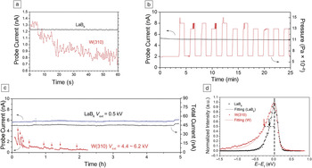
As an example, the resistance to H2 contamination for a LaB6 nanowire is shown in Figure 3a–c. Reference de Jonge, Allioux, Oostveen, Teo and Milne30 The short-term noise level is as low as 0.1% (Figure 3a), which rivals that of thermionic emitters operating at high temperatures above 1600°C. The low noise eliminates the necessity of a noise canceler when a LaB6 nanowire is used as the electron source in an SEM (Figure 3c). The probe current from the LaB6 nanowire emitter was stable even when tested under an intentional H2 gas leak into the vacuum chamber, as illustrated in Figure 3b. In addition, the LaB6 nanowire emitter also exhibited promising long-term stability of the probe current in comparison to a W(310) emitter installed in the same SEM (Figure 3c). The room-temperature resistance to adsorption for a nanowire is a morphology-dependent unique property, unlike its bulk counterpart. Reference Yamamoto, Hosoki, Fukuhara and Futamoto50–Reference Futamoto, Hosoki, Okano and Kawabe52
(a) Short-term noise profile of a LaB6 nanowire emitter and a W(310) emitter. Reference Zhang, Tang, Yuan, Yamauchi, Suzuki, Shinya, Nakajima and Qin8 (b) Probe current of a LaB6 nanowire emitter under intentional leakage of H2 gas, causing the chamber pressure to vary between 0.5 × 10⁻⁹ and 1.0 × 10⁻⁹ Torr (0.66 × 10⁻⁷ and 1.33 × 10⁻⁷ Pa, respectively). Reference Zhang, Tang, Yuan, Yamauchi, Suzuki, Shinya, Nakajima and Qin8 (c) Long-term probe current stability comparing a LaB6 nanowire emitter and a W(310) emitter installed in the same scanning electron microscope as the electron source. Red arrows in the W(310) profile indicate extraction voltage (V ext) changes in the measurement. Reference Zhang, Tang, Yuan, Yamauchi, Suzuki, Shinya, Nakajima and Qin8 Both total current (right axis) and probe current (left axis) are shown in the figure. The LaB6 nanowire emitter has superior emission stability over the W(310) emitter, showing no decay at constant voltage over long operation duration. Reference Zhang, Tang, Yuan, Yamauchi, Suzuki, Shinya, Nakajima and Qin8 (d) Energy spread for the LaB6 nanowire and W(310) emitters. Reference Zhang, Tang, Yuan, Yamauchi, Suzuki, Shinya, Nakajima and Qin8 The red and black arrows indicate the lower value of the energy spread at half of maximum. The horizontal dashed line shows the energy spread relative to the Fermi energy at half maximum. The Fowler–Nordheim fitting Reference de Jonge, Allioux, Oostveen, Teo and Milne30 was performed for both energy profiles and shows good agreement with the room-temperature field-emission mechanism. Note: E, energy; E f, Fermi energy.

The following possible mechanisms were proposed to explain these phenomena. For a carbon nanotube with a closed cap, the lack of dangling bonds on the graphene layer prevents chemisorption. Reference de Jonge, Allioux, Oostveen, Teo and Milne53 For a single-atom tip, the strong electric field concentrated on the noble metal pyramid field-desorbs the attached gas molecules. Reference Akamine, Fujiwara, Oshima and Cho54 In the case of a LaB6 nanowire, it is believed that the reactive valence electrons from surface La atoms are localized by the B atoms underneath.
Beam monochromaticity
When a strong electric field is applied to the surface of an emitter, the surface-energy barrier is lowered near the surface-vacuum-energy level. A monochromatic electron beam would be the result if only electrons at the exact Fermi level tunneled out. In reality, emitted electrons experience energy broadening as they have energy both above and below the Fermi level. The broadening on the higher energy side is temperature dependent. Electrons thermally activated above the Fermi level would tunnel through an even lower barrier, therefore they have a higher tunneling probability. The electrons below the Fermi level would tunnel through an energy barrier higher than that for electrons at the Fermi level; therefore, they have a lower, yet not negligible, tunneling probability.
Such lower-energy broadening depends on the surface work function—the lower the work function, the lower the energy broadening. Therefore, the monochromaticity of a field-emitted electron beam is dependent on the material chemistry rather than the tip morphology. Compared to the W(310) surface with a work function of 4.5 eV, carbon nanotubes have a higher work function of 5.0 eV, and the noble metals have even higher work functions; Pt for instance has a work function of 5.6 eV. The energy spread in the electron beam produced by both a carbon nanotube and a single-atom tip is slightly larger than that from a W(310) emitter. Reference de Jonge, Allioux, Oostveen, Teo and Milne30,Reference Rokuta, Kuo, Itagaki, Nomura, Ishikawa, Cho, Hwang, Tsong and Oshima55,Reference Binh, Purcell, Garcia and Doglioni56 On the other hand, the La-B dipole layer at the apical surface of a LaB6 nanowire results in a low work function of only 2.3 eV. Reference Uijttewaal, de Wijs and de Groot57 As shown in Figure 3d, the energy spread of a LaB6 nanowire emitter is measured at 0.24 eV (full width at half maximum), with 0.12 eV due to the lower energy side and 0.12 eV due to the higher energy side.
Thermal broadening at the higher energy side fits the Fowler–Nordheim theory well at room temperature (20°C). The lower energy broadening for the LaB6 nanowire emitter is 50% smaller than that of the W(310) emitter at the same current density due to a much lower surface work function for LaB6. The smaller energy spread of the LaB6 nanowire emitter is especially important for low-energy electron-beam applications where the resolution is limited by chromatic aberrations of the imaging lens. Reference Krivanek, Chisholm, Nicolosi, Pennycook, Corbin, Dellby, Murfitt, Own, Szilagyi, Oxley, Pantelides and Pennycook58 For electron energy-loss spectroscopy, a smaller energy spread in the primary electron beam also leads to higher energy resolution. Even for an electron gun equipped with a monochromator, a smaller energy spread in the primary beam yields a higher beam brightness and a greater signal/noise ratio could be maintained post energy-filtering. Reference Krivanek, Lovejoy, Dellby, Aoki, Carpenter, Rez, Soignard, Zhu, Batson, Lagos, Egerton and Crozier59
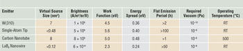
Table I summarizes these key performance parameters of various nanostructured field emitters previously described, including the single LaB6 nanowire, single-atom tip, single-carbon nanotube, and the contemporary W(310) tip.
Field-emission electron source performance of nanostructured emitters. Reference Oshima, Rokuta, Itagaki, Ishikawa and Cho3,Reference Swanson and Schwind4,Reference Zhang, Tang, Yuan, Yamauchi, Suzuki, Shinya, Nakajima and Qin8,Reference de Jonge, Allioux, Oostveen, Teo and Milne30,Reference Chang, Kuo, Hwang and Tsong42,Reference Kasuya, Katagiri, Ohshima and Kokubo48,Reference Kasuya, Katagiri and Ohshima49

Note: RT, room temperature.
Imaging with nanowire electron sources
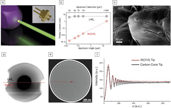
Due to the high cost and limited availability of dedicated electron microscopes for performance testing, more data is needed to evaluate the nanostructure emitters for industrial applications. Nonetheless, installation and evaluation of performance have been reported for both the single carbon nanotube emitter Reference Houdellier, Masseboeuf, Monthioux and Hytch44 and the LaB6 nanowire emitter. Reference Zhang, Tang, Yuan, Yamauchi, Suzuki, Shinya, Nakajima and Qin8 Figure 4a depicts the electron emission site of a LaB6 nanowire emitter with the inset showing an actual assembled electron microscope emitter with a LaB6 nanowire tip. Reference Zhang, Tang, Yuan, Yamauchi, Suzuki, Shinya, Nakajima and Qin8 When installed in an SEM, the probe current from the LaB6 nanowire emitter could be 3000× larger than that from a W(310) emitter, as shown in Figure 4b. Reference Zhang, Tang, Yuan, Yamauchi, Suzuki, Shinya, Nakajima and Qin8 Using such a LaB6 nanowire emitter, an SEM image of part of an uncoated spider at a beam acceleration of 400 V is displayed in Figure 4c. It should also be noted that, when an object is imaged in the SEM using a LaB6 nanowire electron source, the image exhibited a much lower noise level compared to that taken with a W(310) emitter, as shown in Figure 4d (upper half of image and lower half of image, respectively). Reference Zhang, Tang, Yuan, Yamauchi, Suzuki, Shinya, Nakajima and Qin8 Figure 4e shows a TEM image of a condenser aperture showing interference rings recorded by using a carbon-cone emitter with a single carbon nanotube as the emitting element. Reference Houdellier, Masseboeuf, Monthioux and Hytch44 The line profiles of the TEM image acquired using the carbon nanotube emitter showed a larger coherent length compared with the image obtained from a W(310) emitter (Figure 4f). Reference Houdellier, Masseboeuf, Monthioux and Hytch44
Electron microscopy applications of nanostructured electron emitters. (a) Schematic showing the electron emission site of a LaB6 nanowire emitter to be the La atom cluster at the nanowire tip (the inset shows an assembled electron microscope emitter with a LaB6 nanowire tip). Reference Zhang, Tang, Yuan, Yamauchi, Suzuki, Shinya, Nakajima and Qin8 (b) When the aperture angle changes, the probe current of a scanning electron microscope (SEM) using a LaB6 nanowire emitter is stable in comparison to a W(310) emitter. Reference Zhang, Tang, Yuan, Yamauchi, Suzuki, Shinya, Nakajima and Qin8 (c) SEM image of part of an uncoated spider at a beam acceleration of 400 V using a LaB6 nanowire emitter. (d) SEM images taken without a noise canceler of the same object using (upper half of image) a LaB6 nanowire and (lower half of image) a W(310) emitter. Reference Zhang, Tang, Yuan, Yamauchi, Suzuki, Shinya, Nakajima and Qin8 (e) Transmission electron microscope image of a condenser aperture showing a large number of interference rings, a measure of the coherence of the electron source, recorded by using a carbon-cone emitter with a single carbon nanotube as the emitting element. Reprinted with permission from Reference Reference Houdellier, Masseboeuf, Monthioux and Hytch44. © 2012 Elsevier. (f) Line profiles of (e) using the carbon nanotube and the W(310) emitter, showing that the carbon nanotube emitter produced a more coherent electron beam. Reprinted with permission from Reference Reference Houdellier, Masseboeuf, Monthioux and Hytch44. © 2012 Elsevier.

Summary
Cold-field emission of electrons from a single nanowire provides the highest brightness and monochromaticity for an electron beam. This advantage is especially important for applications in electron optical instruments. Nanowire field emitters open up new opportunities for developing point electron sources with high brightness, small energy spread, and durable stability. The demonstrated performance clearly showed that a field emitter with both low work function and high surface stability is possible. The merits of high brightness and monochromaticity from cold-field emission and of high stability previously obtained only from thermionic emission can now be combined in the case of the LaB6 nanowire emitter.
Applications requiring point electron sources could benefit from a nanowire electron source as shown in the SEM examples. It is also anticipated that a nanowire electron source will be applied in emerging ultrafast electron diffraction and electron microscopy. Reference Kruger, Schenk and Hommelhoff60,Reference Aseyev, Weber and Ischenko61
Acknowledgments
The authors wish to acknowledge the Japan Science and Technology Corporation and the Nanotechnology Network Project of the Ministry of Education, Culture, Sports, Science, and Technology for financial support as well as the Hitachi High-Technology Corporation for their cooperation in this work.

Han Zhang is a senior researcher at the National Institute for Materials Science (NIMS), Japan. He received his bachelor’s degree from Tsinghua University, China, in 2002. He obtained his master’s and doctoral degrees from The University of North Carolina at Chapel Hill, in 2004 and 2007, respectively. His current research focuses on ultrahigh brightness electron source research and next-generation electron microscope development using nanostructures. His awards include the NIMS President’s Award for research development and the German Innovation Award—the Gottfried Wagener Prize—for distinguished advancement in materials science. Zhang can be reached by phone at +81-29-859-2295 or by email at zhang.han@nims.go.jp.

Jie Tang is a chief researcher and group leader of the Advanced Low-Dimensional Nanomaterials Group at the National Institute for Materials Science, Japan, a professor at Tsukuba University, Japan, and an adjunct professor at The University of North Carolina at Chapel Hill. She received her BEng degree in materials science from Tsinghua University, China, and her PhD degree in materials physics from Osaka University, Japan. Her research interests include high-pressure physics, electron-emission materials, and graphene supercapacitors for energy-storage applications. She has published more than 100 research papers and holds numerous patents. Tang can be reached by phone at +81-29-859-2728 or by email at tang.jie@nims.go.jp.

Jinshi Yuan is a postdoctoral researcher in the Advanced Low-Dimensional Materials Laboratory at the National Institute for Materials Science, Japan. He received his BS and MS degrees in materials science and engineering from Tsinghua University, China, and his PhD degree in materials science and engineering from the University of Tsukuba, Japan. His current research interests include synthesis, characterization, and applications of low-dimensional materials, including nanotubes, nanowires, and graphene for electron emission and energy storage, and charging and discharging dynamics and optimization of nanoporous electrodes for supercapacitors and batteries. Yuan can be reached by phone at +81-29-859-6842 or by email at yuan.jinshi@nims.go.jp.

Lu-Chang Qin is a professor in the Department of Physics and Astronomy at The University of North Carolina at Chapel Hill. He received his BS degree in physics from the University of Science and Technology of China, his MS degree in materials science and engineering from Northwestern University, and his ScD degree in materials science from the Massachusetts Institute of Technology. His research interests include the development and application of electron diffraction and microscopy techniques for materials characterization as well as nanostructured materials for electron-emission and energy-storage applications. He has published more than 150 papers. Qin can be reached by phone at 919-843-3575 or by email at lcqin@unc.edu.