I. INTRODUCTION
The development of the internet of things, smart cities or smart houses is expected to rely on Wireless Sensor Networks (WSN) composed of a huge number of interconnected electronic devices. Powering networks through cables or batteries may become almost impossible but mostly unpractical not to mention the adverse environmental effects [Reference Duroc and Kaddour1]. According to Koomey estimations, the total energy needed for a computational operation decreases by 50% each 18 months [Reference De Koomey, Berard, Sanchez and Wong2]. An example of this less powering evolution is the low-consumption passive radio frequency identification (RFID) tags: in 1997, the tag sensitivity was of −8 dBm, while nowadays it is only about −22 dBm [3]. Consequently in a near future, the harvesting solutions could completely satisfy the power needs of devices for the WSN. In this context, the use of passive tags could be very relevant because of their capabilities to integrate sensor functionalities while always benefiting from their advantages, i.e. wireless and battery-free [Reference De Donno, Catarinucci and Tarricone4–Reference Duroc and Andia Vera8]. With this motivation, new techniques of energy harvesting and methods to enhance the performances are a worldwide hot research topic [Reference Georgiadis and Collado9–Reference Popovic14]. These techniques have been addressed in the literature in a direct or indirect manner by considering the nonlinear behavior of electromagnetic energy harvesting (EEH) devices. Actually, it is possible to classify the treatment of these nonlinear behaviors in three main categories: (i) impedance-power dependence [Reference Roberg, Reveyrand, Ramos, Falkenstein and Popovic15–Reference Georgiadis, Andia and Collado17], (ii) harmonic generation [Reference Andia Vera, Duroc and Tedjini18–Reference Andia Vera, Duroc and Tedjini20], and (iii) waveform design [Reference Boaventura and Carvalho21–Reference Collado and Georgiadis24].
This paper proposes an approach to exploit these nonlinear phenomena using the passive RFID technology as the beacon for the implementation. The objective is to provide additional energy to the chip, allowing it to increase its sensitivity and consequently its read range. The proposed design combines the internal rectifier circuit of a commercial RFID chip operating at 868 MHz with an external rectifier circuit operating at 2.17 GHz both connected to a common single-feed dual-band antenna. The nonlinearity of each device is exploited in order to improve the global performance of the system, hereinafter the so-called RFID tag-rectenna (RFID-TR).
This paper is organized as follows. Section II presents the composition and operation of the RFID-TR system and the proposed method in order to enhance the conversion efficiency of rectifying devices. Section III details the optimized design of the composite system highlighting the exploitation of the nonlinear behavior of rectifiers. Section IV shows the evaluation results of the realized prototype and discusses the scope of the approach. Finally, Section V draws final conclusions and perspectives.
II RFID-TR SYSTEM
A) Architecture
The system architecture of the RFID-TR based on a double rectifier configuration is depicted in Fig. 1. The RFID-TR is mainly composed by: (i) the RFID section (including the so-called first rectifier) operating at 868 MHz, (ii) the EEH section (including the so-called second rectifier) operating mainly at 2.17 GHz, and (iii) a common dual-band antenna that serves as radiating element in order to communicate with the two external radio frequency (RF) sources.
Architecture of the RFID-TR system. The system consists of an EEH section (solid line), an RFID section (dash line), and a single-feed antenna.

The RFID section is in charge of the classic RFID link, including data information and energy harvesting. A distributed network integrated to the antenna matches the RFID chip impedance at 868 MHz. An EM4325 RFID chip (TSSOP-8 package) is used, because it offers a supplementary dc input pin in order to operate in battery-assisted power (BAP) mode [25, Reference Zheng, Hua, Zheng and Hong26]. The supplementary dc power allows the chip to enhance its activation sensitivity. The BAP mode will be later used in order to validate the proposed approach.
The EEH section is in charge of the generation of complementary power harvesting it from a 2.17 GHz signal combined with the third-harmonic generated by the chip [Reference Andia Vera, Duroc and Tedjini20] looking for an enhancement in the RF-to-dc conversion efficiency. A lumped matching network ensures the power transfer from the antenna, which has the RFID section connected, toward the rectifier diode at 2.17 GHz. An external RF source intended to belong to the Universal Mobile Telecommunications System (UMTS) band generates the 2.17 GHz signal. As proof of concept, it is worth noting that the 2.17 GHz signal does not consider any modulation. The rectifier element is an HSMS 2860 Schottky diode (SOT23 package) [27]. The integration of the double rectifier system allows it to inject the harvested energy by the EEH section into the RFID section enabling to increase the chip sensitivity and so to enhance the RFID-TR read range.
Finally, the double rectifier configuration, which intrinsically considers a double source operation (at 868 MHz and 2.17 GHz) as shown in Fig. 1, favors the powering performance of the RFID-TR because the design approach considers the nonlinear effects of each rectifier in a simultaneous operation. In other words, the described architecture aims to optimize the RFID-TR operation in terms of power generation in the EEH section and RFID communication exploiting the three nonlinear phenomena of diode-based circuits previously evoked and further detailed in the next paragraph.
B) Treating the nonlinearity of EEH devices for conversion enhancement
1) Impedance-power dependency
Due to the variable resistor and capacitor feature of rectifying diodes, the impedance of diode-based rectifier circuits is nonlinear dependent on the voltage [Reference Hagerty28]. This property led to consider a specific input power from which the design is optimized [Reference Roberg, Reveyrand, Ramos, Falkenstein and Popovic15–Reference Georgiadis, Andia and Collado17]. For the RFID-TR, the design should ensure: (i) the power transfer from the RFID reader toward the RFID chip at 868 MHz; (ii) the power transfer from the RFID chip toward the EEH section at the third harmonic (i.e. 2.604 GHz) in order to harvest this wasted power [Reference Andia Vera, Georgiadis, Duroc and Tedjini29]; and (iii) the power transfer from the 2.17 GHz source toward the EEH section. To achieve this operation, the matching networks of the RFID-TR system have to be optimized taking into account certain priorities: both RFID section and EEH section have to operate at −10 dBm at 868 MHz and 2.17 GHz, respectively. This value prioritizes the RFID chip activation [25].
2) Harmonic generation
The nonlinear i–v characteristic of a diode imposes a current signal to be composed by fundamental and harmonic components in function of the voltage operation. Most energy-harvesting circuits already contain a bandpass filter on the antenna input that permits the fundamental frequency to enter, but reflects the harmonics back into the energy harvester. This technique, very common in the high-efficiency energy harvester design, allows maximizing the conversion efficiency by confining all the higher order harmonics between the low-pass filter and the dc pass filter [Reference Yoo and Kain30]. Furthermore, harmonic treatment techniques such as the Class-E or Class-F rectifier [Reference Hagerty28] help to confine the energy carried by harmonics in order to optimize the conversion efficiency of rectifier circuits. The presented impedances to the rectifier circuit (at fundamental and harmonic frequencies) enable that the stored energy in the diode is not self-dissipated, but rather released to the load.
The harmonic treatment can be addressed in a design stage by simulation tools such as the harmonic balance [Reference Ladan and Wu19, Reference Andia Vera, Duroc and Tedjini20]. Figure 2 shows the normalized power spectral density (PSD) of the EM4325 RFID chip response measured using a similar method to the one reported in [Reference Andia Vera, Duroc and Tedjini20]. The setup considers the chip activation threshold power, the reader harmonics suppression, and the chip impedance matching at fundamental frequency as in common tags. At the chip activation threshold, the level of harmonic signals is significant at 1.736 GHz (second harmonic) and at 2.604 GHz (third harmonic), considering the scope of backscattering applications.
Normalized power spectral density of the tag response measured at the activation threshold of the chip under test [25].
Therefore, this paper proposes to exploit the chip harmonic generation in order to create a composite signal at the second rectifier input [Reference Andia Vera, Georgiadis, Duroc and Tedjini29]. This composite signal is composed by the third harmonic product of the RFID chip and the 2.17 GHz carrier wave (CW). The impact of the signal composition on the RF-to-dc conversion efficiency of the EEH section is studied in the next section.
3) Waveform dependency
When a rectifier circuit is excited simultaneously by more than one signal relative to a single carrier of the same average power, its nonlinear i–v characteristic can potentially lead to an enhanced RF-to-dc conversion efficiency. Indeed, a composite signal of a number of tones (i.e. a multi-harmonic) represents a signal with a time-varying envelope (i.e. the presence of instantaneous power peaks) and a certain peak-to-average-power-ratio (PAPR). The greater the PAPR is in the input signal, the greater is the RF-to-dc conversion efficiency of the rectifier. Furthermore, a time-varying envelope signal is capable to activate the rectifying devices for lower average input power levels compared with signals of constant envelope and the same average power. However at high-power levels, the PAPR decreases the conversion efficiency [Reference Boaventura and Carvalho21–Reference Collado and Georgiadis24, Reference Valenta and Durgin31].
Thereby, the combination of the CW at 2.17 GHz (i.e. a constant time envelope signal), and the ASK modulated third-harmonic product of the RFID chip produces a time-varying signal with higher PAPR than the one of a single CW signal. In the RFID-TR, the waveform dependency is then exploited by feeding the EEH section with a composite signal, i.e. a time-varying envelope signal that is used to boost the RF-to-dc conversion efficiency.
4) Summary and design requirements
The role of the RFID section is to ensure the RFID communication, and at the same time, to produce a third harmonic that will be exploited in the EEH section in order to improve the RF-to-dc conversion efficiency.
Actually, the harmonic reflection from the RFID chip toward the EEH section performs two tasks that drive the RFID-TR design: (i) to prevent losing the energy which is converted into harmonics that could impairs the efficiency of the RFID section; (ii) to redirect efficiently the harmonic power toward the EEH section. It is worth noting that the harvesting performance of the RFID section is not studied in the design because of the use of a commercial RFID chip. Therefore once the chip activation condition considering optimum impedance matching at 868 MHz is achieved, the design technique focuses on the harmonic production of the chip. To maximize the dc output of the EEH section, an electric and electromagnetic co-simulation method will optimize the impedance matching networks composed by lumped and distributed elements. Such an optimization is obtained by analyzing the spectral components at the inputs of both sections and the output of the EEH section.
One notices that the design method indirectly performs a similar task to the one performed by Class-E or Class-F rectifiers in [Reference Roberg, Reveyrand, Ramos, Falkenstein and Popovic15, Reference Hagerty28], where the matching networks or line terminations present impedances at the fundamental and harmonics components in order to force the diodes to operate efficiently (i.e. dissipating in its non-conducting cycle, all the stored energy during its conducting cycle).
III. DESIGN PROCEDURE
From the presented architecture, and exploiting the harvesting enhancement techniques explained in Section II, the design procedure of the RFID-TR prototype is sequentially described below.
1. The impedances of the RFID chip and the rectifier diode, with respect to the incident RF power and frequency, are measured before the antenna design (Section A).
2. An equivalent nonlinear model of the RFID chip and the rectifier diode is built in an electrical simulator, taking into account the impedance characterization (Section B).
3. The common antenna is designed considering complex impedance matching techniques (Section C).
4. An electrical and electromagnetic co-simulation integrates each electrical model and the antenna for a global optimization of the RFID-TR (Section D).
Note that the design process is valid for all kind of passive RFID chips, rectifier diodes, and antenna structures, regardless the frequency or power chosen.
The CST suite is used for the simulations: Design Studio for the electrical simulations and Microwave Studio for the electromagnetic ones, and the combination of these tools for the co-simulation procedure.
A) Impedance measurement of nonlinear devices
Using a test platform similar to the one presented in [Reference Andia Vera, Duroc and Tedjini20], the passive RFID chip and the rectifier diode are measured separately at the frequencies of interest: at 868 MHz (RFID fundamental frequency), 2.17 GHz (UMTS band) and 2.604 GHz (RFID third harmonic). The measurement method consists of three parts:
• Fixture of the device under test (DUT);
• Calibration of the fixture (de-embedding) and complete calibration of the network analyzer at the measurement reference plane and at a fixed exploitation power;
• Measuring of the DUT.
The network analyzer is configured with an external source in order to generate an RFID query signal and so to activate the RFID chip during the measurement procedure. Specific details about the method can be found in [Reference Andia Vera, Duroc and Tedjini20].
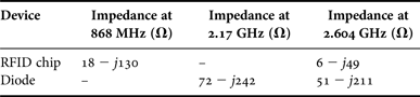
Figure 3 shows the measured impedance for both the RFID chip at 868 MHz and for the Schottky diode at 2.604 GHz, in function of a power sweep from −20 to 0 dBm. The RFID chip impedance is more sensitive to power changes than the diode impedance. For the proof of concept, given the nonlinear variations of the impedance in function of the input power, the impedance values for the step 2 are considered at −10 dBm input power in order to prioritize the activation power of the chip and ensure the RFID communication. This first assumption allows proposing equivalent circuits that could be optimized by simulation in order to ensure the cohabitation of the two rectifiers operating each one at a given input power. Furthermore for the RFID chip, this value of input power is kept constant during the optimization procedure. All measured impedances for both RFID chip and rectifier diode at −10 dBm input power are summarized in Table 1 (note that the chip impedance given in the datasheet at 868 MHz is 23 − j145 Ω).
Measured impedance in function of a power sweep from −20 to 0 dBm for: (a) the RFID chip at 868 MHz and (b) the rectifier diode at 2.604 GHz.
Measured impedances of RFID chip and diode at −10 dBm input power.

Because MOSFET transistors are integrable in CMOS fabrication process, it is worth noting that rectifier circuits could be designed in CMOS technology, using MOSFET transistors connected in diode configuration However, given the modular integration followed in the proposed study (antenna, RFID chip, diodes, etc.) the use of rectifier circuits in CMOS is out of the scope of the paper.
B) Electrical modeling of nonlinear devices
1) Rectifying diode model
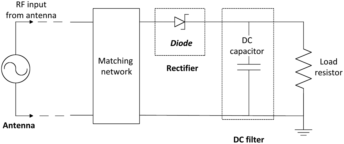
The architecture of the EEH section is shown in Fig. 4. It consists of a single Schottky diode which rectifies the RF input and a capacitor that continuously charges and discharges producing at its output a dc signal feeding a load resistor. The capacitor also filters the RF components that may impairs the dc output and degrades the conversion efficiency of the diode. In order to consider the nonlinear behavior of the diode, its Spice model is used. The HSMS 2860 diode presents the following electrical parameters: low series resistance R s = 6 Ω; zero-bias junction capacitance C jo = 0.18 pF; breakdown voltage threshold V br = 7 V; detection sensitivity of 35 mV/uW [27]. The proposed electrical model does not consider the package parasitic effects, but ensures a rectifier circuit with similar conversion efficiency than a real sample including nonlinear features (i.e. impedance-power dependency and harmonics generation [Reference Ladan, Ghassemi, Ghiotto and Wu32]).
EHH section of the RFID-TR.
2) RFID chip model
An RFID tag architecture is shown in Fig. 5 highlighting the rectenna section. It consists of an antenna, a matching network and a rectifier circuit based on a Dickson topology with two or more diode-based voltage doubler stages [Reference De Vita and Iannaccone33]. The rectifier circuit, responsible of the nonlinear behavior of the RFID chip, determines the RFID chip sensitivity, the capacitive nature of the RFID chip impedance and the harmonic production with specific predominance of odd or even harmonics depending on the chosen rectifying architecture [Reference De Vita and Iannaccone33].
Functional architecture of a passive RFID tag.
From the measured impedances (Fig. 3) it can be concluded that the chip is the most critical parameter regarding the impedance-power dependency, hence the importance of prioritizing the measured values at −10 dBm as reference to build the RFID chip model. Therefore a diode-based RFID chip model is simulated with the aim to produce a similar impedance and harmonic generation to the one characterized at −10 dBm. The variable parameters are the number of diode-based voltage multiplier, the capacitors values, and the resistor at the input.
The proposed equivalent circuit results in a three-stage voltage multiplier using HSMS 2860 Schottky diodes, with coupling capacitors (Cc) and ended in a dc load resistance (Load) as shown in Fig. 6. Additionally, a tuneable shunt resistor (Rin) and a tuneable shunt capacitance (Cin) are set at the input in order to tune small impedance variations due to the package. The design parameters for the RFID chip model are: Cc = 4.3 nF; Cin = 0.146 pF; Rin = 965 Ω; Load = 10 kΩ. The circuit model takes into account the harmonic generation and presents an input impedance close to the one measured for the RFID chip (18 − j130 Ω).
RFID chip equivalent circuit with three voltage-doubler stages based on Dickson topology.
Finally, Fig. 7 compares the measured and modeled impedances for the RFID chip and Schottky diode for an input power at −10 dBm. As expected, the best fitting for the RFID chip is observed around 868 MHz. The proposed models are also found valid for the other frequencies points (notably at 2.17 and 2.604 GHz). With these nonlinear models, a common antenna is designed in the next section.
Measured and modeled impedances for the RFID chip and the Schottky diode at −10 dBm.
Under the assumption of having an optimal commercial RFID chip which activates at −10 dBm, the proposed equivalent model is not evaluated in terms of its RF-to-dc conversion efficiency, but in terms of its impedance and harmonic production supported by experimental measurement. To consider the harvesting performance of the model, some changes may be considered in the architecture by reducing to the minimum the losses (e.g. removing the input resistor) and properly tuning the capacitor values.
C) Single feed dual-band antenna design
Considering the dual-band operation requirements, the chosen antenna topology is inspired from [Reference Liu34] where a modified L–F inverted antenna is presented. The antenna structure allows the use of a ground plane for the rectifier circuitry and a radiator for the RFID communication and rectenna functions, all in a common one side. Using RFID antenna design techniques such as inductive loops to cancel the capacitive impedance of RFID chips and meandering size reduction [Reference Marrocco35, Reference Nguyen, Le, Pham, Nguyen, Dang and Tedjini36], the single-feed dual-band antenna is designed and shown in Fig. 8. Two loops in the ground plane allow the inductive impedance matching to compensate the capacitive effect of devices connected at the antenna input (i.e. the RFID chip and the EEH circuit). Rogers RO4003 substrate with 3.55 permittivity, 0.003 loss tangent and 0.8 mm thickness is used for the prototype. The electromagnetic simulation is performed from DC to 10 GHz in order to cover the first fifth harmonics of the 868 MHz for the RFID section and the fourth harmonics of 2.17 GHz for the EEH section. Pads in where lumped components are soldered are also considered in the electromagnetic simulation. The antenna design procedure is driven by optimization processes (using CST). The optimization goals are: minimum reflection coefficient and maximum gain at both 868 MHz and 2.17 GHz frequencies. The initial design considers the capacitive impedance of the RFID chip as antenna load all along the frequencies of interests in order to mainly define the resonant elements (modified “L” inverted and modified “F” inverted) and the inductive matching (with the loops in the ground).
Structure of the single-feed dual-band antenna. The arrows indicate the pads (i.e. ports) where the lumped elements of the EEH section are connected. The pads are considered in the electromagnetic simulation.
D) Co-simulation design of the RFID-TR system
The integration of the nonlinear circuits and the antenna is simulated in an electric-electromagnetic cooperation environment. The aim of the co-simulation is to optimize the antenna structure and the lumped element values, taking into consideration the nonlinear behavior of RFID and EHH sections. A co-simulation project is defined: (i) for the electromagnetic part the Time Domain Solver is used in Microwave Studio, and (2) for the circuit part “S-parameters” and “Spectral Lines” tasks from Design Studio are used. The co-simulation methodology is performed by two stages.
• The first stage aims to build the impedance matching networks considering the measured S-parameters of the diode and RFID chip and combining the electric and electromagnetic simulation tools. The simulation considers as optimization variables both the antenna structure (mainly the dimensions of inductive loops) and the lumped components values (complementary lumped matching network at 2.17 GHz). The optimization goals are to minimize the reflection coefficient at 868 MHz and 2.17 GHz at the antenna input considering the components connected. At this stage, the simulation does not consider the nonlinear models.
• The second optimization stage considers the lumped components as variables, and takes into account the equivalent nonlinear models of diode and RFID chip [Reference Andia Vera, Nawale, Duroc and Tedjini37]. The optimization goal is to maximize the dc output of the EEH section. An input power of −10 dBm into the RFID chip and the rectifier diode is always considered at 868 MHz and at 2.17 GHz, respectively. It is worth noting that the impedance modulation of the RFID chip produces small variations of the impedance seen by the antenna at the upper frequencies. However, it was experimentally demonstrated that the modulation index performed by the chip decreases as the frequency increases [Reference Andia Vera, Duroc and Tedjini20]. Therefore, although the small variations are not considered in the simulation procedure, the impedance modulation will not produce considerable mismatching with the antenna matched to only one impedance state.
Regarding the dc section, a 3 kΩ load resistance represents the measured impedance of the BAP pin of the chip. Figure 9 presents the block diagram of the second co-simulation stage integrating all the sections of the proposed RFID-TR system. An ideal directional coupler is used to integrate the S-parameters of the antenna with the RFID chip model and an AC source. The co-simulation provides an optimized lumped impedance matching network at 2.17 GHz composed by a 0.2 pF series capacitor and a 6.8 nH shunt inductor.
Electric-electromagnetic co-simulation of the proposed RFID-TR: (a) nonlinear model of the RFID chip and (b) co-simulation integration of the RFID-TR.
The main difference of the proposed co-simulation method with respect to Class-E or Class-F rectifier methods is that the impedance presented at the rectifier is not independently controlled at each frequency but globally controlled by the two optimized matching networks (the distributed network at 868 MHz and the lumped one at 2.17 GHz) thanks to the spectral analysis at the section input (i.e. by maximizing the power transfer at the different RF frequencies) and EEH output (i.e. by minimizing the PSD of RF frequencies and maximizing the dc component). The final goal is to maximize the conversion efficiency of the EEH section. This operation allows the EEH section to cohabit and profit from the RFID section considering that the operation power levels may be different for each section. It is also worth noting that the multi-device waveform effect is not simulated but experimentally proven, therefore the benefit of the effect is not estimated in a priori analysis
1) Prototyping
Finally the realized RFID-TR is shown in Fig. 10. The RFID chip and lumped components are soldered at the pads. A wire is used to inject the harvested dc power into the BAP input of the chip. One notices that the prototyping method (i.e. soldering and components orientation) could impair the performance of the devices and produce deviation from expected results. Actually the extra wire connected into the BAP pin of the RFID chip could add some inductance and impairs the expected operation.
Prototype of the RFID-TR: (a) dual-band antenna, (b) EEH section, (c) EM4325 RFID chip, and (d) connection for harvested dc power. The arrows’ numbers indicate the ports where the lumped elements are soldered.
The performance of the RFID-TR will be evaluated at the frequencies of interest (868 MHz and 2.604 GHz) and under the standard RFID power regulations in Europe, i.e. 35.15 dBm effective isotropic radiated power (EIRP).
IV EXPERIMENTAL RESULTS
A) Measurement setup
To evaluate the performance of the RFID-TR, the measurement procedure has two goals: (i) to measure the dc output across the load resistor in the EEH section (Section IV.B), and (ii) to evaluate the RFID tag performance of the RFID-TR in terms of read range (Section IV.C). The measurement setup shown in Fig. 11 is performed in the anechoic chamber and it is composed by:
• an Agilent N5182A signal generator, which produces a CW at 2.17 GHz, associated with a 7 dB gain horn antenna used for the transmission;
• an Impinj Speedway R420 Revolution RFID reader operating at 868 MHz, associated with a circularly polarized 6 dB gain antenna is used;
• a dc voltmeter connected at the load resistor in order to measure the harvested dc voltage;
• a computer in order to control the equipment for data acquisition and processing.
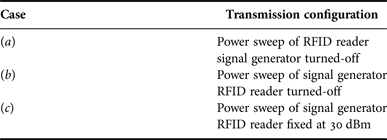
The setup calibration considers the antenna gains, free space propagation losses, and cable losses. Given the multi-source operation (with the RFID reader at 868 MHz and the signal generator at 2.17 GHz), three different transmission configurations are considered in order to better evaluate the operation of the RFID-TR. Table 2 presents the three considered cases.
Measurement setup for the performance evaluation of the RFID-TR.
Transmission configurations for the RFID-TR evaluation.
B) EEH evaluation
Experiments when the RFID reader transmits the maximum allowed power 30 dBm, and the external source is turned-off, i.e. in the case (a), a weak 5 mV dc is measured at the BAP pin. Actually even if the EEH section is optimized at 2.17 GHz, the second and third harmonics of 868 MHz are being rectified in case (a). Figure 12 shows the rectified dc voltage measured at the BAP pin in function of the received input power at 2.17 GHz for cases (b) and (c), calculated using Friis formula under the setup shown in Fig. 11. When the reader is turned-off (case (b)), the dc voltage rises with the input power at 2.17 GHz. Finally the case (c) clearly shows the mutual benefit due to a joint operation of RFID chip and a rectifying circuit.
Rectified dc output voltage in function of the input power at 2.17 GHz for cases (b) and (c) presented in Table 2.
To quantify the effect of the multi-source operation, a power gain figure (G P) is defined in (1) [Reference Boaventura and Carvalho21]. The factor G P defines the power gain obtained in case (c) regarding to the power gain obtained in case (b). Since the dc load resistance is in both cases the same, the dc power can be defined as function of the dc voltages V b and V c, for the cases (b) and (c) respectively. It is worth noting that, contrary to [Reference Boaventura and Carvalho21] in where a similar input power is considered in the comparison, the factor G P defined in this paper includes the gain due to the additional input power supplied by the RFID reader in case (c).
 $${G_P} = 10\mathop {\log} \nolimits_{10} \left( {\displaystyle{{V_c^2} \over {V_b^2}}} \right).$$
Figure 13 shows the calculated G P. A greater cooperation effect can be observed at low-input power, i.e. between −11.3 and −7 dBm. The results are in agreement with the design stage in what concern the optimized operation about −10 dBm. A G P 33 dB higher is obtained when the RFID-TR operates under multi-source configuration compared with the case operating only with the signal generator.
Power gain as function of input power.
C) Read range evaluation
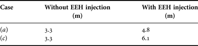
The RFID tag performance of the RFID-TR is evaluated by calculating its read range [Reference Rao, Nikitin and Lam38] using a Speedway Revolution RFID reader [39] for the two cases (a) and (c). Figure 14 shows the read range variations with respect to the Reader Equivalent Isotropically Radiated Power (R EIRP) and compares the results with the scenario without EEH injection. Table 3 summarizes the read range results at 868 MHz.
Read range for the RFID-TR.
Maximum read range without and with EEH injection.
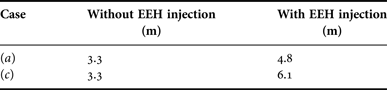
The EEH injection in case (c) allows one to read the RFID-TR at lower R EIRP (i.e. 24 dBm and approximately 2 m read range). Furthermore, when the RFID-TR without EEH injection is read at 35 dBm R EIRP for instance, its maximum read range is 3.3 m, while with EEH injection the read range is 1.5 m higher for case (a) and 2.8 m higher for case (c). The read range enhancement is produced by a different behavior in each case. In case (a), even if the EEH section is tuned at 2.17 GHz, the modulated harmonics produced by the RFID chip are harvested producing the 1.5 m read range enhancement. In case (c), the improvement is due to the harvesting operation at 2.17 GHz but also because there of the combined effect of both RF sources producing a signal with higher PAPR.
V. CONCLUSION
This paper proposes an original design of an RFID tag that embeds an additional rectifier circuit in order to efficiently produce complementary dc power benefiting from multi-source operation and nonlinear effects in the RFID chip. The proposed solution, so-called RFID-TR, is realized and tested via a prototype that integrates an RFID chip operating at 868 MHz, an EEH circuit operating at 2.17 GHz and a common single-feed antenna. The design methodology describes each design step and the procedure to integrate the RFID chip with the external EEH circuit using the common dual band antenna. The experimental results show the enhancement of the harvesting efficiency of the EEH circuit, and also the possible enhancement of the read range when the dc power is injected in the tag itself. The beneficial effect introduced by the double rectifier and multi-source operation is based on the exploitation of the nonlinearities of each rectifier. The proposed design exploits the harmonic generation of the RFID chip and considers the impedance-power dependency of each rectifier in the integration procedure. Additionally, a time-varying envelope signal is obtained by the combination of the modulated reflected chip harmonic and the external RF CW improving the harvesting efficiency.
The paper presents the first findings on the topic with the objective to demonstrate the proposed concept. Some additional efforts could be dedicated to the improvement of the integration technique of RFID and EEH sections by means of more accurate equivalent models of the diode and RFID chip, for instance: (i) in order to better exploit the HB tool and improve the device models, the experimental characterization of the devices used as inputs for the model should consider more harmonic frequencies; (ii) the use of CMOS diode-connected transistors to model the RFID chip rectifier could better reflect the RF operation occurring in the RFID chips.
Some future research paths could be addressed in the use of specific tuned frequencies for the RFID-TR, considering bands with great power density like broadcasting communication systems or frequencies belonging to the Industrial Scientific Medical (ISM) band. Further research efforts could be also dedicated to the combination of design methods such as the used in Class-E or Class-F rectifiers with the proposed composite rectifier method.
ACKNOWLEDGEMENTS
The authors wish to thank Professor Ramon Villarino from Universitat Rovira i Virgili, Tarragona, Spain for his support in the antenna fabrication. A special thanks to the reviewers for their anonymous, voluntary and extensive assessment of our manuscript, thanks for their valuable comments and suggestions that help to improve it.
Gianfranco Andia-Vera He was born in Puno, Peru, in 1986. He received the dual M.Sc. degree in telecommunications engineering from the Universitat Politecnica de Catalunya (UPC), Barcelona, Spain, and the Pontificia Universidad Catolica del Peru (PUCP), Lima, Peru, in 2009, the Postgraduate degree in development and management of networks on information technology from UPC, in 2010, and the Ph.D. degree in optics and radiofrequency from the Grenoble Institute of Technology (Grenoble INP), Valence, France, in 2014. He was a Communication Engineer involved in RF planning and network deployment for a telecom carrier from 2009 to 2011. From 2011 to 2015 he has been with the Laboratoire de Conception et d'Integration des Systemes. His current research interests include RFID, antennas, energy harvesting, wireless networks, and microwave devices. Since 2016 he is RF Engineer in Primo1D and contributes to the development of textil-based RFID applications. He serves as an expert-reviewer for international scientific committees, including IEEE (MTT, MWCL, and Sensors), IET (AP), Cambridge (WPT, IJMWT).
 Shankar Nawale was born on September 25, 1977 in India and received B.E. degree from Dr. B. A. M. University, Aurangabad, (MS), India in 2000, M. Tech. in Electronics and Telecommunication Engineering and Ph.D. in Electronics Engineering from Veermata Jijabai Technological Institute (VJTI), University of Mumbai, (MS), India in 2008 and 2013, respectively. Currently, he is an Associate Professor at Sinhgad Institute of Technology, Lonavala, Pune, MS, and was Head of the Department, Electronics and Telecommunication Engineering since July 2007, where he has taught the subjects such as Electromagnetics, Wave Theory, Antennas, and Microwave Engineering. He is currently working on Energy Harvesting in passive RFID applications.
Yvan Duroc received the Teaching degree Agregation (French national degree) in Applied Physics in 1995 from Ministry of National Education, Higher Education, and Research, France, the Ph.D. degree in Electrical Engineering from the Grenoble Institute of Technology in 2007 and the HDR degree (Habilitation Diriger des Recherches) from the Grenoble University in 2012. He was a Teaching Associate at Esisar Engineering School from 1997 to 2009, where he was an Associate Professor from 2009 to 2013. He is currently a Professor at the University Claude Bernard Lyon 1, France. He is in charge of lectures in signal and image processing, RF and microwave, electronics, and embedded systems for the engineer and M.Sc. levels. His current research interests include microwave and applied signal processing with special attention to ultra-wideband and radio frequency identification technologies, backscattered modulations, energy harvesting, sensors, and antennas. He is the member of several TPC and serves as an expert-reviewer for national and international scientific committees and conferences, including IEEE, IET, Cambridge, PIER, Hindawi, Eurasip, URSI, EUCAP, ATC, ANR, and ARC6. Professor Duroc is the Vice-chair of the URSI Commission C, France.
Smail Tedjini received Doctor of Physics degree from Grenoble University in 1985, and became a full Professor in 1993. Main topics are Electromagnetism, RF, Wireless and Optoelectronics. Current research concerns wireless systems in particular RFID. He is the founder and past Director of LCIS Laboratory and actually, he was former ORSYS group leader. He supervised more than 30 Ph.D. scholars and has more than 300 publications. He served as an Examiner/reviewer for tens of Ph.D. for various universities (France, Germany, Italy, Vietnam, Australia, Singapore, India, Brazil, Maghreb, etc.). He is Member of several TPC and serves as expert for international scientific committees and conferences, including ISO, Piers, IEEE, URSI, and EuCap. He organized several conferences/workshops. He was the Past President and founder of the IEEE-CPMT French Chapter, Vice-President of IEEE France Section, and Chair of URSI Commission “D” 2011–2014. Recently, he was elected as the President of URSI – France 2015–2018.