I. INTRODUCTION
Bulk SiC is a wide-gap semiconductor and it manifests in many forms.Reference Lindefelt1 There are more than 200 known polytypes of SiC. These polytypes are attributed to different stacking sequences of Si and C atoms in different bilayers. Depending on its polytype, its energy gap ranges from 2.4 to 3.3 eV. Besides large energy gaps, SiC also exhibits a large thermal conductivity (three times that of silicon) and a high breakdown voltage (five times that of silicon) that make it a suitable material for high-power electronic devices and high frequency transistors.Reference van Haeringen, Bobbert and Backes2, Reference Matos3 The large energy gaps of SiC have been exploited in the fabrication of blue light-emitting diodes or blue laser diodes. These interesting properties of bulk SiC have prompted us to pose the question how they would manifest themselves in nanostructured systems. Therefore, in this work, we have carried out a systematic theoretical study of SiC-based nanowires (NWs) to ascertain how the quasi-one-dimensional characteristics of NWs affect the properties of the bulk SiC and whether the resulting properties could lead to interesting and useful device applications.
The synthesis of large quantities of well-oriented crystalline 3C–SiC NWs along <111> and <100> orientations,Reference Sun, Li, Wong, Wong, Lee, Lee and Teo4–Reference Zhang, Han, Zheng, Zhang, Zhang, Fu, Ji, Hao, Guo and Wang18 as well as that of 2H–SiC NWs along the <0001> direction with an intergrowth of 3C–SiC structure along <111> direction,Reference Zhou, Sun, Muñoz, Dalton, Collin, Wang, Zakhidov and Baughman19 have been reported in the literature. According to the reported experiments, the yield of SiC NWs is substantially greater than that of SiC whiskers and bulk SiC.Reference Zhou, Yang, Yang, Zhu, Yan and Zhang15, Reference Nhuapeng, Thamjaree, Kumfu, Singjai and Tunkasiri20, Reference Han, Zhang, Zheng, Zhang, Zhang, Hao, Guo, Yuan and Wang21 Some SiC NWs have been shown to exhibit high electron field emission with high stability.Reference Zhou, Liu and Zhang6, Reference Pan, Lai, Au, Duan, Zhou, Shi, Wang, Lee, Wong, Lee and Xie13, Reference Niu, Wang and Xu22 A strong broad photoluminescence peak around 450 nm has also been reported for 3C–SiC nanocrystallites.Reference Hu, Lu, Tang, Deng, Jiang, Qian, Yu, Zhou, Liu and Wu9 These experimental results have definitely given credence to the notion that SiC NWs could be used as building blocks for electronic and optoelectronic devices. However, without a detailed and systematic theoretical study of the structural and electronic properties of SiC NWs, the scope of the applications would be limited due to the lack of a fundamental understanding of how the properties of SiC-based NWs depend on their structures, morphologies, diameters, and orientations. It should be noted that there are some theoretical studies reported in the literature on mechanical properties of 3C–SiC along <111> direction using Tersoff potentialReference Kim, Han and Lee23, Reference Makeev, Srivastava and Menon24 and on the electronic and structural properties of 3C–SiC NWs of very small diameters along <001> direction using density functional theory (DFT).Reference Rurali25
In this work, we have conducted a comprehensive study of interplay among morphology, orientation, and size on the relative stability and the electronic characteristics of four plausible polytypes of SiC NWs, using the DFT-based simulation [i.e., the Vienna ab initio simulation package (VASP)Reference Kresse and Hafner26–Reference Kresse28] as well as a semiempirical Hamiltonian-based simulation.Reference Leahy, Yu, Jayanthi and Wu29–Reference Yu, Wu and Jayanthi31 We chose to study 3C–, 2H–, 4H–, and 6H–SiC NWs because their corresponding bulk counterparts are the most common polytypes of the bulk SiC. The initial structures of these four polytypes of SiC NWs were obtained by truncating the bulk 3C–, 2H–, 4H–, and 6H–SiC along different directions and considering different shapes for the cross-sectional morphologies. Specifically, we studied SiC NWs oriented along <111>, <001>, <011>, and <0001> directions and considered the following cross-sectional morphologies: hexagons, polygons, rhombuses, squares, circles, octagons, and triangles. Our emphasis in this work is on how the size, the shape, and the orientation of the SiC NW influence the energetics (i.e., relative stabilities) and the electronic characteristics [i.e., electronic density of states (EDOS)] of NWs. For example, we have found that the <0001>-oriented hexagonal 2H–SiC NWs are the most stable (in energy) among all SiC NWs studied and yet maintain their semiconducting nature even when their diameter approaches 1 nm. While other SiC NWs, regardless of their morphology and orientation, possess substantial impurity states in the vicinity of the Fermi level for smaller diameters (∼1.5 nm).
II. METHODOLOGY AND CALCULATIONS
In this work, we have used a first-principles method for studying SiC NWs with diameters less than 3.5 nm and a semiempirical method for studying larger diameter NWs up to 14 nm. The first-principles method based on DFT and as implemented in the VASPReference Kresse and Hafner26–Reference Kresse28 was used in our calculation. The DFT calculation is performed using the generalized gradient approximation. The electron–ion interactions are described by Vanderbilt’s ultrasoft pseudopotential,Reference Vanderbilt32–Reference Laasonen, Pasquarello, Car, Lee and Vanderbilt34 and exchange correlations of Perdew and Wang (PW91)Reference Wang and Perdew35 were used. In determining optimized structures of all the different systems considered in this work (namely, NWs of different polytypes, morphology, orientation, and diameters), we applied the one-dimensional periodic boundary condition to the systems along the wire axis with a vacuum region (∼15 Å) between wires to ensure that there were no interactions between wires. Several k points were taken along the wire axis according to the Monkhorst–Pack schemeReference Monkhorst and Pack36 so as to ensure the convergence of the total energy. For the total energy calculation, the cutoff energy for the plane wave basis set was taken to be 300 eV, and the energy convergence for the self-consistent calculation was set to 10−4 eV. The structures for all cases were relaxed using a conjugate gradient algorithm until the atomic force was less than 10−3 eV/Å. Corresponding to this force convergence, the calculated total energy per atom for all relaxed structures converged to an accuracy of 10−6 eV per atom.
In our semiempirical calculations, we have used highly efficient and reliable quantum mechanical method based on a recently developed self-consistent and environment-dependent (SCED) HamiltonianReference Leahy, Yu, Jayanthi and Wu29–Reference Yu, Wu and Jayanthi31 implemented in the framework of linear combination of atomic orbitals (LCAO) (see the Appendix for the brief description of the SCED-LCAO Hamiltonian and its reliability and efficiency). The calculations are conducted in the real space. The lattice vector along the NW axis is set to be sufficiently large to ensure that the inclusion of all interactions among atoms consistent with the SCED-LCAO Hamiltonian. For SiC NWs with its diameter larger than 4.5 nm (i.e., system sizes > 1000 atoms), we have used the order-N algorithmReference Jayanthi, Wu, Cocks, Luo, Xie, Menon and Yang37, Reference Wu and Jayanthi38 for the molecular dynamics scheme based on the SCED-LCAO Hamiltonian. The structures for all cases were fully relaxed until the total energy is converged to 10−4 eV/atom as well as the atomic force was less than 10−3 eV/Å.
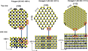
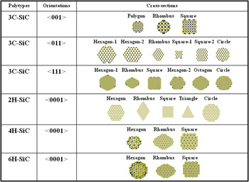
To systematically study the energetic and morphologic aspects of the SiC NWs, we have generated several initial configurations of SiC NWs with different morphologies and orientations. The configurations considered in this work include the following cross-sectional truncations: (i) bulk 3C–SiC along <001>, <011>, and <111> orientations, (ii) bulk 2H–SiC along the <0001> orientation, (iii) bulk 4H–SiC along the <0001> orientation, and (iv) bulk 6H–SiC along the <0001> orientation, respectively. To ensure that the SiC NWs considered in this work maintain the compositional symmetry of the chemical species, we generated them by cleaving the bulk in such a way that the wire axis passes through the interstitial region of the bulk lattice. The energetics and stability of the SiC NWs are, therefore, expected to depend on factors such as orientations, morphologies, and diameters. Based on this consideration, we constructed several different cross-sectional shapes for each given polytype of SiC NWs. The rationale behind the design of NWs with different shapes for a given orientation and diameter is to determine which shape is best suited for lowering the surface energy of the NW upon relaxation. In other words, which NW shape can reduce the number of dangling bonds on its surface by the formation of dimers, leading to an energetically favorable structure? With this in mind, we have designed initial structures of SiC NWs of different shapes for each orientation such that there is no more than one dangling bond on their surfaces. This leads to different possible C–C or Si–Si dimer arrangements on the NW surface. Therefore, in addition to the major Si–C bonds on the NW surface, there are also C–C and Si–Si bonds with the ratio of the number of the C–C bonds to the Si–Si bonds being 1:1. It should be noted that the formation of different arrangements C–C and Si–Si dimer rows on the NW surface depends on the NW orientation and its morphology with the purpose of reducing the number of dangling bonds on NW surfaces. The bare NW surface of SiC constructed in this way is less reactive than the NW surface with more than two dangling bonds on the surface atoms. In the case of <001>-oriented 3C–SiC NWs, such plausible shapes will be formed mainly by {100} and {110} facets and the associated cross sections will be the polygon, the rhombus, and the square, respectively. It can be seen from the leftmost image in Fig. 1 that for polygon-shaped wires, the dimers are formed at the junction of {100} and {110} facets (top left) with the C–C/Si–Si dimer rows parallel to the wire axis (bottom left). In the case of <011>-oriented 3C–SiC NWs, the plausible shapes having low surface energy will be formed mainly by {100}, {110}, and {111} facets. The associated cross sections will be the hexagons with the dimers on the surface either perpendicular (referred as Hexagon-1, see the center image in Fig. 1) or parallel (referred as Hexagon-2) to the NW axis, or the rhombus, or the squares with the dimers on the surface either perpendicular (referred as Square-1) or parallel (referred as Square-2) to the NW axis, or the circle, respectively. In the case of <111>-oriented 3C–SiC NWs, the plausible shapes will be formed mainly by {110} facets. To eliminate the atoms with more than one dangling bonds, the {112} facets were also introduced. Therefore, the possible initial cross sections will be the hexagons with the dimers on the surface either at the corners of the hexagons (referred as Hexagon-1, see the rightmost image in Fig. 1) or on the edges of the hexagons (referred as Hexagon-2), or the rhombus, or the square, or the octagon, or the circle, respectively. A summary of all types of morphologies considered in this work including other orientations and polytypes (e.g., <0001>-oriented 2H–SiC NWs, <0001>-oriented 4H–SiC NWs, and <0001>-oriented 6H–SiC NWs) are summarized in Fig. 2. For SiC NWs considered in this work, the diameter d was defined from the relation  $N = {\rm{\rho }}d^2 {\rm{\pi }}L/4$, where N is the number of atoms in the volume of the unit cell (
 $d^2 {\rm{\pi }}L/4$), L the length of the unit cell along the NW axis, and ρ the density of the bulk 3C–SiC.
Cross-sectional and side morphologies, respectively, of 3C–SiC NWs cut along <001> (left), <011> (middle), and <111> (right) directions. Orientations and locations of dimers are different in each of these cases, where C–C dimers (Si–Si dimers) are indicated by black (yellow) balls and sticks. In the case of <011>-oriented NWs with hexagonal morphology (Hexagon-1), the dimers are oriented perpendicular to the NW axis and this is more apparent in the side view; in the case of <111>-oriented NWs with hexagonal morphology, the dimers are located at the corners of the hexagon. A circular loop (red) enclosing the dimers is drawn to indicate the location of dimers in each of these cases. The vertical arrows in each wire in the side view denote the orientation of the wire axis.

Different polytypes, orientations, and shapes of SiC NWs considered in this work. The shapes correspond to different types of cross-sectional morphologies of NWs. In the case of <011>-oriented 3C–SiC NWs, Hexagon-1 (Square-1) and Hexagon-2 (Square-2) refer to hexagon-shaped (square-shaped) cross-sectional morphologies with dimers perpendicular and parallel to the NW axis, respectively. On the other hand, for <111>-oriented 3C–SiC NWs, Hexagon-1 and Hexagon-2 refer to hexagon-shaped cross-sectional morphologies with dimers on the corners and on the edges of the hexagons, respectively. The yellow balls represent Si atoms and the black balls represent carbon atoms.

III. ENERGETICS OF SIC NW: INTERPLAY OF MORPHOLOGY, ORIENTATION, AND SIZE
To gain an understanding of relative stabilities of SiC NWs of different polytypes, morphologies, orientations, and diameters, we have performed structural relaxations of these systems using either the DFT method (VASP package)Reference Kresse and Hafner26–Reference Kresse28 or the SCED-LCAO methodReference Leahy, Yu, Jayanthi and Wu29–Reference Yu, Wu and Jayanthi31 and calculated their corresponding total energies per atom. The DFT method has been used for wires with 1 nm < d < 3.5 nm diameters, while latter method is used for larger diameter wires up to 14 nm.
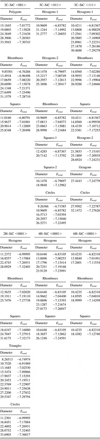
The results for the total energy per atom (E total) as a function of the NW’s diameter are shown for all the systems studied in this work in Fig. 3. Since energy differences between some structures are not easy to decipher from the plots, we have tabulated the total energies per atom corresponding to each of these structures in Table I. It should be noted that when the diameter is very small, one cannot distinguish the shape differences between different morphologies (e.g., Hexagon-1/Rhombus and Hexagon-2/Square-2 in 3C–SiC <011> NWs, Hexagon-1/Square in 3C–SiC <111> NWs, etc.). This is also true for small diameter NWs of other polytypes.
The total energy per atom (E total) versus the diameter of SiC NWs corresponding to different orientations and morphologies: <001>-oriented 3C–SiC NWs (upper left), <011>-oriented 3C–SiC NWs (upper middle), <111>-oriented 3C–SiC NWs (upper right), <0001>-oriented 2H–SiC NWs (bottom left), <0001>-oriented 4H–SiC NWs (bottom middle), and <0001>-oriented 6H–SiC NWs (bottom right). The notations used to represent different morphologies are provided in the Fig. 2.

The calculated total energy per atom E total (eV/atom) is given as a function of its diameter (Å) for several types of SiC NWs: 3C–SiC, 2H–SiC, and 6H–SiC NWs of different morphologies and orientations. The convergence in the value of the total energy per atom was achieved to a tolerance of approximately 10−6 eV/atom.

It can be seen from Fig. 3 that for all the systems considered, total energies per atom (E total) decrease monotonically with increasing diameters of NWs and they are expected to reach their corresponding bulk values (of the polytype) when the diameter approaches infinity. This is because smaller diameter NWs experience larger strains due to enhanced surface effects caused by larger ratios of surface/core atoms. Therefore, the total energy/atom of smaller diameter NWs are higher compared to larger diameter NWs. In the case of <001>-oriented 3C–SiC NWs [Fig. 3 (upper left)], wires with polygonal- and rhombus-shaped morphologies are energetically more stable than NWs with other morphologies. In particular, for NWs with square morphologies, the atoms on the corners of the square surface are unstable (e.g., E total is ∼20 meV higher than those of polygon-shaped NWs and rhombus-shaped ones for diameters larger than 2.4 nm). In the case of <011>-oriented 3C–SiC NWs [Fig. 3 (upper middle)], E total differences for different morphologies are quite similar when the diameter is smaller than 2 nm. But when the diameter increases beyond 2 nm, the wires with rhombus-shaped morphologies are energetically unstable compared to wires with other morphologies (e.g., NWs with circular and the hexagonal morphologies are ∼10 meV/atom lower in energy compared to NWs with rhombus-shaped cross section for diameters larger than 2.5 nm). Finally, in the case of <111>-oriented 3C–SiC NWs, Hexagon-1 wires with the dimers on the surface at the corners of the hexagon are energetically more stable than NWs with other morphologies with increasing diameter [Fig. 3 (upper right)]. Comparing the total energies of 3C–SiC NWs along <001>, <011>, and <111> [see Fig. 3 (upper panel): left, middle, and right], it is found that wires oriented along <001> and <111> directions are more stable than those oriented along the <011> direction. Similarly, in the cases of <0001>-oriented 2H–SiC, the wires with the hexagonal/circle morphologies are energetically more stable than the wires with other morphologies [Fig. 3 (bottom left)]. While, in the cases of <0001>-oriented 4H–SiC and 6H–SiC NWs, the wires with the hexagonal morphology are slightly lower in energy (approximately a few meV/atom for diameters larger than 1.6 nm) than those with rhombus/square morphologies (see Fig. 3 bottom middle and right). The results shown in Fig. 3 and Table I demonstrate that the lesser the extent of the surface reconstruction associated with a given morphology and orientation of the wire, the lower is the corresponding total energy per atom of that system. We would like to remark that within the accuracy of our calculations, for a given polytype and a given orientation, the calculated energy differences for different morphologies are small (<20 meV) and yet distinguishable.
Based on our total energy per atom calculation for different orientations and morphologies, we have calculated the relative energy per atom (i.e., the total energy per atom of a SiC NW relative to that of its bulk counterpart) versus diameter for those energetically favored wires, such as polygonal-shaped wires for 3C–SiC along the <001> direction, hexagonal-shaped wires for 3C–SiC along the <111> direction as well as for 2H–, 4H–, and 6H–SiC along the <0001> direction. In Fig. 4(a), we show the results obtained using the DFT-based VASP for wires of diameters up to 3.5 nm (∼500 atoms in the unit cell). It can be seen that, among the SiC NWs investigated in this work, <0001>-oriented 2H–SiC NWs are energetically more stable compared to 3C–, 4H–, and 6H–SiC NWs. For SiC NWs with diameters larger than 4 nm, we have used an efficient and reliable quantum mechanics simulation scheme based on the SCED-LCAO Hamiltonian.Reference Leahy, Yu, Jayanthi and Wu29–Reference Yu, Wu and Jayanthi31 Using this method, simulations have been performed for SiC NWs with diameters up to 14 nm (∼19,600 atoms in the unit cell). The use of this method is needed to predict the stability of SiC NWs at larger diameters and, in particular, to investigate whether there is any change in the trend of the relative energy versus diameter curve favoring a NW of different morphology/orientation at larger diameters. It is computationally expensive and almost impossible to perform exhaustive calculations as we have done here with different morphologies and orientations for diameters up to 14 nm using only DFT method. Therefore, we have used combinations of DFT and semiempirical approaches to gather as much useful information as possible. It should be pointed out that the reliability of SCED-LCAO approach has been tested extensively for Si-based and C-based systems, and in the present case, we have compared results obtained using SCED-LCAO against DFT for diameters up to 3.5 nm before drawing any conclusion about larger diameter SiC NWs.
The relative energy versus the diameter of SiC NWs corresponding to different orientations and different morphologies (e.g., hexagonal 3C–SiC along the <111> direction, polygonal 3C–SiC along the <001> direction, hexagonal 2H–SiC along the <0001> direction, hexagonal 4H–SiC along the <0001> direction, and hexagonal 6H–SiC along the <0001> direction), calculated using (a) the DFT-based VASP packageReference Kresse and Hafner26–Reference Kresse28 for d up to 3.5 nm and (b) the SCED-LCAO methodReference Leahy, Yu, Jayanthi and Wu29–Reference Yu, Wu and Jayanthi31 for d up to 14 nm, respectively. The relative energy is defined as the difference between the total energy per atom of any configuration of the SiC NW and the total energy per atom of the corresponding bulk counterparts.

The results using the SCED-LCAO method are depicted in Fig. 4(b), where the relative energy versus diameter is shown for a variety of SiC NWs with different orientations and shapes. It can be seen from this figure that the results for the energy ordering of SiC NWs with different shapes and orientations as predicted by the SCED-LCAO method agree with those of the DFT methodReference Kresse and Hafner26–Reference Kresse28 for diameters up to ∼3.5 nm. More importantly, it can be seen that <0001>-oriented 2H–SiC NWs are energetically more stable than 3C–, 4H–, and 6H–SiC NWs in the entire diameter range 1 nm < d < 14 nm.
IV. ELECTRONIC DENSITIES OF STATES
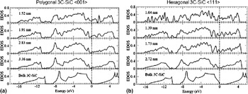
For the energetically stable SiC NWs found in the previous section, we have calculated the EDOS using DFT/VASPReference Kresse and Hafner26–Reference Kresse28 method. More specifically, we have calculated the EDOS of <001>-oriented polygonal 3C–SiC NWs, <111>-oriented hexagonal 3C–SiC NWs, and <0001>-oriented hexagonal 2H–, 4H–, and 6H–SiC NWs for diameters up to ∼3.5 nm. Figures 5(a) and 5(b) show the EDOS of the polygonal 3C–SiC NWs with their wire axes along the <001> direction [Fig. 5(a)] and the EDOS of the hexagonal 3C–SiC NWs with their wire axes along <111> direction [Fig. 5(b)], respectively, for selected diameters. The EDOS of bulk 3C–SiC is also presented at the bottom of each panel. The bulk 3C–SiC is a semiconductor with a calculated energy gap of 1.42 eV. It should be note that the energy gap of bulk 3C–SiC (1.42 eV) calculated using VASPReference Kresse and Hafner26–Reference Kresse28 is smaller compared to the experimental value (2.39 eV) as reported in Ref. Reference Bimburg, Blachnik, Cardona, Dean, Grave, Harbeke, Hüber, Kaufmann, Kress, von Münch, Rössler, Schneider, Schulz, Skolnick, Madelung, Madelung and Landolt-Bürnstein39. On the other hand, the results for 3C–SiC NWs (1 nm < d <3 nm) clearly indicate that there are impurity states near the Fermi level. By comparing the EDOS of 3C–SiC NWs with the EDOS of bulk 3C–SiC, it is clear that such states originate mainly from the surface reconstructions and any remnant dangling bonds on the NW surface. It can also be seen that the smaller the diameter of 3C–SiC NWs, the more impurity states appear near the Fermi level. Since the ratio of surface/core atoms is larger in a smaller diameter wire, participations by surface atoms are more significant leading to robust surface reconstructions. Similar findings were reported by RuraliReference Rurali25 in a DFT calculation of C- and Si-coated 3C–SiC NWs along the <001> direction.
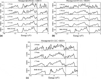
Similarly, hexagonal-shaped 4H–SiC NWs along <0001> and 6H–SiC NWs along <0001> exhibit states near the Fermi level in the EDOS [see Figs. 6(b) and 6(c)] for 1 nm < d < 1.5 nm arising from surface reconstructions that lead to a gapless characteristics for also these systems. In contrast, their bulk counterparts are typically wide-band gap semiconductors with calculated band gaps of 2.28 and 2.07 eV, respectively. For comparison purposes, the bulk EDOS for these systems are also plotted in the above figures. Once again, the energy gaps of bulk 4H–SiC (2.28 eV) and 6H–SiC (2.07 eV) as obtained by DFT (VASP) calculations are underestimated compared to the measured values of 3.26 and 3.02 eV, respectively.Reference Bimburg, Blachnik, Cardona, Dean, Grave, Harbeke, Hüber, Kaufmann, Kress, von Münch, Rössler, Schneider, Schulz, Skolnick, Madelung, Madelung and Landolt-Bürnstein39 It can also be seen from the plots of EDOS versus diameter [see Figs. 5(a) and 5(b) and Figs. 6 (b) and 6(c)] that, as the diameter of the wire increases, the impurity states near the Fermi level of 3C–, 4H–, and 6H–SiC NWs are reduced due to weaker surface reconstructions in larger diameter wires.
Electronic densities of states (EDOS) of (a) polygonal 3C–SiC NWs with <001> orientation and (b) hexagonal 3C–SiC NWs with <111> orientation, respectively using DFT calculations. The numbers in each panel indicate the diameters of the wires. The EDOS of the corresponding bulk counterpart (bulk 3C–SiC) is also plotted at the bottom of each panel for comparison. Note that the energy gap of bulk 3C–SiC (1.42 eV) was underestimated by the DFT calculation (compared to the measured value of 2.39 eVReference Bimburg, Blachnik, Cardona, Dean, Grave, Harbeke, Hüber, Kaufmann, Kress, von Münch, Rössler, Schneider, Schulz, Skolnick, Madelung, Madelung and Landolt-Bürnstein39). The vertical dashed lines are the Fermi levels.

Electronic densities of states (EDOS) of (a) hexagonal 2H–SiC NWs with <0001> orientation, (b) hexagonal 4H–SiC NWs with <0001> orientation, and (c) hexagonal 6H–SiC NWs with <0001> orientation, respectively, using DFT calculations. The numbers in each panel indicate the diameters of the wires. The EDOS of the corresponding bulk counterparts (i.e., bulk 2H–SiC, 4H–SiC, and 6H–SiC) are plotted at the bottom of each panel for comparisons. Note that the energy gaps of bulk 2H–, 4H–, and 6H–SiC (2.38, 2.28, and 2.07 eV) were underestimated by the DFT calculation (compared to the measured values of 3.3, 3.26, and 3.02 eVReference Bimburg, Blachnik, Cardona, Dean, Grave, Harbeke, Hüber, Kaufmann, Kress, von Münch, Rössler, Schneider, Schulz, Skolnick, Madelung, Madelung and Landolt-Bürnstein39). The vertical dashed lines are the Fermi levels.

In the case of hexagonal 2H–SiC NWs oriented along <0001>, one finds that in the EDOS plot, there are no impurity states close to the Fermi level [Fig. 6(a)] for 1 nm < d < 3 nm with clear evidence for energy gaps. This suggests a semiconducting behavior for these systems. It is also seen that the energy gap is ∼1.3 eV when the diameter d is 1.12 nm and it is ∼1.5 eV when d is ∼2.81 nm. The energy gap is expected to approach that of the bulk 2H–SiC (∼2.38 eV) when the diameter approaches infinity. It should be noted that the energy gap of bulk 2H–SiC (2.38 eV) was underestimated by DFT/VASP compared to the measured value of 3.3 eV.Reference Bimburg, Blachnik, Cardona, Dean, Grave, Harbeke, Hüber, Kaufmann, Kress, von Münch, Rössler, Schneider, Schulz, Skolnick, Madelung, Madelung and Landolt-Bürnstein39 Hence, it is expected that the energy gaps of the NWs were also underestimated accordingly. But the qualitative result of the dependence of the gap on the diameter is expected to be correct. These results suggest that the diameter dependence of the energy gap of hexagonal 2H–SiC NWs exhibits a redshift as the diameter is reduced. We have analyzed the surface reconstruction of the hexagonal 2H–SiC NWs and found that these NWs exhibit much weaker surface reconstructions compared to other SiC NWs. This enables them to preserve most of their crystalline structure and therefore remain semiconducting even after these structures are relaxed. On the other hand, the small redshift of the energy gap is an indication of the increasing contribution of the surface reconstruction as the diameter of the 2H–SiC NWs decreases but weaker compared to other SiC NWs.
V. CONCLUSIONS
This work elucidates the role played by the size, shape, and orientation of SiC NWs, designed from the most commonly observed bulk polytypes, on their structure–property relationships, in particular on their stability and electronic characteristics. It is interesting to note that, while bulk SiC is a wide-gap semiconductor, most SiC NWs possess substantial impurity states in the vicinity of Fermi level for diameters less than 1.5 nm except 2H–SiC oriented along <0001> with hexagonal morphology that retains its semiconducting characteristics down to 1 nm. It was also found that 2H–SiC NW oriented along <0001> is the most stable one among the NWs examined in the diameter range 1 nm < d < 14 nm. The energy gaps of 2H–SiC NWs increase with increasing diameters of the wires. The gapless features in EDOS of smaller diameter (∼1.5 nm) SiC NWs of other polytypes are attributed to impurity states arising from the surface reconstructions and any remnant dangling bonds on NW surfaces. It is expected that there will be a crossover where such impurity states near the Fermi level will disappear and a semiconducting behavior will appear at larger diameters. The tuning of electronic properties of SiC NWs according to size, shape, and orientation is expected to have a significant impact on future designs of nanoscale electronic devices.
Finally, we would like to remark on the following: (i) while Mott–Hubbard states have been observed for 6H–SiC (0001) surface,Reference Ramachandran and Feenstra40 currently, there are no theoretical or experimental investigations demonstrating the existence of such states for SiC NWs. Even through the calculated EDOSs for SiC NWs exhibit substantial impurity states in the vicinity of Fermi level for diameters less than 1.5 nm (except 2H–SiC NWs), the DFT method used here is not equipped to ascertain whether a Mott transition would occur for SiC NWs since it is based on a single-particle picture. To settle the issue whether a Mott transition could occur in SiC NWs requires an experimental investigation, (ii) it might be interesting to investigate in a future study the role played by reactive centers or dangling bonds on the surface reconstruction and electronic states when gaseous species are adsorbed on SiC NWs; (iii) by controlling the annealing process in the synthesis of the SiC NWs, it is possible to realize different types of morphologies and surface reconstructions considered in the present work; and (iv) since our calculations are based on zero temperature calculations, it is conceivable that one may obtain different results at elevated temperatures.
ACKNOWLEDGMENTS
We would like to acknowledge the funding support for this work received from various agencies: U.S. DOE (DE-FG02-00ER4582), NSF (DMR-0112824), and KSEF. The computing cycles obtained from the Cardinal Research Cluster at the University of Louisville are also acknowledged. We would like to acknowledge our discussions with Mr. Sanguo Shen.
APPENDIX
A brief description of the SCED-LCAO Hamiltonian is presented in this section. The details of this method can be found elsewhere.Reference Leahy, Yu, Jayanthi and Wu29–Reference Yu, Wu and Jayanthi31 The diagonal and off-diagonal matrix elements of the SCED-LCAO Hamiltonian are given as follows:
 $$H_{i{\rm{\alpha }},i{\rm{\alpha }}}^{{\rm{SCED}} - {\rm{LCAO}}} = {\rm{\varepsilon }}_{{\rm{i\alpha }}} + (N_i - Z_i )U_i + \mathop\sum\limits_{k \ne i} {[N_k V_N (R_{ik} ) - Z_k V_Z (R_{ik} )} ]\quad,$$
 $$ H_{i{\rm{\alpha }},j{\rm{\beta }}}^{{\rm{SCED}} - {\rm{LCAO}}} = {1 \over 2} \{ {({\rm{\varepsilon }}_{i{\rm{\alpha }}}^' + {\rm{\varepsilon }}_{j{\rm{\beta }}}^' )K(R_{ij} ) + [(N_i - Z_i )U_i + (N_j - Z_j )U_j ]} + { [ {\mathop\sum\limits_{k \ne i} {(N_k V_N (R_{ik} ) - Z_k V_Z (R_{ik} ))} + \mathop\sum\limits_{k \ne j} {(N_k V_N (R_{jk} ) - Z_k V_Z (R_{jk} ))} } ]} \}S_{i{\rm{\alpha }},j{\rm{\beta }}}\quad . \cr} $$
The physical significances of parameters and parameterized functions appearing in the above equations have been discussed at length in Ref. Reference Leahy, Yu, Jayanthi and Wu29. For example,  ${\rm{\varepsilon }}_{i{\rm{\alpha }}} $ may be construed as the orbital energy of the α-orbital of the atom at site i,
 $N_i $ the number of electrons associated with the atom at site i,
 $Z_i $ the number of valence electrons at the site i,
 $U_i $ the Hubbard-like energy representing the on-site correlation energy,
 $V_N (R_{ik} )$ the electron–electron energy per number of electrons at site k between an electron distribution at site i and the electron distribution at site k,
 $V_Z (R_{ik} )$ the electron–ion interaction energy between electrons associated with the atom at site i and the ion at site k per number of ionic charge,
 ${\rm{\varepsilon }}_{i{\rm{\alpha }}}^’ $ is an energy related to
 ${\rm{\varepsilon }}_{i{\rm{\alpha }}} $ that reflects the presence of its neighbor j,
 $K(R_{ij} )$ a scaling function, and
 $S_{i{\rm{\alpha }},\,j{\rm{\beta }}} $the overlapping matrix.
We model  $V_Z (R_{ik} )$ by the following parameterized function:
 $V_Z (R_{ik} ) = (E_0 /R_{ik} )\{ 1 - (1 + B_z R_{ik} )e^{ - {\rm{\alpha }}_z R_{ik} } \} $ based on its quantum mechanical origin. We have chosen to represent
 $V_N (R_{ik} )$ in terms of
 $V_Z (R_{ik} )$ using a short-range function
 ${V_N (R_{ik} )\; = V_Z (R_{ik} )\; + \;\Delta V_N (R_{ik} )}$ since both
 $V_N (R_{ik} )$ and
 $V_Z (R_{ik} )$ must approach
 ${E_{0} {/ R_{\,\rm{ik}} } \, = {e^{\rm{2}} /{\rm{4\pi \varepsilon }}_0 R_{ik} }}$ as
 $R_{ik} \to \infty $. The overlap matrix elements
 $S_{i{\rm{\alpha }},\,j{\rm{\beta }}} (R_{ij} )$ are expressed in terms of
 $S_{ij,{\rm{\tau }}} $, with τ denoting molecular orbitals ss σ, sp σ, pp σ, and pp π in a sp 3 configuration. Our careful analysis during the initial construction of the framework of the SCED-LCAO Hamiltonian led us to model these short-range functions (S functions as well as ΔV) by a parametric function of the type
 $(A + B R)(1 + e^{ - {{\rm{\alpha}} d}}} )/(1 + e^{ - {\rm{\alpha }} (d - R)} )$. We found this choice of the function to be flexible. The parameters appearing in the SCED-LCAO Hamiltonian are determined by fitting them to series of structural and electronic properties of both bulk phases and clusters that allow an appropriate representation of the chemistry of the element under consideration.Reference Leahy, Yu, Jayanthi and Wu29
In Eqs. (A1) and (A2),  $N_i $, the number of electrons associated with the atom at site i, is to be determined through iterated solutions to the general eigenvalue equation based on the SCED-LCAO Hamiltonian of the system (
 $Hc^{\rm{\lambda }} = E_{\rm{\lambda }} Sc^{\rm{\lambda }} $, with
 $E_{\rm{\lambda }} $ being the eigenvalue for the eigenvector
 $c^{\rm{\lambda }} $) until
 $N_i = \mathop\sum\limits_{{\rm{\alpha }},{\rm{\lambda }}} {f_{\rm{\lambda }} \left( {c_{i{\rm{\alpha }}}^{\rm{\lambda }} } \right)^2 } + \mathop\sum\limits_{{\rm{\alpha }},j{\rm{\beta }},{\rm{\lambda }}(j \ne i)} {f_{\rm{\lambda }} c_{i{\rm{\alpha }}}^{\rm{\lambda }} c_{j{\rm{\beta }}}^{\rm{\lambda }} S_{j{\rm{\beta }},i{\rm{\alpha }}} } $reaches self-consistency.
The total energy and the l th component of the force acting on an atom at site i of the system are given by Eqs. (A3) and (A4), respectively (see Ref. Reference Leahy, Yu, Jayanthi and Wu29).
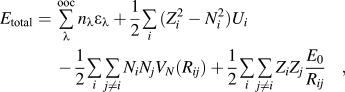 $$E_{{\rm{total}}} =\, \mathop\sum\limits_{\rm{\lambda }}^{{\rm{ooc}}} {n_{\rm{\lambda }} {\rm{\varepsilon }}_{\rm{\lambda }} } + {1 \over 2}\mathop\sum\limits_i {(Z_i^2 - N_i^2 )U_i } - {1 \over 2}\mathop\sum\limits_i {\mathop\sum\limits_{j \ne i} {N_i N_j V_N (R_{ij} )} } + {1 \over 2}\mathop\sum\limits_i {\mathop\sum\limits_{j \ne i} {Z_i Z_j {{E_0 } \over {R_{ij} }}} }\quad ,$$
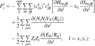 $$ F_i^l = - \mathop\sum\limits_{\rm{\lambda }}^{{\rm{ooc}}} {\mathop\sum\limits_{i{\rm{\alpha }}} {\mathop\sum\limits_{j{\rm{\beta }}} { ( {c_{i{\rm{\alpha }}}^{\rm{\lambda }} } )^* c_{j{\rm{\beta }}}^{\rm{\lambda }} } } } [ {{{\partial H_{i{\rm{\alpha }},j{\rm{\beta }}} } \over {\partial x^l }} - {\rm{\varepsilon }}_{\rm{\lambda }} {{\partial S_{i{\rm{\alpha }},j{\rm{\beta }}} } \over {\partial x^l }}} ] + {1 \over 2}\mathop\sum\limits_i {\mathop\sum\limits_{j \ne i} {{{\partial (N_i N_j V_N (R_{ij} ))} \over {\partial x^l }}} } \cr - {1 \over 2}\mathop\sum\limits_i {\mathop\sum\limits_{j \ne i} {Z_i Z_j {{\partial (E_0 /R_{ij} )} \over {\partial x^l }}} } ,\quad l = x,y,z\quad. \cr} $$
The computational efficiency and reliability of molecular dynamic scheme based on the SCED-LCAO Hamiltonian have been extensively tested for a variety of materials and validated against DFT calculations.Reference Leahy, Yu, Jayanthi and Wu29, Reference Yu, Wu and Jayanthi31, Reference Yu, Jayanthi and Wu41–Reference Tian, Yu, Leahy, Jayanthi and Wu43 Using the O(N)/SCED-LCAO, large-scale simulations containing 20,000 atoms of Si NWs have also been studied previously.Reference Yu, Wu and Jayanthi31 These methods are used in the present work for studying large diameter SiC NWs.