I. INTRODUCTION
Nanocrystalline diamond (NCD) films have many attractive properties, drawn from those of diamond whose exceptional properties are unsurpassed, suggesting many opportunities for application in a broad range of areas, such as optics, tribology, biomedicine, conformal coatings, and catalysis.Reference Gruen1–Reference Zhang, Su, Blume, Schlögl, Wang, Yang and Gajovic3 NCD is a nanocomposite material consisting of nanometer-sized diamond grains (or crystallites), which are surrounded by an amorphous carbon matrix.Reference Michaelson, Ternyak, Akhvlediani, Hoffman, Lafosse, Azria, Williams and Gruen4,Reference Mortet, Zhang, Eckert, D’Haen, Soltani, Moreau, Troadec, Neyts, De Jaeger, Verbeeck, Bogaerts, Van Tendeloo, Haenen and Wagner5 The diamond grains contain sp 3 hybridized carbon–carbon bonded atoms only, while the amorphous carbon phase consists of both sp 3 (diamond-like) and sp 2 (graphitic) hybridized carbon–carbon bonded atoms (and possibly hydrogen, in case of deposition in a hydrogen-rich atmosphere). Depending on the preparation method and conditions (especially in the presence of hydrogen), the amorphous carbon matrix fraction can be as high as 10% of NCD film volume or lower than 5%, resulting in almost pure NCD films.Reference Gruen1,Reference Klauser, Steinmuller-Nethl, Kaindl, Bertel and Memmel6,Reference Gruen7 The fraction of carbon atoms within the grain boundaries is inversely proportional to the radius of the diamond grain, assuming spherical grains.Reference Gruen7 For instance, a fraction of 10% of nondiamond carbon associated with an average crystallite size of 5 nm is reduced by tenfold, i.e., 1%, for a grain size of 50 nm.
NCD thin films have been prepared mostly using the chemical vapor deposition (CVD) method and variations thereof.Reference Davies8,Reference Spear and Dismukes9 More recent works using CVD include Refs. Reference Klauser, Steinmuller-Nethl, Kaindl, Bertel and Memmel6, Reference Gruen7, and Reference Donato, Faggio, Messina, Santangelo, Marinelli, Milani, Pucella and Verona-Rinati10–Reference Ballutaud, Jomard, Theys, Kociniewski, Rzepka, Girard and Saada14. Other deposition methods have been reported as well, such as pulsed laser deposition,Reference Hongyan, Jiajing and Guilong15,Reference Ou, Guo and Yan16 ion beam evaporation,Reference Pukha, Stetsenko, Dub and Lee17 sputtering,Reference Mounier, Bertin, Adamik, Pauleau and Barna18 and, very recently through our own efforts, the relatively novel pulsed electron beam ablation (PEBA).Reference Henda and Alshekhli19,Reference Alshekhli and Henda20 Most of the works have reported on NCD grown on silicon substrates with very few exceptions on other substrate systems, such as silicon oxide, silicon nitride, quartz, titanium nitride, molybdenum, and cemented carbide.Reference Popov, Bliznakov and Kulisch13 To our knowledge, no work has been reported on the potential effect of substrate on NCD films deposited by PEBA.
In view of the potential applications of NCD films, it is important to assess the influence of the type of substrate on the quality of films deposited by PEBA under the same process conditions. This study is a continuation of our previous efforts.Reference Henda and Alshekhli19,Reference Alshekhli and Henda20 Recently, the effects of electron beam accelerating voltage and beam pulse repetition rate on film properties have been elucidated.Reference Alshekhli and Henda20 In the present work, the substrate systems of interest include silicon, stainless steel, sapphire, and cubic boron nitride. These substrates are commonly used in a wide range of applications, such as microelectronics, optoelectronics, biomedical implants, tribology, and high-temperature environments. PEBA has proven to be a very attractive thin film preparation method as it has allowed the preparation of NCD films at room temperature and with very high content in sp 3 bonded carbon–carbon atoms (>96%).Reference Alshekhli and Henda20 PEBA is also readily scalable for potential commercial applications in addition to other advantages over existing physical vapor deposition (PVD)-based methods.Reference Harshavardhan, Strikovski and Goyal21,Reference Strikovski and Harshavardhan22 The deposited films have been analyzed using complementary analytical techniques, including visible-reflectance and visible-Raman spectroscopies, nanoindentation, atomic force microscopy (AFM), and scanning electron microscopy (SEM). The results from the different measurements are examined and discussed in terms of film properties, such as sp 3 content, hardness, thickness, morphology, grain size, and degree of crystallinity.
II. EXPERIMENTAL DETAILS
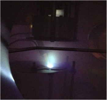
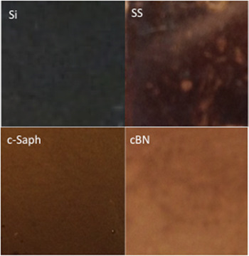
The deposition of thin films has been carried out in a channel-spark pulsed electron beam ablation system (PEBS-20, Neocera, Inc., Beltsville, MD). The pulsed electron beam source consists of a trigger, a hollow cathode, and a dielectric capillary tube, which is positioned at a 45° angle relatively to the target as shown in Fig. 1. The latter depicts the plume (greenish color) expanding vertically between the target (bottom) and substrate, over the duration of a single electron beam pulse. The source generates the pulses of electrons with the following features: ∼100 ns in pulse width, beam current ∼1 kA, and energy ∼15 keV. The ablated target is a 1-inch diameter highly ordered pyrolytic graphite (HOPG ZYB, Optigraph GmbH, Germany) disc. Silicon (100) (Si; Vin Karola), stainless steel 304 (SS; Valley Design), c-sapphire (c-Saph; Vin Karola), and cubic boron nitride (cBN; Henan Chinatex, China) of 1 cm2 × 1 mm or 1.5 cm2 × ½ mm in size have been used as substrates. All substrates have been sonically cleaned at 50 °C, then rinsed in acetone and followed with methanol and deionized water, just before they were transferred to the deposition chamber. Prior to deposition, the chamber was evacuated to a residual pressure of less than 1.33 × 10⁻³ Pa before backfilling with argon at a constant pressure of ∼0.5 Pa. All films have been deposited at room temperature, at a pulse frequency of 5 Hz and beam accelerating voltage of 14 kV. Before each deposition run, the target was preablated by 3000 electron beam pulses. The deposition time was set to ∼800 s, and the substrates have been loaded into the chamber at once. Figure 2 shows snapshots of films grown on the various substrates. The set of process conditions has been judiciously chosen, namely, so as to impart high pressure and high temperature to the ablated plasma particles upon impact on the substrate.Reference Alshekhli23 Model and calculation details will be elaborated upon in a separate study.
Snapshot of the inside of the chamber during a typical deposition run.

Snapshots of films deposited on various substrates. The four substrates are identified in the inset.

The morphology of the deposited films has been assessed using AFM (Bruker Multimode) and SEM (Model Quanta 250FEG, Hillsboro, OR, 10 kV). AFM images have been taken in contact mode using tapping mode etched silicon probe aluminum coating (TESPA) (doped Si, 333–382 kHz, 25 N/m) probe, at a scan rate of 0.5 Hz. The thickness of the films has been characterized via visible-reflectance spectroscopy, and obtained by fitting the generated experimental spectra (M-Probe Series, Semiconsoft) to calculated ones by means of a modified Marquardt–Levenberg minimization scheme using the built-in software (TFCompanion, Semiconsoft). Raman data have been collected in backscattered mode with a spectrometer (Horiba Jobin Yvon/XploRA) interfaced with an Olympus BX41 microscope (100x magnification, spot size ∼ 2 μm), at a grating of 1200, and an incident laser radiation wave length of 532 nm. Raman spectra (average of 10, 10 s spectra) have been generated within the range 50–1100 cm−1. Calibration has been carried out using the 521 cm−1 line of a silicon wafer. Hardness (HMT115) of the films (deposited on silicon, stainless steel, and sapphire) has been measured using a Shimadzu Ultra Micro Hardness Tester DUH-211S (Columbia, MD; Vickers tip, tip radius: 100 nm max). The experiments have been carried out using depth setting load–unload test.
III. RESULTS AND DISCUSSION
A. Visible-reflectance spectroscopy
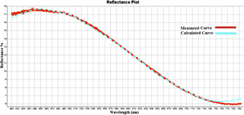
The thickness of the films, based on reflectance measurements, is listed in Table I. The thickness lies within the range of 72–89 nm with no clear trend differentiating the substrates. The reflectance of the films varies between about 3.5 and 8.5%, 17 and 8%, 0.5 and 4%, and 1 and 4.5% along the visible-light spectrum for silicon, stainless steel, sapphire, and cubic boron nitride, respectively, with higher reflectance from opaque substrates (Si, SS) relatively to the translucent ones (c-Saph, cBN). A typical reflectance spectrum record for the films on stainless steel is shown in Fig. 3. As can be seen, the agreement between measured and calculated reflectance responses is very good. All films are highly translucent as can be seen from Fig. 2. The brownish spots in the background of the snapshot of the film on cBN are due to silver paint used to glue the substrates onto the substrate holder, and, in the case of stainless steel, the whitish stains are the result of the substrate sonic cleaning process.
Results of Raman spectra deconvolution and film properties on various substrates. Si: Silicon (100), SS: stainless steel, c-Saph: c-Sapphire, cBN: Cubic boron nitride, I: peak intensity. Bare substrate roughness: Si: Ra ≅ 1 nm, SS: Ra ≅ 2 nm, c-Saph: Ra ≅ 1 nm, cBN: Ra ≅ 80 nm.

Visible-reflectance spectrum of NCD film on stainless steel substrate. Measured and calculated curves are shown.

B. Visible-Raman spectroscopy
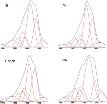
Chemical identification of the deposited films (mainly on silicon) using visible-Raman spectroscopy has been discussed at length in recent work, where more ample details can be found.Reference Alshekhli and Henda20 In the present work, the Raman spectra, shown in Fig. 4, obtained from the deposited films on the various substrates at a wave length of 532 nm, are composed of the typical features of NCD, which can be clearly distinguished after deconvolution of the entire band (using a mixed Gaussian–Lorentzian fit). The results of the deconvolutions of the spectra are summarized in Table I. The deconvoluted signals include the diamond peak at 1332 cm−1, the peak at 1150 cm−1 attributed to diamond nanocrystallites, the so-called G band (1536–1565 cm−1) and D band (1343–1378 cm−1) arising from disordered and/or amorphous carbon, and the band (1450–1463 cm−1) and peak at 1250 cm−1 attributed to t-PA (trans-polyacetylene).Reference Gruen7,Reference Ferrari and Robertson24–Reference Filik, Harvey, Allan and May27 The fraction of sp 3 carbon bonded atoms in the nanocomposite is a function of the G band, the diamond peak, and the NCD peak intensities, and has been estimated using the formula given by Ballutaud et al.Reference Ballutaud, Jomard, Theys, Kociniewski, Rzepka, Girard and Saada14 It is to be mentioned that Raman is a weak scatterer of sp 3 bonded carbon relatively to sp 2-bonded carbon, with a factor within the range of 50–230. In our calculations, we have used a conservative value of 75. The calculated values of the sp 3/(sp 2 + sp 3) ratio (i.e., sp 3 percentage) are listed in Table I. As can be observed, the type of bonding in the films is not influenced by the type of substrate since sp 3 percentage is practically the same (∼97–98%) irrespective of the substrate.
Deconvoluted Raman spectra of NCD film on various substrates (indicated in the inset). The horizontal axis is the wave length number in cm−1.

C. AFM and SEM
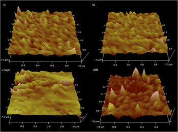
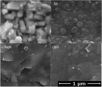
The morphologies of the films are depicted through their AFM topography in Fig. 5. For all substrates, the films consist of crystallites ranging in size between about 50 and 100 nm. The grain size features, as conventionally inferred from the Raman intensity ratio of diamond peak to diamond nanocrystallites peak, viz., I 1332/I 1150,Reference Klauser, Steinmuller-Nethl, Kaindl, Bertel and Memmel6 where I 1332 is the intensity of the diamond peak and I 1150 is the intensity of the diamond nanocrystallites peak, are listed in Table I. The nanocrystalline fraction has been inferred by calculating the ratio (I 1332 + I 1150)/Σ(I),Reference Popov, Bliznakov and Kulisch13 where the sum is over the intensities of all peaks of the entire spectrum. There are slight differences in grain size and crystallinity between the different substrates. The maximum difference is about 15% [i.e., (2.0–1.7)/2.0] in average grain size, and less than 3% (in absolute value, i.e., 93.5–90.8%) in nanocrystalline fraction, as per the respective data in Table I. In terms of film roughness, Ra (arithmetic mean roughness), no major differences exist between Si, SS, and c-Saph, see Fig. 5 and Table I. The rougher films on cBN are an artifact and commensurate with the high roughness of the bare substrate. SEM images of the films on the different substrates are shown in Fig. 6. For all substrates, the films consist of crystallites with an average size that is around or less than 100 nm. This finding is in good agreement with AFM results (Fig. 5) and Raman data, as reported in Table I. It is worth noticing that the crystallites seem to start as small nodules that coalesce to form larger clusters.
3D AFM topology of the films. The four substrates are identified in the inset.

SEM images of films on the different substrates as indicated in the inset.

D. Nanoindentation
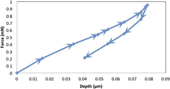
Nanoindentation is a common method used to measure the nanomechanical properties of thin films on substrates such hardness. A typical indentation load–displacement curve is shown in Fig. 7 and corresponds to films on stainless steel substrate. The maximum load is ∼1 mN during the indentation test. Hardness results of the nanoindented samples on silicon, stainless steel, and sapphire have been calculated for penetration depths slightly larger than their film thickness. The results of film hardness on various substrates are summarized in Table I. These results have been derived from the combined hardness of the whole assembly, i.e., NCD film on substrate. The hardness of the film has been estimated from a nondimensional relationship developed by Bhattacharya and Nix.Reference Bhattacharya and Nix28 Since the elastic modulus and yield stress of the film are not known beforehand, we have used the values of the ratio of the yield stress of substrate to that of the film and the ratio of the elastic modulus of the substrate to that of the film for bulk diamond. Substrate hardness data have also been obtained from the literature. The hardness of the films is within the range of 18.5–19.5 GPa, as listed in Table I, which is consistent with the hardness data of NCD films reported in the literature.Reference Yang, Lu and Cao29–Reference Wiora, Sadrifar, Brühne, Gluche, Fecht and Franek31 According to the data reported in Table I, film hardness seems to be relatively the same irrespective of the type of substrate used.
Loading–unloading versus penetration depth curve obtained from the indentation of NCD film on stainless steel. The arrows indicate the direction of the load–unload cycle.

The properties of films prepared by PEBA generally depend on many factors including ablated particle kinetic energy and density upon reaching the substrate (unchanged in this study as per constant electron beam energy density, target–substrate distance, and gas pressure), and deposition temperature (kept constant at room temperature). While different substrates have been used in the present work, it is worth noting that out of the four substrates (except sapphire) three crystallize in a cubic structure similar to diamond structure. Film roughness has been explained in terms of underlying substrate surface finish. It seems that, under the prevailing process conditions of the present study, the energy and density of particles impinging on a substrate are likely the controlling parameters in terms of the investigated film properties. This conclusion is at least in accordance with some recent calculations, based on plasma dynamics models and aided with the phase diagram of carbon, whereby we have estimated process conditions that are likely to result in diamond formation on substrates.Reference Henda and Alshekhli32 The fundamental idea is based on imparting the highest energy per carbon particle as the latter impinges on the substrate, in order for the ejected carbon particles to crystallize in the diamond structure. Our model calculations have shown that under judiciously selected process conditions (similar to ones used in the present work), the temperature (T) and pressure (P) of ejected plasma nanoparticles upon impact with the substrate lead to the formation of diamond as per the phase diagram of carbon (T, P).
IV. CONCLUSIONS
Thin films (∼70–90 nm) of NCD have been deposited on various substrates by PEBA, and characterized by visible-reflectance spectroscopy, visible-Raman spectroscopy, AFM, and SEM. Based on measurement data, film properties such as thickness, hardness, morphology, grain size, sp 3 content, and degree of crystallinity have been estimated. Irrespective of the substrate, the films consist of diamond nanocrystallites with sp 3 content of ∼97–98% and average particle size ranging within the nanoscale (<100 nm) and exhibit hardness within the range of 18.5–19.5 GPa. The bonding type in the films, grain size, and degree of crystallinity are not appreciably influenced by the substrate as shown from Raman spectroscopy data. On the basis of the presented data and from the comparison of the different properties with respect to the type of substrate used, it can be concluded that the substrate material does not appear to appreciably affect overall film quality.
ACKNOWLEDGMENTS
This research has been supported by the Canada Foundation for Innovation (CFI) and the Natural Sciences and Engineering Research Council of Canada (NSERC).