
Introduction
Since two-thirds of chemical energy from fossil fuels have been exhausted as heat energy without use, much attention has been paid to thermoelectric technology which can convert heat energy into electric energy and vice versa.[Reference Toshima, Imai and Ichikawa1, Reference Toshima, Oshima, Anno, Nishinaka, Ichikawa, Iwata and Shiraishi2] The performance of thermoelectric materials is determined by a dimensionless figure of merit, ZT, which is defined as σS 2 T/κ, where σ is the electrical conductivity, S is the Seebeck coefficient, T is the absolute temperature, κ is the thermal conductivity, and σS 2 represents the power factor. Materials are required to have a higher power factor and lower thermal conductivity to gain a higher ZT value.[Reference Li, Liu, Zhao and Zhou3, Reference Luo, Billep, Waechtler, Otto, Toader, Gordan, Sheremet, Martin, Hietschold, Zahn and Gessner4]
Inorganic thermoelectric materials such as bismuth telluride (Bi2Te3) and bismuth selenide (Bi2Se3) have been investigated intensively and developed for commercial applications at room temperature.[Reference Satterthwaite and Ure5–Reference Ohnuma and Iwasaki8] Despite the high-power factor and figure of merit, inorganic materials have several disadvantages such as difficulty in the mass production of devices due to their poor formability.
Increasing attention has been paid to organic thermoelectric materials because of their various advantages over inorganic thermoelectric materials. Especially, their flexibility enables us to set thermoelectric materials easily on any surface with shapes of variety, and also their low thermal conductivity is attractive to achieve a better thermoelectric property. Although conductive polymers like poly(3,4-ethylenedioxythiophene)-poly(styrenesulfonate) (PEDOT-PSS) are promising p-type flexible thermoelectric materials,[Reference Luo, Billep, Waechtler, Otto, Toader, Gordan, Sheremet, Martin, Hietschold, Zahn and Gessner4, Reference Bubnova, Khan, Malti, Braun, Fahlman, Berggren and Crispin9, Reference Kim, Shao, Zhang and Pipe10] it is still not easy to use them for mass production due to the higher prices compared with ordinary polymers (i.e., insulating polymers). Furthermore, the development of n-type flexible materials is desirable for the design of π-shaped thermoelectric modules in which thermoelectric couples that consist of n-type (containing free electrons) and p-type (containing free holes) thermoelectric elements are connected electrically in series and thermally in parallel,[Reference Snyder and Toberer6, Reference Kim, Kikuchi, Itoh, Iida and Taya11, Reference Nonoguchi, Ohashi, Kanazawa, Ashiba, Hata, Nakagawa, Adachi, Tanase and Kawai12] but there has been essentially no report on the synthesis of such n-type materials from ordinary polymers in spite of successes of several earlier studies on the development of n-type organic thermoelectric materials.[Reference Nonoguchi, Ohashi, Kanazawa, Ashiba, Hata, Nakagawa, Adachi, Tanase and Kawai12–Reference Ohnuma and Iwasaki16]
Compared with other nanostructures, metal nanoparticles [such as gold (Au), silver (Ag), and copper (Cu)] have proven to be the flexile nanostructures owing to the synthetic control of their size, shape, assembly, and encapsulation.[Reference Huang, Jain, El-Sayed and El-Sayed17–Reference Ohnuma, Yamamoto, Kozawa and Ohtani22] Au nanoparticles are especially promising because of their inertness, non-toxicity, and simple and fast preparation.[Reference Huang, Jain, El-Sayed and El-Sayed17, Reference Ghosh, Han, De, Kim and Rotello23]
In the present study, therefore, we tried to fabricate a new type of n-type flexible film with a double-layer structure by hybridizing an n-type inorganic thermoelectric material, Bi2Se3, and an ordinary insulating polymer, poly(vinyl alcohol) (PVA), and examined the thermoelectric properties. The particular arrangement of Bi2Se3 nanoflakes with/without Au-nanoparticles modification in the hybrid film and the dependence of the thickness of layer structures on the preparation conditions were also investigated.
Experimental
Chemical and materials
All chemicals were of reagent-grade and were used without further purification. Sodium selenite (Na2SeO3, ≥97.0%) was purchased from Sigma-Aldrich, St. Louis, USA. Bismuth nitrate pentahydrate (Bi(NO3)3·5H2O, ≥99.5%), hydroxylamine (NH2OH, 50 wt.% in H2O), PVA (completely hydrolyzed, average polymerization degree ~400–600, saponification degree ≥96.0 mol.%), trisodium citrate anhydrous (Na-CA, ≥99.0%), tetrachloroauric acid tetrahydrate (≥99.9%), ethylene glycol (EG, ≥99.5%), and acetone (≥99.0%) were purchased from Wako Pure Chemical Industries, Osaka, Japan. Deionized water was obtained by a water purifier (RFP343RB, Advantec, Tokyo, Japan) and is referred to as water throughout the manuscript.
Synthesis of Bi2Se3 nanoflakes
Bi2Se3 nanoflakes were prepared using the method reported by Min.[Reference Min, Roh, Yang, Park, Kim, Hwang, Lee, Lee and Jeong7] In a typical synthesis, a solution of Na2SeO3 (0.49 g in 60 mL of EG) was poured in 200 mL round-bottom flask, followed by the addition of a solution of Bi(NO3)3·5H2O (0.91 g (1.9 mmol) in 15 mL of EG) under magnetic stirring at room temperature. The flask was heated to the 180 °C under nitrogen environment and then, NH2OH solution (1.9 mL in 8.1 mL of EG) was injected to the mixture. The reaction was allowed to proceed for 30 min and cooled down to room temperature. The product was washed by dispersion–centrifugation process in a mixture of acetone and water (60:40 v/v), and it was then dried under vacuum overnight at room temperature.
Modification of Bi2Se3 nanoflakes with Au nanoparticles
Bi2Se3 nanoflakes were modified with Au nanoparticles according to a previously described procedure.[Reference Ohnuma and Iwasaki8] To an aqueous Au precursor solution (0.08 mM, 19 mL) heated to boiling was added 2.3 mL of aqueous solution containing both Na-CA (38.8 mM) and Bi2Se3 nanoflakes (100 mg), and the solution was then boiled for further 30 min. After cooling, the product was washed with water, and it was then dried under vacuum at room temperature.
Fabrication of hybrid films from Bi2Se3 nanoflakes/Au-modified Bi2Se3 nanoflakes and PVA
The hybrid films were typically prepared by drop-casting the mixed dispersion of Bi2Se3 nanoflakes/Au-modified Bi2Se3 nanoflakes (17 mg) and PVA (15 mg) in water (0.7 mL) on a stainless substrate overnight at 50 °C.
Thermoelectric properties measurements
The thermoelectric properties involving electrical conductivity and Seebeck coefficient of the hybrid films were measured at room temperature using a Hall coefficient measurement system (ResiTest8340, Toyo) and a thermoelectric measurement system (ZEM-3, ULVAC), respectively, in the ambient atmosphere.
Characterizations
Scanning electron microscopy (SEM) and energy-dispersive spectrometry (EDS) analyses were performed using a JEOL JSM-7500F equipped with JEOL JED-2300. The acceleration voltage was 15 kV. The film samples were coated with thin layers of osmium (5, 8 nm in thickness for the bottom side, cross-section, respectively) before imaging. The hydrodynamic diameters and zeta potential of the nanoparticles were measured by dynamic light scattering using a Malvern Zetasizer Nano ZS at 25 °C.
Results and discussion
Fabrication of the hybrid film from Bi2Se3 nanoflakes and PVA
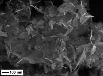
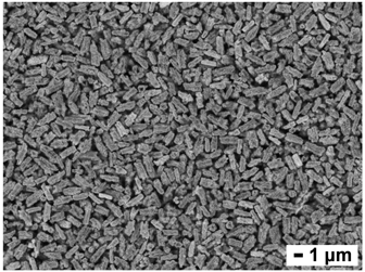
Figure 1 shows the SEM image of Bi2Se3 nanoflakes that were used for the fabrication of the hybrid film. The nanoflakes had a flat shape (thickness: ~10 nm) with an average hydrodynamic diameter of 270 nm in EG (see Fig. S1). When we dispersed the Bi2Se3 nanoflakes in water, the nanoflakes tended to reduce the surface area due to interfacial tension between water and the surface of the particles, and the size distribution was thus drastically changed as a result of the formation of pillar-shaped assemblies (length: ~2 µm, width: ~1 µm) and the aggregation of those with unassembled Bi2Se3 nanoflakes (see Fig. S2).
SEM image of flake-shaped Bi2Se3 nanoparticles (Bi2Se3 nanoflakes). The average hydrodynamic diameter of Bi2Se3 nanoflakes was 270 nm.

Because such a large particle assembly could preferentially sediment during the drying process of an aqueous dispersion,[Reference Cardinal, Jung, Ahn and Francis24] we tried to utilize this phenomenon for the preparation of a hybrid film with a double-layer structure in which Bi2Se3 nanoflakes are located in the lower part of PVA matrix. In the hybrid film, the electrical connection between Bi2Se3 nanoflakes might be existed, and it was expected that the thermoelectric properties derived from the pillar-shaped assemblies, which might have unique characteristics as a hierarchical structure from nanomaterials,[Reference Amano, Nogami, Abe and Ohtani25, Reference Hu, Zhong, Zheng, Huang, Zhang and Chen26] would be measured from the bottom side of the hybrid film.
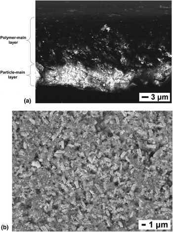
Figure 2(a) shows a back-scattering SEM image of the cross-section of the hybrid film from Bi2Se3 nanoflakes and PVA (Bi2Se3/PVA hybrid film, the bright (white) regions correspond to Bi2Se3). The internal structure of the hybrid film can be classified into two layers as we expected. One is the polymer-main layer (upper layer) in which PVA is the main component besides the existence of a small amount of Bi2Se3 nanoflakes, and the other is the particle-main layer (lower layer) in which Bi2Se3 nanoflakes were preferentially distributed in the PVA matrix. The thickness of the particle-main layer was ~10 µm. Although the volume fraction of Bi2Se3 nanoflakes in the hybrid film was as high as 17%, it was a self-standing flexible film without any visible cracks. It seems to be that the mechanical strength of PVA works as a support of the hybrid structure. Figure 2(b) shows a back-scattering SEM image of the bottom side of Bi2Se3/PVA hybrid film. The pillar-shaped assemblies of Bi2Se3 nanoflakes and unassembled Bi2Se3 nanoflakes were observed, and the two-dimensional packing fraction of such particles was 71% (analyzed using a software (Asahi Kasei Engineering A-Zou Kun)). As shown in Table I entry 1, the bottom side of the hybrid film exhibited a relatively high Seebeck coefficient (S = –73 µV/K) as an n-type film, and the value is even higher than that of polycrystalline Bi2Se3 (i.e., sintered Bi2Se3, S = ~–60 µV/K) in Ref. Reference Min, Roh, Yang, Park, Kim, Hwang, Lee, Lee and Jeong7. On the other hand, the electrical conductivity (evaluated on the assumption that the thickness of the electrically conductive part was 10 µm) was low (σ = 3.04 × 10⁻² S/cm) perhaps due to a poor electrical contact by the existence of the irregular-shaped aggregation with unassembled Bi2Se3 nanoflakes, and it was calculated that the power factor was 1.6 × 10⁻⁸ W/m/K2. Besides that, the top side of the hybrid film was electrically inactive.
Back-scattering SEM images of the hybrid film from Bi2Se3 nanoflakes and PVA (Bi2Se3/PVA hybrid film, (a) cross-section and (b) bottom side of the hybrid film, respectively). The bright (white) regions correspond to Bi2Se3.

Electrical properties of hybrid films at room temperature (Bi2Se3 nanoflakes with the average hydrodynamic diameter of 270 nm were used for both samples).

Fabrication of the hybrid film from Au-modified Bi2Se3 nanoflakes and PVA
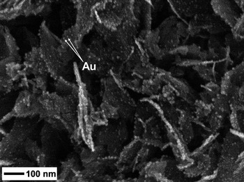
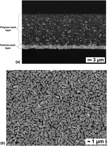
We next tried to modify the Bi2Se3 nanoflakes dispersed in water with Au nanoparticles via liquid-phase reductive deposition to prevent the aggregation of the pillar-shaped assemblies with unassembled Bi2Se3 nanoflakes by using the relatively high zeta potential derived from Au nanoparticles (>~40 mV).[Reference Park and Hamad-Schifferli27, Reference Doane, Chuang, Hill and Burda28] Figure 3 shows an SEM image of Au-modified Bi2Se3 nanoflakes. Interestingly, different from our results with Bi2Te3 nanoflakes,[Reference Ohnuma and Iwasaki8] Au nanoparticles, confirmed by EDS analysis (see Fig. S3), were evenly distributed on the surface of Bi2Se3 nanoflakes and the diameters were ~3–20 nm. The zeta potential of the aqueous dispersion of Au-modified Bi2Se3 nanoflakes was −43.5 mV. Figure 4(a) shows a back-scattering SEM image of the cross-section of the hybrid film from Au-modified Bi2Se3 nanoflakes and PVA (Au-modified Bi2Se3/PVA hybrid film, the bright (white) regions correspond to Au-modified Bi2Se3). The hybrid film also had a double-layer structure consisting of a polymer-main layer and a particle-main layer; on the other hand, the thickness of the particle-main layer became thinner (thickness: ~3 µm) compared with the case of Bi2Se3/PVA hybrid film. It was also a self-standing flexible film (see Fig. S4) without any visible cracks in spite of the high-volume fraction of Bi2Se3 nanoflakes (17%). Figure 4(b) shows a back-scattering SEM image of the bottom side of Au-modified Bi2Se3/PVA hybrid film (see Fig. S5 for more images). The pillar-shaped assemblies were dominant at the bottom side of the hybrid film as a result of selective sedimentation of the pillar-shaped assemblies derived from the successful separation of unassembled nanoflakes from the assemblies. The two-dimensional packing fraction of particles was improved to 88% (analyzed using A-Zou Kun). As shown in Table I entry 2, the bottom side of the hybrid film exhibited a higher Seebeck coefficient (S = –91 µV/K) than that of the film without Au nanoparticles, and it is one of the highest values as a self-standing n-type flexible film to our knowledge. The electrical conductivity (evaluated on the assumption that the thickness of the electrically conductive part was 3 µm) was also improved to 2.25 S/cm due to a better electrical contact between the pillar-shaped assemblies, and it was calculated that the power factor was 1.9 × 10⁻⁶ W/m/K2. It should be mentioned that both the electrical conductivity and power factor of the hybrid film are still worse than those of polycrystalline Bi2Se3 (σ = ~240 S/cm, σS 2 = ~1.0 × 10⁻⁴ W/m/K2) in Ref. Reference Min, Roh, Yang, Park, Kim, Hwang, Lee, Lee and Jeong7. In addition, the top side of the hybrid film was also electrically inactive in the same way as the film without Au nanoparticles.
SEM image of Bi2Se3 nanoflakes modified with Au nanoparticles (Au-modified Bi2Se3 nanoflakes). The Au nanoparticles were ~3–20 nm in diameter.

Back-scattering SEM images of the hybrid film from Au-modified Bi2Se3 nanoflakes and PVA (Au-modified Bi2Se3/PVA hybrid film, (a) cross-section and (b) bottom side of the hybrid film, respectively). The bright (white) regions correspond to Au-modified Bi2Se3.

Dependence of the thickness of layer structures in Au-modified Bi2Se3/PVA hybrid film on the preparation conditions
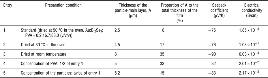
Since the thickness of the particle-main layer in the Au-modified Bi2Se3/PVA hybrid film should be bigger for the design of the smaller thermoelectric devices, we next examined the dependence of the thickness of layer structures in Au-modified Bi2Se3/PVA hybrid film on the preparation conditions (such as drying temperature, concentration of PVA, and concentration of particles). We used Bi2Se3 nanoflakes with an average hydrodynamic diameter of 250 nm for this comparative experiment. Table II shows the results including the electrical properties at room temperature. We found that the thickness of layer structures could be tailored by setting the drying temperature lower, decreasing the concentration of PVA, or increasing the concentration of the particles. The thickest particle-main layer (thickness: ~8 µm) was observed when the drying temperature was room temperature (entry 3). A systematic study is under way to achieve a complete understanding of the correlation between the thickness of the particle-main layer and the electrical properties.
Thickness of the particle-main layer and electrical properties (at room temperature) of Au-modified Bi2Se3/PVA hybrid films prepared with different conditions (Bi2Se3 nanoflakes with the average hydrodynamic diameter of 250 nm were used for this comparative experiment).

Conclusions
We have fabricated a new type of n-type flexible film with a double-layer structure consisting of a polymer-main layer and a particle-main layer by hybridizing an n-type inorganic thermoelectric material, Bi2Se3, and an ordinary insulating polymer, PVA. To utilize the mechanical property of PVA for the flexibility of the hybrid film, Bi2Se3 nanoflakes were distributed in the one side of PVA film. We have also found that the arrangement of Bi2Se3 nanoflakes in the hybrid film could be tailored by the modification with Au nanoparticles, and Au-modified Bi2Se3/PVA hybrid film showed a high Seebeck coefficient (S = −91 µV/K at room temperature) as a self-standing n-type flexible film. Furthermore, lower drying temperature, smaller concentration of PVA, and bigger concentration of the particles in the preparation condition of Au-modified Bi2Se3/PVA hybrid film were favorable for the formation of a thicker particle-main layer. We believe that the approach described in this study could be extended to other kinds of hybrid films from a variety of inorganic and organic materials. Our method is expected to be used for the design of flexible functional devices such as π-shaped thermoelectric modules from p- and n-type flexible materials.
Supplementary material
The supplementary material for this article can be found at https://doi.org/10.1557/mrc.2018.128.
Acknowledgment
This work was partly supported by the Nanotechnology Platform Program (Molecule and Material Synthesis) of the Ministry of Education, Culture, Sports, Science and Technology (MEXT), Japan.