Motivation
Diamond possesses remarkable physical and chemical properties and in many ways is the ultimate engineering material, often termed “the engineer’s best friend.” It has high mechanical hardness (10,000 kg mm–2), high Young’s modulus (1050 GPa), high thermal conductivity (22 W cm–1 K–1), low thermal expansion coefficient, high breakdown field (>10 MV cm–1), and high carrier mobility (4500 cm2 V–1 for electrons and 3800 cm2 V–1 for holes).Reference Isberg, Hammersberg, Johansson, Wikström, Twitchen, Whitehead, Coe and Scarsbrook 1 It is biocompatible and chemically inert. Optically, diamond is transparent from the UV to IR, has a high refractive index (n = 2.4), large Raman gain (15–75 cm GW–1),Reference Feve, Shortoff, Bohn and Brasseur 2 large intensity-dependent refractive index (n 2 = 1.3 × 10⁻¹⁹ m2 W–1), and a wide variety of light-emitting defects.Reference Zaitsev 3 These properties make diamond a highly desirable material for many applications, including high-frequency micro- and nanoelectromechanical systems, nonlinear optics, magnetic and electric field sensing, and biomedicine (e.g., cell labeling/monitoring, biosensing, and drug delivery).
One particularly exciting application of diamond is in the field of quantum information science and technology (QIST), which promises realization of powerful quantum computers capable of tackling problems that cannot be solved using classical approaches, as well as realization of secure communication channels. At the heart of these applications is diamond’s luminescent crystalline defects—color centers—and the nitrogen-vacancy (NV) color center in particular. This atomic system in the solid-state possesses all the essential elements for QIST, including storage, logic, and communication of quantum information. Quantum information can be stored in the electron spin of the NV or the nuclear spin of nearby atoms, with very long lifetimes even at room temperature.Reference Maurer, Kucsko, Latta, Jiang, Yao, Bennett, Pastawski, Hunger, Chisholm, Markham, Twitchen, Cirac and Lukin 4 Quantum logic can be achieved via the application of microwave and RF fields to drive transitions between these electron and nuclear spin sublevels.Reference Dutt, Childress, Jiang, Togan, Maze, Jelezko, Zibrov, Hemmer and Lukin 5 – Reference van der Sar, Wang, Blok, Bernien, Taminiau, Toyli, Lidar, Awschalom, Hanson and Dobrovitski 7 Finally, spin quantum information can be communicated via spin-dependent fluorescence intensity, resulting in a source of spin-photon entangled pairs.Reference Togan, Chu, Trifonov, Jiang, Maze, Childress, Dutt, Sørensen, Hemmer, Zibrov and Lukin 8
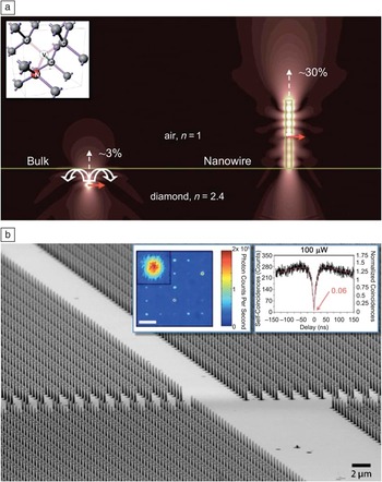
However, these and other applications depend crucially on the efficiency with which information can be exchanged between the NV center’s electron spin (a stationary qubit in the context of quantum computation) and a photon (a ‘‘flying’’ qubit). Therefore, the ability to efficiently excite the NV center and readout its spin state optically is of central importance. Unfortunately, in the case of NV centers in a bulk diamond substrate, this process is affected by the total-internal reflection at the diamond-air interface, due to the large refractive index of diamond (n = 2.4), resulting in a typical photon collection efficiency of ∼3% ( Figure 1 a). Moreover, the NV-photon interaction in a particular transition that is of interest for quantum information applications, the zero-phonon line (ZPL), is relatively weak compared to other photonic transitions. Therefore, there has been great interest in increasing the photon–NV center interaction using photonic engineering that enables the following important features:
-
1. Efficient interface between the macroscopic world (lenses, fibers, etc.) and the atomic scale of NV centers. This allows for efficient exchange of information between photons and NV spins by improving the efficiency with which information is stored (photon → NV spin) and read out (NV spin → photon).
Figure 1.Diamond nanowires. (a) Emission profiles of a nitrogen vacancy (NV) embedded in bulk diamond crystal (left) and a diamond nanowire (right), obtained using finite-difference time-domain modeling. Position and orientation of the NV dipole is indicated by the red arrows. Collection efficiency for photons emitted by an NV (inset) in a bulk diamond crystal is low (∼3%) due to the total internal reflection at the diamond-air interface. The collection efficiency can be increased 10 times (∼30%) using diamond nanowires. n, refractive index. (b) Scanning electron microscopy image of diamond nanowires, ∼2 μm tall and 200 nm in diameter, fabricated in single crystal diamond. Inset shows a confocal image of a 5 × 5 array of nanowires—each bright spot corresponds to a nanowire with a single NV center. Photon antibunching, indicative of single photon emission, is also shown for one of the nanowires (inset plot).

-
2. Engineering of the emission rate and spectrum of the NV and, in particular, enhancement of its ZPL emission via the Purcell effect.Reference Purcell 9
-
3. Scalable fabrication techniques that allow for realization of many devices in parallel.

A system with all of these features may ultimately enable important feats such as fast and efficient spin readout, scalable quantum-optical interconnects, high sensitivity field probes,Reference Balasubramanian, Chan, Kolesov, Al-Hmoud, Tisler and Shin 10 – Reference Bernien, Childress, Robledo, Markham, Twitchen and Hanson 13 and efficient entanglement generation.Reference Togan, Chu, Trifonov, Jiang, Maze, Childress, Dutt, Sørensen, Hemmer, Zibrov and Lukin 8 , Reference Neumann, Mizuochi, Rempp, Hemmer, Watanabe, Yamasaki, Jacques, Gaebel, Jelezko and Wrachtrup 14
Due to difficulties associated with the fabrication of nanoscale optical devices in diamond, however, early approaches to photonic engineering have mostly relied on hybrid platforms that combine diamond nanocrystals or bulk diamond substrates with external optical devices fabricated in non-diamond materials.Reference Park, Cook and Wang 15 – Reference Schietinger, Barth, Aichele and Benson 21 The former, however, suffer from inferior optical and spin properties of NV centers in nanocrystals, whereas the latter suffer from reduced overlap between the optical field and NV center. Therefore, an enticing approach is to fabricate optical devices directly in diamond and embed individual color centers inside them. In this article, we summarize recent efforts aimed at achieving these goals, and review recent developments in the emerging and exciting field of diamond quantum photonics.
Broadband approaches to large collection efficiency: Diamond nanowires
The simplest optical structure that can overcome the total-internal reflection limitations, and thus significantly increase the collection efficiency of photons emitted from a NV, is a diamond nanowire (Figure 1).Reference Hausmann, Khan, Zhang, Babinec, Martinick, McCutcheon, Hemmer and Loncar 22 , Reference Babinec, Hausmann, Khan, Zhang, Maze, Hemmer and Loncar 23 The nanowire, here a 2 μm tall and 200 nm diameter pillar etched into the surface of bulk single crystal diamond substrate, has two roles: (1) It acts as a waveguide that collects photons emitted from an embedded NV center, and (2) it acts as a dielectric antenna and channels photons emerging from the top of the nanowires facet into the collection optics with >90% efficiency. Using numerical modeling, we estimate that a total of ∼30% of all emitted photons can be collected (Figure 1a) by a microscope objective with a numerical aperture of 0.95, which is an order of magnitude improvement over the collection efficiency of NVs in bulk diamond. This prediction was confirmed experimentally,Reference Babinec, Hausmann, Khan, Zhang, Maze, Hemmer and Loncar 23 and we found that nanowire geometry allows us to register 200,000–300,000 photon counts per second (CPS), compared to ∼30,000 CPS in the case of bulk diamond. Important aspects of a diamond nanowire approach are the fabrication simplicity and scalability—millions of nanowires can be fabricated in parallel on the same chip using conventional top-down nanofabrication techniques based on electron beam lithography and reactive ion etching (Figure 1b). Diamond nanowires are ideally suited for applications where large numbers of indistinguishable photons are needed, including entanglement generation. Furthermore, the nanowire geometry is of great interest for applications such as magnetometry and near-field magnetic sensing.Reference Maletinsky, Hong, Grinolds, Hausmann, Lukin, Walsworth, Loncar and Yacoby 24 One potential drawback of the nanowire geometry for applications in QIST is the proximity of the diamond surface to the NV center. NVs close to the diamond surface can suffer from surface-charge fluctuations, which can result in blinking (jumps between the negatively charged (NV–) and neutral (NV0) states) and spectral diffusion (jumps in NV energy levels). These effects can be minimized by engineering diamond’s material properties via nitrogen doping, annealing at high temperatures, and appropriate surface terminations (see the article by Wrachtrup et al. for details). Alternatively, a solid immersion lens (SIL) geometry, a hemisphere etched into the diamond surface, can be used instead of the nanowire geometry.Reference Robledo, Childress, Bernien, Hensen, Alkemade and Hanson 12 , Reference Bernien, Childress, Robledo, Markham, Twitchen and Hanson 13 , Reference Siyushev, Kaiser, Jacques, Gerhardt, Bischof, Fedder, Dodson, Markham, Twitchen, Jelezko and Wrachtrup 25 , Reference Hadden, Harrison, Stanley-Clarke, Marseglia, Ho, Patton, O’Brien and Rarity 26 SILs allow collection efficiencies comparable to those of nanowires, but with NVs further away from diamond-air interfaces, thus minimizing the negative impact of surfaces on the stability of NVs. The drawback of SIL geometry is a more complicated fabrication approach, often based on focused ion beam milling.
Control of NV radiative rates using metallic nanocavities
While diamond nanowire geometry offers a large increase in photon collection efficiency of emitted photons, it does not provide much freedom for engineering of the radiative rate of the emission process. The latter, however, is important in order to increase the rate of specific optical transitions of the NV, and ZPL in particular, which can be achieved by coupling the NV center to a host cavity. The cavity can provide an increase in the photon emission rate by the Purcell factor (F P), which is proportional to the Q/V ratio, where Q is the quality factor, describing the lifetime of photons in the cavity, and V is the mode volume of the cavity.Reference Vahala 27 Therefore, a large F P can be obtained by realizing cavities with either tiny V or ultrahigh Q.
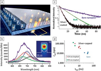
One promising and simple approach to achieve nanocavities with small V is to use metals as cladding material ( Figure 2 ).Reference Bulu, Babinec, Hausmann, Choy and Loncar 28 , Reference Choy, Hausmann, Babinec, Bulu, Khan, Maletinsky, Yacoby and Loncar 29 Recently, nanocavities consisting of ∼100 nm tall diamond nanoposts embedded within a thick (∼1 μm) silver layer were fabricated, which support resonance with a mode volume of 0.07 (λ/n)3 (n–refractive index of diamond), and a quality factor of ∼10. The cavity provides excellent spatial overlap between the highly localized optical field and the enclosed NV dipole. These effects combined resulted in enhancement of the spontaneous emission (SE) rate of the embedded NV center with an experimentally measured Purcell factor of F P ∼ 10 (theoretical F P∼ 30). However, this simple geometry suffers from a reduced photon extraction/collection efficiency because NV centers can also emit into surface plasmons at the diamond-silver interface, which in this case represents one of the loss mechanisms. To scatter these plasmons out and improve the collection efficiency to above 30%, concentric metallic gratings can be used.Reference Bulu, Babinec, Hausmann, Choy and Loncar 28
Diamond-silver nanocavities consist of (a) diamond nanoposts embedded in silver. (b) The emission spectrum of nitrogen vacancies (NVs) in bulk (purple line) and embedded in four different cavities with slightly different geometry (solid red, blue, green, and black lines). The cavities modify the emission spectrum as well as (c) radiative lifetimes of embedded NVs, which can be as short as 2.5 ns. Interestingly, bare diamond nanoposts (without silver) prolong the NV lifetime to ∼50 ns from its bulk value of ∼16 ns. (d) The number of collected photons I sat for several diamond-silver nanocavities with slightly different geometry (due to fabrication tolerances) and different implantation depth (indicated in the legend). As expected, I sat increases as the radiative time τNV of the NV is reduced.

Integrated diamond photonics
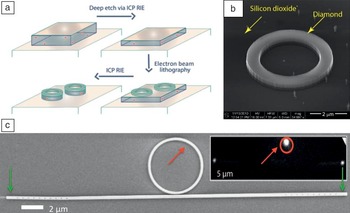
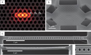
Both platforms discussed so far are tailored to applications requiring channeling photons to free space. In contrast, often it is of interest to keep the photons on-chip and take advantage of chip-scale integrated nanophotonics for information routing. All the current platforms for integrated photonics are based on the availability of the optical material in the form of a thin membrane. For example, in the case of silicon photonics, large-area submicron-thick membranes are realized by ion slicing followed by wafer bonding. In the case of III–V semiconductor photonics, the light-guiding layer can be epitaxially grown on top of a low-index or sacrificial substrate. Currently, monocrystalline diamond material is not readily available in the form of submicron-thick membranes, but many methods have been investigated for producing such membranes (see Reference 30 for an extensive review). An ion-slicing method, similar to that used to fabricate the silicon-on-insulator platform, has been applied to diamond,Reference Magyar, Lee, Limarga, Aharonovich, Rol, Clarke, Huang and Hu 31 , Reference Bayn, Meyler, Lahav, Salzman, Kalish, Fairchild, Prawer, Barth, Benson, Wolf, Siyushev, Jelezko and Wrachtrup 32 but so far the optical properties of the diamond membranes fabricated this way do not match those of single crystal diamond. Another promising approach for single crystal diamond membranes is based on epitaxial deposition on silicon via iridium/yttria-stabilized zirconia buffer layers.Reference Gsell, Bauer, Goldfuss, Shreck and Strizker 33 This approach has been used successfully to fabricate photonic crystal devices in single crystal diamond that showed resonances with quality factors of a few hundred ( Figure 4 c).Reference Riedrich-Möller, Kipfstuhl, Hepp, Neu, Pauly, Mücklich, Baur, Wandt, Wolff, Fischer, Gsell, Schreck and Becher 34 Focused ion beam milling has also been used to carve freestanding photonic crystal cavities out of bulk diamond substrates, though with limited success.Reference Babinec, Choy, Smith, Khan and Loncar 35 , Reference Bayn, Meyler, Salzman and Kalish 36 To date, the highest quality photonic devices have been fabricated from submicron-thick diamond membranes obtained by thinning diamond slabs using reactive ion etching. These diamond slabs, with an initial thickness of 5–20 microns, are available from commercial vendors such as Element Six. During fabrication, the diamond slab is mounted on a low index substrate (such as silicon dioxide). The diamond photonic devices are then fabricated using a variety of techniques based on electron beam lithography and dry reactive ion etching ( Figure 3 a).Reference Faraon, Barclay, Santori, Fu and Beausoleil 37 – Reference Hausmann, Shields, Quan, Maletinsky, McCutcheon, Choy, Babinec, Kubanek, Yacoby, Lukin and Loncar 39 This approach was used to realize diamond ring resonators (Figure 3b) with quality factors as high as 25,000 (at a 637 nm wavelength).Reference Faraon, Barclay, Santori, Fu and Beausoleil 37 By combining ring resonators with optical waveguides and grating couplers, an integrated on-chip optical network was realized and was used to demonstrate generation and routing of single-photon fields (Figure 3c).Reference Hausmann, Shields, Quan, Maletinsky, McCutcheon, Choy, Babinec, Kubanek, Yacoby, Lukin and Loncar 39 Finally, photonic crystal cavities (intentional defects in a two-dimensional periodic lattice of holes patterned in a diamond membrane) with quality factors Q ∼ 3,000 were realized using a similar approach ( Figure 4 a–b). Coupling between a NV center and the cavity mode was observed, resulting in the enhancement of the overall NV brightness and the ZPL emission in particular.Reference Faraon, Santori, Huang, Acosta and Beausoleil 38 The planar photonic crystal platform allows for straight-forward on-chip integration of photonic components (resonators, waveguides, modulators, add/drop filters, etc.) in an optical network and thus is likely going to play an important role in future QIST applications of diamond.
(a) Fabrication procedure used to realize photonic devices in thin single crystal diamond films using inductively coupled plasma reactive ion etching (ICP RIE) and electron beam lithography. (b) Diamond ring resonator located on top of a silicon dioxide layer. (c) Integrated on-chip diamond network composed of a diamond ring resonator coupled to a ridge waveguide with grating couplers at its ends. Inset: Single photons are generated by a nitrogen vacancy embedded inside the ring (red circle and red arrows), routed into the diamond waveguide, and finally scattered out using grating couplers (green arrows).

(a) Simulation showing the electric field density for the fundamental mode of a linear three hole defect photonic crystal cavity in diamond. (b) Photonic crystal cavity fabricated in a single crystal diamond membrane (thickness ≈200 nm) obtained using the approach described in Figure 3a. The photonic crystal cavity parameters are: periodicity ≈218 nm and hole radius ≈63 nm. (c) One-dimensional photonic crystal cavity fabricated in single crystal diamond using focused ion beam milling. Reprinted with permission from Reference Reference Riedrich-Möller, Kipfstuhl, Hepp, Neu, Pauly, Mücklich, Baur, Wandt, Wolff, Fischer, Gsell, Schreck and Becher34. © 2012 Macmillan Publishers Ltd.

Summary and outlook
The first steps have been taken toward the development of integrated photonic devices in diamond and their efficient coupling to individual nitrogen vacancy (NV) centers. The goal for the future is to integrate these devices into larger systems that will enable multiple NV-cavity systems to be wired up on the same chip, thus enabling scalable quantum networks based on diamond. While significant progress has been made toward the fabrication of high-quality devices in single crystal diamond, several major challenges remain. The main challenge is still related to the availability of diamond material in membrane form. Polished diamond plates, a starting point for the etch-thinned approach, have non-uniform thickness, which results in significant thickness variation of thin diamond slabs. Furthermore, the etching process creates defects in the membrane, which can be detrimental to the operation of the devices. This makes it difficult to develop complex photonic systems that span a large area. A recently demonstrated angle-etching technique,Reference Burek, de Leon, Shields, Hausmann, Chu, Quan, Zibrov, Park, Lukin and Loncar 40 which enables realization of high-quality optical devices directly in bulk diamond substrates in scalable and repeatable fashion, overcomes this difficulty and will likely play a major role in the future of diamond photonics. Another major challenge is related to the degradation of the optical properties of the color centers in diamond once they are embedded in nanophotonic devices.Reference Faraon, Santori, Huang, Acosta and Beausoleil 38 This is most likely due to proximity to surfaces and the crystal damage created during the etching process. The small area (several square millimeters) and the significant cost of the available diamond membranes is also an impediment toward the further development and widespread application of diamond photonics.
Most of the work discussed here is geared toward quantum information science and technology applications and sensitive magnetic field detection. However, diamond has many other unique properties that make it an interesting material platform for applications beyond quantum optics and magnetometry. For example, large Raman gain, strong linear and nonlinear (third order) refractive index, wide bandgap, and good thermal properties make diamond an excellent candidate for realizing integrated Raman lasers and frequency combs. In addition, emerging diamond nanoelectromechanical systems seek to leverage its excellent mechanical properties.
Acknowledgments
The authors thank Daniel Twitchen and Matthew Markham from Element Six for support with diamond samples. M.L. acknowledges collaboration with Misha Lukin, Phil Hemmer, Ron Walsworth, Amir Yacoby, Hongkun Park, Joerg Wrachtrup, and Fedor Jelezko, as well as their research groups. M.L. would especially like to thank his students and postdocs who performed much of the work discussed here and, in particular, Birgit Hausmann, Jen Choy, Tom Babinec, Irfan Bulu, and Mike Burek. The work is supported by grants from DARPA (QuEST and QuASAR programs), NSF (NSEC and NIRT awards), AFOSR MURI (grant FA9550–09–1-0669-DOD35CAP), KAUST (FIC/2010/02), and Harvard Quantum Optics Center. M.L. also acknowledges support from the Sloan Foundation. A.F. would like to thank the members of the Integrated Infrastructure Laboratory at HP Labs involved in the diamond work: Raymond G. Beausoleil, Charles Santori, Zhihong Huang, Victor M. Acosta, Kai-Mei C. Fu, and Paul E. Barclay. The work at HP Labs was supported by DARPA (award no. HR0011–09–1-0006) and the Regents of the University of California.