I. INTRODUCTION
The thermoelectric figure of merit  of materials is a function of four parameters: Seebeck coefficient (S), electrical resistivity (ρ), absolute temperature (T), and thermal conductivity (κ). Good thermoelectric materials should have a high Seebeck coefficient, high electrical conductivity, and low thermal conductivity for an efficient conversion of heat into electricity. Transition metal oxides with perovskite-type structure are attractive materials for thermoelectric applications.Reference Rowe1 The properties of these materials originate from strong interactions between the d-state electrons of the transition metal atoms.Reference Wiebe, Greedan, Gardner, Zeng and Greenblatt2
Perovskite-type manganates are well known for their high magnetoresistance which can be explained by the double-exchange model. Calcium manganate, CaMnO3, is an antiferromagnetic insulator that was intensively studied in recent years in terms of colossal magnetoresistance (CMR),Reference Rao, Cheetham and Mahesh3, Reference Chiang and Poeppelmeier4 thermoelectricity,Reference Bocher, Aguirre, Robert, Logvinovich, Bakardjieva, Hejtmanek and Weidenkaff5–Reference Jorge, Dos Santos and Nunes8 and its suitability as oxygen sensor.Reference Vijayanandhini and Kutty9 The CMR effect of perovskite manganates results from charge and/or orbital ordering and the competition between different magnetic interactions.Reference Wiebe, Greedan, Gardner, Zeng and Greenblatt2 The mixed valence of Mn3+ and Mn4+ as function of the elemental composition strongly govern the physical properties (e.g., thermoelectric properties) of manganates.Reference Rowe1 An alternative way to modify the physical properties is by changing the morphology of the samples, e.g., by creating low dimensional structures or nanostructures.
The application of bulk thermoelectric materials in miniaturized electronic devices is rather limited up to dateReference Snyder, Lim, Huang and Fleurial10 due to the lacking scalability of production processes. The synthesis of small converters could be realized by using highly efficient thermoelectric materials in the form of films. The different possible procedures of scalable soft chemistry synthesis methods allow us to control the grain size of particles in films and coatings from 100 to 400 nm diameter. The influence of the grain size and final composition on the thermoelectric properties is evaluated by comparing the properties of the different characterized films.Reference Hicks and Dresselhaus11, Reference Ohta, Sugiura and Koumoto12
This article deals with the preparation of CaMnO3 films grown on sapphire substrates by soft chemistry methods based on mixed acetate precursor solutions with different thermal annealing in the deposition steps. The composition, crystallinity, morphology, and microstructure were characterized in detail. The Seebeck coefficient and electrical resistivity in these phases were measured in the temperature range of 300 K < T < 1000 K. Finally, the influence of the synthesis parameters on the thermoelectric properties and the microstructure is evaluated.
II. EXPERIMENTAL
Perovskite-type CaMnO3 film samples were prepared by soft chemistry methods based on mixed acetate precursor solutions.Reference Paik, Prasada Rao and Komarneni13 Stoichiometric amounts of calcium acetate (Ca(CH3COO)2·H2O) (Alfa Aesar, Ward Hill, MA) and manganese acetate tetrahydrate (Mn(CH3COO)2·4H2O) (Merck, Frankfurt, Germany) were dissolved in 50 mL glacial acetic acid at 90 °C to yield in a 0.5 M solution. The solution was heated at 110 °C for 10 min to remove partially the water of the Ca and Mn compound by evaporation and then cooled down to 50 °C. In the next step, 1.55 mL of ethylene glycol (Merck) was added with constant stirring and the solutions were kept at ≈40 °C to avoid the precipitation of precursors.
Prior to deposition, round sapphire substrates (Stettler Sapphire AG) (1-mm thickness, 20-mm diameter, Stettler Sapphire, Lyss, Switzerland) were thoroughly cleaned using Deutracon liquid soap (Decon Laboratories Ltd., East Sussex, UK), Milli-Q distilled water, and acetone. The substrates were then dried in the furnace at 300 °C for 15 min to eliminate water and acetone completely. Nonoriented sapphire was used as substrate because it is nonconductive and contributes no additional signal to the transport measurements of the films. The solutions were deposited on the substrates by a spin coater (Primus STT 15 Northamptonshire, UK) operated at 6000 rpm for 30 s and dried in the furnace at 350 °C for 10 min after a complete coverage.
The best temperature and time interval for the thermal annealing to obtain a pure CaMnO3 phase was found by depositing one layer of film onto the substrate and trying combinations of different temperature treatments (700, 800, 900, and 1000 °C) and annealing times (1, 24, and 48 h). After the definition of a standardized annealing temperature and annealing time to produce pure CaMnO3 phase films, more layers were added successively onto the substrate to give a good coverage. An ideal coverage of the substrate was obtained after four depositions with two different thermal annealing steps described below:
(i) Each layer was spin coated, dried in the furnace at 350 °C for 10 min, and treated at 900 °C for 1 h. This layer deposition sequence was repeated four times. The samples with four deposited layers were then annealed at 900 °C for 48 h.
(ii) For each layer, the samples were spin coated, dried in the furnace at 350 °C for 10 min, and then annealed at 900 °C for 48 h. This procedure was repeated for each of the deposited layers.
Each step in both thermal annealing (route A and B) was monitored by x-ray diffraction (XRD) in grazing incidence as well as scanning electron microscopy (SEM) and the best result (pure phase, high crystallinity) was achieved by annealing the samples 48 h at 900 °C for both routes.
For the phase identification and the monitoring of the growth of crystallites, a PANalytical X’Pert PRO MPD Θ-2Θ x-ray diffractometer (Almelo, Netherlands) was used in grazing angle mode [grazing incidence XRD (GIXRD)] with a PIXCEL detector. One-layer films were measured with a step size of 0.05° and 3 s per step, and the four-layer films with a step size of 0.05° and 130 s per step.
The SEM observation of the microstructure and thickness was done using a FEI NovaNanoSEM 230 (Hillsboro, OR). Scanning transmission electron microscopy in bright and dark field modes (STEM-BF and STEM-HAADF) and transmission electron microscopy (TEM) were performed using a Jeol JEM FS2200 (Tokyo, Japan) with in-column filter. The local composition of the films was checked by electron dispersion x-ray spectroscopy (EDS) and processed by the Jeol JED-2300 software. The cross-sectional area of the film was prepared by a tripod method, and the final electron transparency was achieved by Ar-Ion milling in a Bal-Tec RES 101.
The Seebeck coefficient, electrical resistivity, and power factor (S 2/ρ) were measured in the range of 300–1000 K by four-point method using a RZ2001i thin film apparatus (Ozawa Science Co., Ltd., Nagoya, Japan).Reference Robert, Aguirre, Hug, Reller and Weidenkaff14, Reference Weidenkaff, Robert, Aguirre, Bocher, Lippert and Canulescu15
III. RESULTS AND DISCUSSION
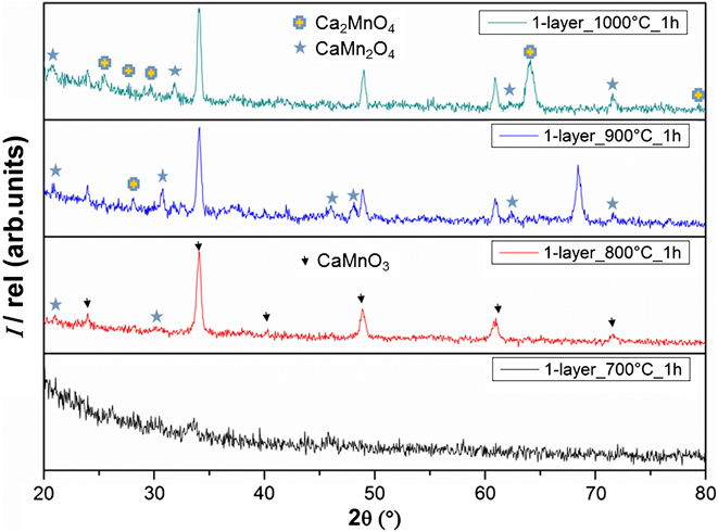
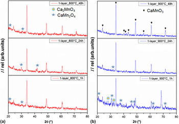
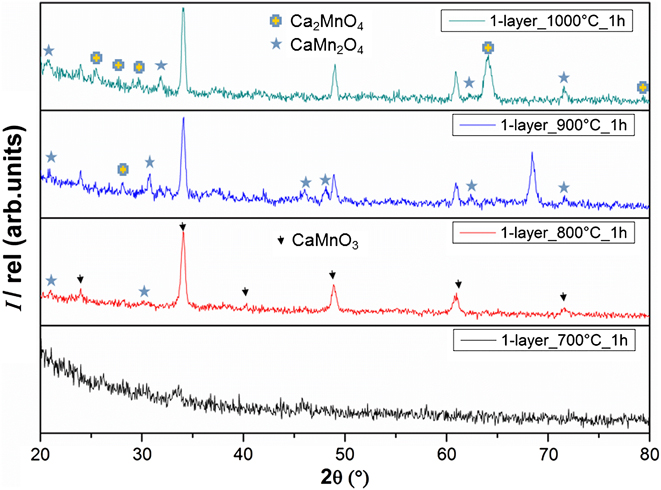
Systematic variations of the synthesis parameters were leading to the definition of the best synthesis conditions to obtain homogeneous, single-phase perovskite-type calcium manganese oxide films on the substrates in a reproducible way. Diffraction patterns of one layer of CaMnO3 films obtained at different annealing temperatures and times are shown in Figs. 1 and 2, respectively. It was found that CaMnO3 films (ICSD Collection Code: 082211) with the desired quality were formed with no discernible secondary phase after heating the film at T = 900 °C for 48 h according to the GIXRD results.Reference Jorge, Dos Santos and Nunes8, Reference Taguchi, Kuniyoshi and Nagao16 Other thermal annealing procedures reveal inclusions of Ruddelsden–Popper phases (Ca2MnO4) and spinel structures (CaMn2O4) in the CaMnO3 main phase, as illustrated in the GIXRD pattern of a sample treated at 800 °C for 48 h (Fig. 2).
Grazing incidence x-ray diffraction (GIXRD) patterns of one-layer CaMnO3 films formed at different annealing temperatures.
GIXRD pattern of one-layer CaMnO3 films formed at (a) 800 °C and (b) 900 °C, respectively, at different annealing times.

The GIXRD patterns at 700 °C in Fig. 1 show no diffraction peak indicating that the phase was not yet crystallized. Thus, it can be concluded that CaMnO3 layer crystallizations were not completed at temperatures below 800 °C even after a reaction time of 24 h (Fig. 2).
In the XRD pattern of Fig. 2, the formation of the crystalline perovskite phase after minimum 1-h thermal annealing can be observed. Depending on the duration of thermal annealing, the appearance of intermediate secondary phases between 1 and 48 h at 800 °C can be observed, indicating that the crystallization process is achieved after 1 h. Longer thermal annealing sequences at elevated temperatures (T = 900 °C) for 24 h lead to a complete crystallization of the perovskite-type film. Further annealing procedures reveal the stability of the film.
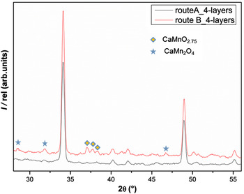
GIXRD analysis of the four layer of films obtained by route A and B is shown in Fig. 3. Both diffraction patterns exhibit reflections corresponding to CaMnO3 (ICSD Collection Code: 082211) as the main phase. The route B pattern contains impurity reflections within the range of 37° ≤ 2θ ≤ 39°, arising from CaMnO2.75Reference Chiang and Poeppelmeier4 and the spinel CaMn2O4 within the range 29° ≤ 2θ ≤ 32.5° and at 47.5° (ICSD Collection Code: 062167).
GIXRD patterns of four-layer films obtained by routes A and B.

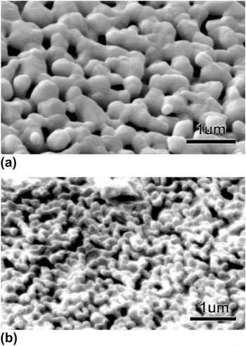
The surface morphology of the films studied by SEM is shown in Fig. 4, where the obtained four layers of film by synthesis route A is displayed in Fig. 4(a) and route B in Fig. 4(b). Both films are not textured, concluding from XRD and electron diffraction data. It is clearly observed that synthesis by route A [Fig. 4(a)] results in a larger grain size than route B [Fig. 4(b)]. This difference in the particle size can be explained due to the variations in the nucleation and growth rate in the different annealing procedures.
Surface morphology of films obtained by (a) route A and (b) route B.

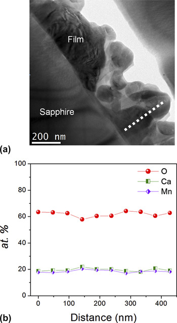
Figure 5(a) shows the TEM bright field (TEM-BF) cross-sectional view of a sample obtained by route A. The particle size ranges from 100 to 400 nm, and the film total thickness is 450–600 nm. The EDS line-scan analysis along the film profile was carried out as it was marked in Fig. 5(a) by the dotted line. The results are displayed in Fig. 5(b) and show a homogeneous CaMnO3 composition along the profile.
(a) Transmission electron microscopy in bright field (TEM-BF) image of the film cross section obtained by synthesis route A with the distinguishable grains; (b) electron dispersion x-ray spectroscopy (EDS) compositional analysis along the film profile marked in (a).

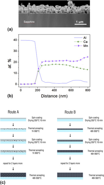
Figure 6(a) shows a dark field STEM (STEM-DF) cross section image of a four-layer film obtained by route B. The grains are smaller than 200 nm, and the thickness ranges from 600 to 700 nm. The EDS cationic composition analysis in Fig. 6(b) shows a Ca deficiency and slight Mn excess in the midsection of the film and the difference increases towards the surface [0.62 ≤ (Ca/Mn) ≤ 0.87]. This Mn excess confirms the enrichment of spinel phase at the surface of the grains.
(a) Scanning transmission electron microscopy in dark field (STEM-DF) cross-section image obtained by synthesis route B with distinguishable grains; (b) EDS compositional analysis along the film profile marked in (a). (c) Graphical description of differences between synthetic route A and B.

The sintering and complete crystallization of the films is achieved when they are treated at 900 °C (Fig. 1). Therefore, in route A each layer is treated at 900 °C for 1 h initiating the nucleation process, but the short time of the thermal annealing does not allow the complete crystallization of the deposited material. The result is a matrix composed of a few CaMnO3 nucleation sites and not yet crystallized material. Every deposited layer provides more precursor material for the nucleation, and the final grain growth is achieved after the four deposited layers with a 48-h final thermal annealing.
In the synthetic route B, the 48-h thermal annealing at 900 °C is performed for every deposited layer. This treatment yields the formation of many nuclei followed by a grain growth until the available material of one deposition is completely consumed. As a result, the final grain size is smaller in route B than route A. It was also observed by XRD in Fig. 3 that samples synthesized by route B contain some impurities of the spinel phase CaMn2O4. These impurities are localized at the surface of the nanocrystals as it is shown in Fig. 6(b). Figure 6(c) shows the difference of the crystallization processes in route A and route B.
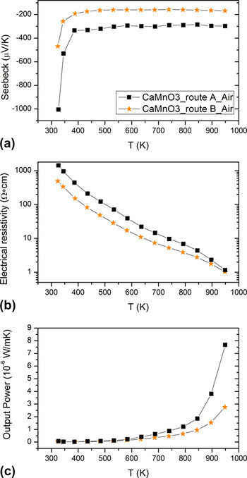
The thermoelectric properties of four-layer films synthesized by routes A and B are shown in Fig. 7. Both films synthesized by routes A and B have reproducible results in heating and cooling curves. The Seebeck coefficient [Fig. 7(a)] is negative in both cases indicating n-type conduction and the values are comparable with bulk samples of the same composition. The electrical resistivity [Fig. 7(b)] reveals a semiconducting behavior and higher values for samples prepared by route A. At 1000 K, the electrical resistivities are 0.60 and 0.48 Ω·cm for routes A and B, respectively.
Temperature dependence of the (a) Seebeck coefficient, (b) resistivity, and (c) power factor for films prepared by synthesis routes A and B, respectively.

The differences in Seebeck coefficient and resistivity are mainly due to the slight nonstoichiometry of the films prepared by route B. The nonstoichiometry of the films is accumulated at the surface of the crystallized films in every layer. The presence of a brownmillerite-type CaMnO2.75 phaseReference Chiang and Poeppelmeier4 detected by GIRXD (Fig. 3) could be the origin of the resistivity and Seebeck value reduction. Oxygen deficiency in manganates generates a mixed Mn(IV)/Mn(III) valence responsible for the high electronic conductivity.Reference Tichy and Goodenough17 The highest power factor was found at 950 K for films obtained by synthesis route A (8.510−6 W/m·K2). This value is slightly better than bulk CaMnO3 (6.25 ×10⁻⁶ W/m·K).Reference Flahaut, Mihara, Funahashi, Nabeshima, Lee, Ohta and Koumoto18
IV. CONCLUSIONS
Polycrystalline CaMnO3 thin films were successfully deposited on sapphire substrates by soft chemistry methods with two different thermal annealing procedures referred as route A and route B. The thermal annealing was done on four layers of deposited films for both routes. In route A, prior final thermal annealing at 900 °C for 48 h, each layer was dried in the furnace at 350 °C for 10 min and treated at 900 °C for 1 h. While in route B, each layer was directly annealed at 900 °C for 48 h after drying at 350 °C for 10 min in the furnace. All films synthesized by these routes are porous with well-interconnected grains. According to GIXRD measurements, route A-films have no discernible secondary phase and showed a higher power factor than route B-films and bulk CaMnO3. The CaMnO3 films exhibit n-type semiconductor behavior and nearly constant Seebeck coefficients at temperatures above 400 K.
ACKNOWLEDGMENT
The Swiss Federal Office of Energy (BfE) and Empa are gratefully acknowledged for financial support.