Introduction
Commercialization of a revolutionary new material can take decades, so much patience and persistence is needed.Reference Boren, Chan and Musso1 When the material is first discovered, there is tremendous hype, which leads to enormous expectations and stimulates plentiful funding for basic research and applications development. This, in turn, leads to initial technology advances that build even more excitement. However, within about a decade, “commercialization anxiety” starts to set in: The quality is not consistent enough. Large-scale production has not been established. High production costs mean that the material is not affordable. Materials suppliers are hesitant to make the large investments required to address quality, scalability, and affordability issues without clear validation of demand for the material. Uncertainties about the intellectual-property landscape and concerns about environmental health and safety add to the perceived risk. As a result, suppliers face even greater difficulties raising the capital needed to address the materials-supply concerns, further extending the commercialization timeline. Such delays and uncertainty are perfectly normal.
History teaches that, for commercialization to succeed, decades can be required for suppliers to become good enough at manufacturing a material and for early adopters to become comfortable enough with using the material in their next-generation products. Carbon fiber has been described as the macroscopic analogue of single-walled carbon nanotubes (SWCNTs).Reference Boren, Chan and Musso1 Its widespread adoption, particularly in the form of epoxy composites, is now considered a commercialization success,Reference Boren, Chan and Musso1 but it took more than two decades for this to happen. It has been two decades since the hype started for SWCNTs, and these materials are just now being commercialized for electronics applications. The good news is that enough progress has been made toward addressing commercialization barriers that it is no longer a question of if commercialization will occur, but just a question of when. Moreover, although certain electronics applications have been proposed for SWCNTs, which application will be the first is still to be determined. The purpose of this article is to highlight key issues affecting the commercialization of carbon nanotube technology, which could be illustrative of some of the types of problems that graphene commercialization might face. Currently, graphene oxide and graphene flakes are available commercially, but at this stage, they are analogous to low-quality traditional multiwalled carbon nanotubes. As yet, there is no commercial production of high-quality graphene films, the equivalent of SWCNTs.
SWCNT production
One of the most significant commercialization barriers for the use of SWCNTs in electronics applications has been the inability of SWCNT producers to meet the high quality standards required for electronics-grade materials at a commercial scale and affordable prices. Some of the more important quality parameters to control for electronics applications are as follows:
• Chirality is defined by the nanotube diameter and the orientation of atoms in the single atomic layer of carbon that constitutes the nanotube. Chirality determines whether the nanotube has metallic or semiconducting electronic properties and, if semiconducting, the size of the bandgap.
• Purity defines how much of the product is actually SWCNTs rather than other forms of carbon (amorphous carbon, multiwalled carbon nanotubes, carbon nanofibers, etc.) and non-carbon species (metals, metal carbides, metal oxides, etc.). Typically, the non-carbonaceous impurities are quantified by determining the residual mass content after heating a sample to a temperature in the range of 650°C, often using thermogravimetric analysis (TGA). Purity with respect to the percentage of carbon that consists of SWCNTs is known as “relative purity” and is estimated from electron micrographs or in some cases by TGA.Reference Jansen and Wallis2 These impurities can compromise the performance and yield of electronic devices.
• Defects exhibit sp Reference Chamness3 hybridization instead of the preferred sp Reference Jansen and Wallis2 hybridization and define the structural integrity of the nanotube. Defects can compromise the electron-transport properties of nanotubes. Defects can also increase nanotube breakage during dispersion processes (such as ultrasonication), which can compromise nanotube length. Longer tubes are generally more desirable for forming nanotube networks with good electron-transport properties at low areal densities.
SWCNTs also need to be affordable for applications. Most electronics applications utilize thin films of SWCNTs (on the order of 10 nm in thickness, with areal densities on the order of 10 mg/m2). The cost of these thin films is currently on the order of US$10/m2. Over time, competitive pressures and economies of scale will likely drive this price down to US$1/m2or less. Assuming that the SWCNT material cost is ~50% of the thin-film value, this means that SWCNT commercial pricing needs to be less than US$500/g today and less than US$50/g in the future for commercial viability.
Finally, these key quality and cost parameters must be met using a scalable production method that is capable of delivering commercial quantities with efficient utilization of labor and capital. For electronics applications, the annual production of SWCNT thin films could be on the order of 100 million m2 per year, growing to over 1 billion m2 per year.Reference Chamness3 This means that the SWCNT supply chain must be capable of delivering on the order of 1–10 tonnes per year. To the extent that graphene technology is directed toward similar markets, these caveats about quality, scale, and price will also apply.
Commercial production processes
Currently, multiple approaches are employed for the fabrication of high-quality graphene materials, as discussed in the articles in this issue by Nyakiti et al., Bartelt and McCarty, and Jaber-Ansari and Hersam. Likewise, multiple methods can be used for the fabrication of SWCNTs, each providing SWCNTs with characteristic structures and compositions. For commercial SWCNT production, arc discharge, laser ablation, and two types of catalytic chemical vapor deposition (CCVD) are the main processes that have been used.
Arc discharge and laser vaporization
Arc dischargeReference Bethune, Kiang, De Vries, Gorman, Savoy, Vazquez and Beyers4 and laser ablationReference Thess, Lee, Nikolaev, Dai, Petit, Robert, Xu, Lee, Kim, Rinzler, Colbert, Scuseria, Tomanek, Fischer and Smalley5 were the first methods employed to synthesize SWCNTs on the scale of tens of grams. Both of these methods involve evaporation of solid carbon in the presence of a mixed transition-metal catalyst, such as nickel/cobalt or nickel/yttrium, followed by condensation of gaseous carbon atoms into a sootlike material that, in addition to CNTs, contains other forms of amorphous and graphitic carbon. These methods generally yield materials with diameters in the range of 1.3–1.8 nm. The relative purity (percentage of carbon in SWCNTs) of the material from the reactor is typically less than 35%, and extensive purification is required to isolate the SWCNTs. This process often involves refluxing the “soot” in nitric acid (typically ~3 M) to remove catalyst metals and amorphous carbon and then applying a series of aqueous extractions at gradually increasing pH to isolate and remove the different forms of carbon.Reference Hu, Yu, Kim, Zhao, Itkis, Bekyarova and Haddon6 Final yields can be as low as 10% of the carbonaceous material produced. The high reaction temperature used is believed to produce SWCNTs with low defect concentrations compared with most other methods. Thus, the electron-transport properties of isolated SWCNTs made from arc or laser methods can be superior to those of SWCNTs produced by other methods. However, the high cost of isolating the SWCNTs to obtain material pure enough for electronics applications renders these methods very expensive, often as high as US$100/mg when sold in the form of electronics-grade ink.7 Furthermore, these methods have not demonstrated the capability of controlling chirality, essential for many electronics applications.
Catalytic chemical vapor deposition (CCVD)
The CCVD method involves the decomposition of a carbon feedstock catalyzed at the surface of metallic nanoparticles, which also act as nucleation sites for the growth of carbon nanotubes. CCVD is versatile in the sense that it offers the ability to utilize a number of different carbon sources (carbon monoxide, hydrocarbons, alcohols, aromatics, etc.) with varying catalyst formulations and reactor designs, as well as wide-ranging temperatures and pressures. The two most popular CCVD processes used commercially today are the floating-catalystReference Nikolaev, Bronikowski, Bradley, Rohmund, Colbert, Smith and Smalley8 and supported-catalystReference Kitiyanan, Alvarez, Harwell and Resasco9 methods.
Floating-catalyst CCVD
The floating-catalyst method,Reference Nikolaev, Bronikowski, Bradley, Rohmund, Colbert, Smith and Smalley8 which utilizes a gaseous catalyst, typically involves the decomposition of organometallic precursors at high temperatures to generate metallic nanoparticles in situ. In the case of the high-pressure carbon monoxide (HiPco) process (originally commercialized by Carbon Nanotechnologies, Inc.), CO serves as the carbon source, and iron pentacarbonyl [Fe(CO)5] is the metallic precursor. Typical temperatures between 800°C and 1200°C and pressures of up to 50 atmReference Nikolaev, Bronikowski, Bradley, Rohmund, Colbert, Smith and Smalley8, Reference Bronikowski, Willis, Colbert, Smith and Smalley10 make the HiPco process difficult to scale, and commercial quantities of SWCNTs are no longer being made by this process. Thomas Swan, a fine-chemicals manufacturer in the United Kingdom, has successfully scaled up the production of SWCNTs using the floating-catalyst method to kilograms per day. Its process does not require high pressure, so capital efficiency is much better than for the HiPco process.
However, control of diameter and chirality is extremely difficult with the floating-catalyst method because of the inability to control metal particle sizes precisely at the nanoscale prior to SWCNT nucleation and growth.Reference Moisala, Nasibulin and Kauppinen11, Reference Bachilo, Strano, Kittrell, Hauge, Smalley and Weisman12 SWCNTs synthesized from floating catalysts also tend to include large amounts of other forms of carbon, because the growth mechanism requires rigorous control of carbon segregation or diffusion on the metal nanoparticle surface.Reference Bronikowski, Willis, Colbert, Smith and Smalley10 When carbon surface diffusion occurs, it is expected that the catalyst particle becomes encapsulated by nontubular carbon. Thus, even though the floating-catalyst synthesis method is more scalable than the laser and arc-discharge methods, it still has the limitations of no chirality control (two-thirds of SWCNTs are semiconducting) and low relative purity (which can be below 50%). Thus, the needs for extensive purification, similar to that described for laser- and arc-produced materials, and nonscalable chiral separation methods to meet quality requirements make the floating-catalyst method very expensive for electronics applications of SWCNTs.
Supported-catalyst CCVD
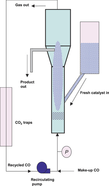
Supported-catalyst CCVDReference Kitiyanan, Alvarez, Harwell and Resasco9 combined with fluidized-bed reactor technology, shown schematically in Figure 1, has enabled SWCNTs to be made at a commercial scale with high purity and chirality control. This method, also known as the CoMoCAT® process, was invented by the Resasco groupReference Bachilo, Balzano, Herrera, Pompeo, Resasco and Weisman13 at the University of Oklahoma and subsequently scaled up and commercialized by SouthWest NanoTechnologies, Inc. (SWeNT). This process utilizes proprietary catalysts based on cobalt and molybdenum (and other transition metals) supported on silica particles. Fluidized-bed reactors are inherently scalable (labor- and capital-efficient) and enable precise control of temperature and gas composition throughout the entire reaction zone (because of uniform heat and mass transfer resulting from fluidization).
Schematic of a fluidized-bed reactor for manufacturing single-walled carbon nanotubes by the CoMoCAT process. This design exhibits extremely good temperature uniformity and is easily scalable.

The combination of precise control of catalyst sites and precise control of reactor conditions enables the production of SWCNTs having controlled diameters and chirality distributions.Reference Bachilo, Strano, Kittrell, Hauge, Smalley and Weisman12 Metal or quartz reactors can be used because the growth temperature is typically below 900°C and the process is capable of operating at atmospheric to moderate pressures.
With the CoMoCAT process, the properties of the SWCNT product can be modified by varying the reaction temperature,Reference Naumov, Kuznetsov, Harutyunyan, Green, Hersam, Resasco, Nikolaev and Weisman14 the gaseous carbon feed source and partial pressure, and the type of catalyst support and/or metal composition. Through appropriate selection of these growth parameters, SWeNT successfully developed and introduced commercially a new SWCNT material, SG65i, that has an average tube diameter of 0.77 ± 0.02 nm, over 40% (6,5) chirality, and 95–97% semiconducting chiralities. Carbon purity after digestion of the catalyst is typically greater than 95 wt%, and relative purity is typically ~99%, which means that the SWCNT purity is ~94 wt%. This is a higher purity than obtained by other SWCNT commercial production methods but still lower than the 99.9 wt% purity target for the more demanding electronics applications.
A limitation of supported-catalyst CCVD is that the catalyst support represents a high percentage of the mass of the as-produced SWCNT products but there are practical limits to the efficiency of digesting the supported catalyst. (The practical limit for SWCNT purity is ~99 wt%.) SWeNT is currently addressing this technical challenge by pursuing the development of nanotube harvesting methods to release the SWCNTs from the supported catalyst and subsequently recycle the catalyst. This method is expected to increase SWCNT purity to over 99.9 wt% without compromising any of the other key quality parameters (which are largely controlled by the synthesis process). By recycling process gases and catalyst and eliminating purification and waste-treatment operations, SWeNT expects to realize a production cost of much less than US$10/g (and most likely less than US$1/g) when mass-production quantities are required.
Graphene production
In terms of fabrication, the situations for graphene and SWCNTs are similar. There are many different types of “graphene” materials, produced by very different methods. Two examples are graphene oxide (GO) nanoplatelets produced by exfoliation of graphiteReference Blake, Brimicombe, Nair, Booth, Jiang, Schedin, Ponomarenko, Morozov, Gleeson, Hill, Geim and Novoselov15 and continuous thin films of graphene produced by catalytic CVD synthesisReference Li, Cai, An, Kim, Nah and Yang16 (with copper as a commonly used catalyst). GO nanoplatelets are viewed as being affordable and made from a scalable process,Reference Allen, Tung and Kaner17 but their quality, in terms of control of structure, purity, and defects, is a major concern (especially for electronics applications). This is analogous to traditional multiwalled CNTs, which are affordable and made from a scalable process but do not meet the quality requirements for electronics applications.
CVD-grown graphene materials are generally viewed as being higher in quality than GO nanoplatelets, but there are significant questions about scaling CVD growth to large areas. Most CVD-grown graphene is produced at the wafer scale at high cost. Additionally, the continuous film is heterogeneous, exhibiting patches of high-quality graphene surrounded by grain boundaries. These patches are rather small in size (≪1 mm). This quality, cost, and availability tradeoff is analogous to that for single-walled CNTs, which have historically been made at high cost and small scale and lacked the chirality control and purity needed for electronics applications.
Also, similarly to CNTs, graphene materials are difficult to characterize, which makes it more challenging to improve quality—one can purposefully improve only what one can measure. There is no doubt that the significant gains in CNT quality achieved during the past decade have resulted from advances in metrology. A key question for graphene applications will be how long it will take to characterize graphene structure and properties, as well as understand and precisely control the fabrication of graphene and its precursor materials.
Graphene that is grown epitaxially on SiC is an exception to the preceding discussion (see the articles in this issue by Nyakiti et al. and Ruan et al.). Such epitaxial graphene can be patterned and used on the original substrate without the transfer required for nanotubes and for graphene synthesized by other means. In addition, the high quality of the epitaxial graphene that can be obtained makes it suitable for sophisticated characterization, as discussed in the articles in this issue by Hicks and Conrad and Wong et al.
Electronics applications
We now consider SWCNTs produced at the commercial scale and examine the implications for electronics applications of graphene in thin-film transistors and transparent conductive films.
Thin-film transistors
One of the most exciting commercialization opportunities for SWCNTs is as a semiconducting thin-film material for transistors. It is estimated that the overall market for semiconducting materials was nearly US$48 billion in 2011,Reference Chamness3 with single-crystal silicon (SCS), which is not printable, dwarfing printed semiconducting materials. The increasing demand for lower-cost printed electronics will drive rapid growth in the market share of printable semiconducting materials.
Alternative materials to replace SCS are being aggressively pursued to address unmet market needs for semiconducting materials with printability, flexibility, low-temperature processability, and lower cost. Printed or printable semiconductor materials are expected to exceed US$9 billion in 2012, growing to more than US$63 billion in 2022, with the leading applications being OLED displays, photovoltaics, and other display technologies such as those using electrophoretic and electrochromic technologies.18
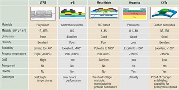
The strengths and weaknesses of the major alternatives to SCS were outlined in a report by NPD DisplaySearch19 and are summarized in Table I. Although TFT devices have been demonstrated using all of these materials, only SWCNTs are positioned to meet all of the requirements of performance and cost. For example, printability is problematic for low-temperature polysilicon (LTPS), amorphous silicon (a-Si), and metal oxides because their deposition requires high temperatures (200–350°C), which limits the range of other materials that can be employed as substrates and insulating layers. Moreover, pentacene has significant issues of stability, and devices made using this material have demonstrated low mobility.
Strengths and weaknesses of the major alternatives to single-crystal silicon for thin-film transistors.

a-Si, amorphous silicon; CNT, carbon nanotube; LTPS, low-temperature polysilicon. Chart courtesy of Kosmas Galatsis, Aneeve Nanotechnologies.
The required properties of SWCNTs for use in TFT devices have been extensively reviewed.Reference Rouhi, Jain and Burke20–Reference Cao and Rogers22 As mentioned earlier, certain chiralities of SWCNTs are semiconducting in nature, in fact having extraordinary semiconducting performance. In a TFT, for example, the semiconducting material should create a very low-resistance path in the on state, yet have very high resistance and low current leakage when switched off. Semiconducting SWCNTs exhibit quasiballistic conduction (that is, very nearly zero resistance), and in the off state, assuming that no conductive species are present, they present a very high resistance to current flow. To improve the performance of SWCNT TFTs, as measured by high mobility (>10 cm2 V−1 s−1) and high on/off ratio (>106), Rouhi et al.Reference Rouhi, Jain and Burke20 showed that the key requirements are increasing purity, with respect to both semiconducting-to-metallic ratio (>99%) and residual metallic impurities, and maximizing SWCNT length. Minimizing tube diameter also increases mobility.Reference Asada, Nihey and Ohmori23
TFTs present an attractive market opportunity for all SWCNT suppliers, and each is addressing the challenge of meeting material requirements in its own fashion. To address these issues, SWeNT is capitalizing on the unique capability of the CoMoCAT process described earlier. The capability to control chirality allows synthesis of materials with very high concentrations of semiconducting species in the as-synthesized material (currently 95–97% for recently introduced grades), and further optimization of synthesis control is expected to result in ~99% semiconducting CNT species at a commercial scale (kilograms per day) and affordable pricing (~US$200/g).
Another element crucial to commercialization is printability. The ultimate manifestation of printable electronics is the roll-to-roll coating and printing of each layer in the semiconductor device. Materials with low drying/curing temperatures are available for insulators and electrodes, but only SWCNTs and pentacene are easily printed, and pentacene must overcome challenges of low mobility and environmental stability.
Finally, accelerated commercialization will require partnerships. Notably, SWeNT, Chasm Technologies, and Panasonic have teamed up in a grant program from the state of Oklahoma to develop tailored SWCNTs and processes for printing TFT backplanes for OLED televisions (TVs). Successful development will have the effect of enabling OLED TVs, which offer many advantages over other TV technologies (improved color, wider viewing angles, faster video response, thinner profile, and lower energy consumption) but suffer from high cost compared with the more mature LCD TV technology. A printed TFT backplane would help offset some of this cost disadvantage. SWeNT is also working closely with other industrial and university partners developing their own proprietary methods of building devices based on SWCNT semiconducting materials.
In the longer term, the impact of the development of highly purified semiconducting SWCNTs will be profound. It is widely recognized that Moore’s law cannot be supported indefinitely by silicon-based technology. The leading candidates for replacing silicon are SWCNTs and, to a lesser extent, graphene nanoribbons. There are few, if any, known alternatives. New manufacturing processes will be needed to carefully position individual semiconducting SWCNTs (this capability has been demonstrated on a laboratory scaleReference Avouris24), and much higher purity levels will be needed (99.9999% semiconducting species), but the market forces driving this development will be overwhelming.
It is important to note that using SWCNTs for digital devices is not a new idea. In fact, in 2006, Nantero developed its unique SWCNT-based NRAM™ (nano-random-access memory) technology,Reference Smith, Rueckes, Konsek, Ward, Brock and Segal25 which has been commercialized and is currently deployed in aerospace applications by Nantero licensee Lockheed Martin. For these applications, it is important that these devices be “radiation hardened”, be considerably faster and denser than dynamic random-access memory (DRAM), have substantially lower power consumption than DRAM or flash memory, and be as portable as flash memory. For this application, conducting, not semiconducting, SWCNTs are required. However, very high SWCNT purity is essential (>99.9%), which is currently achievable only by extensive and therefore expensive purification processes. The development of high-purity semiconducting SWCNTs for TFTs (through controlled synthesis versus nonscalable separation methods) should also be applicable to conducting SWCNTs for NRAM. This could help extend the use of NRAM beyond aerospace applications.
Transparent conductive films
Transparent conductive films (TCFs) are used in a wide range of products, including liquid-crystal displays (LCDs), e-Readers, organic light-emitting diode (OLED) and quantum-dot light-emitting diode (QDLED) displays and lighting, touch sensors, photovoltaic modules, and architectural windows. Sputtered indium tin oxide (ITO) dominates the market, primarily because of its excellent optoelectronic performance (transparency, conductivity, haze, color, stability), although several other sputtered metal oxides have recently been introduced as less-expensive substitutes. However, device manufacturers are seeking TCF materials with improved optoelectronic performance, new features (printability, flexibility, stretchability, low-temperature processing), abundant supply, and lower cost. ITO and its alternatives fall into four broad categories:
• transparent conducting oxides (TCOs), including ITO;
• metal-based systems, such as silver grids or silver nanowires;
• conductive polymers, such as polythiophenes, including poly(3,4-ethylenedioxythiophene) (PEDOT); and
• carbon nanotubes (CNTs), especially single- and few-walled CNTs.Reference Choi, Lahiri, Seelaboyina and Kang26
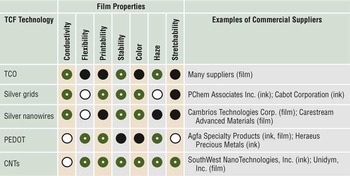
It is apparent from Table II that TCO materials are not suitable for electronics applications requiring printability, flexibility, or stretchability. This creates a significant opportunity for alternative TCF materials. In addition, both silver grids and silver nanowires offer superior electrical conductivity compared with ITO, which is highly desirable for projected capacitive multitouch sensors used in tablet computers and smart phones. As a result, silver grids and silver nanowires are taking share away from ITO. Silver grids and silver nanowires are also more flexible than ITO, but they are not stretchable, and they are much less flexible than PEDOT or CNTs. One major limitation of silver nanowires is that they are not available as printable ink, whereas silver grids can be printed. Much lower cost can be achieved with printing, where material is placed only where it is needed, whereas with sputtered ITO film, extensive masking and etching processes are required.
Strengths and weaknesses of transparent conductive film (TCF) technologies.

 Excellent,
 Good,
 Poor.
CNT, carbon nanotube; PEDOT, poly(3,4-ethylenedioxythiophene); TCO, transparent conducting oxide.
PEDOT is less conductive than ITO, but its conductivity is still adequate for a wide range of applications. PEDOT is also printable, flexible, and stretchable. This is why PEDOT has taken share from ITO. Two major limitations of PEDOT, however, are its blue color and concerns about its environmental stability (drift in conductivity after temperature/humidity cycling). Note that ITO also has a color limitation (yellow). Any color in the film must be compensated by the use of color-correcting filters. The neutral color of SWCNTs negates the need for such filters.Reference Hecht, Thomas, Hu, Ladous, Lam, Park, Irvin and Drzaic27
CNTs can have conductivity similar to that of PEDOT, which is the prime competition for CNTs in TCF applications. CNTs are printable and even more flexible and stretchable than PEDOT. The main advantages of CNTs compared with PEDOT include neutral color and better environmental stability. The most significant disadvantage of CNTs relative to PEDOT is that device designers are more hesitant to use the much newer TCF material. This will change over time, as more device companies adopt CNT TCFs. Also, over time, as production costs continue to drop for CNT materials, it is expected that TCFs manufactured from CNTs will be considerably less expensive than those manufactured from all of the other materials listed in Table I.
CNT TCF applications
In the near term, CNTs are expected to see commercial success in four TCF application areas: e-Readers, electrochromic windows, low-end resistive touch sensors,Reference Hecht, Thomas, Hu, Ladous, Lam, Park, Irvin and Drzaic27 and stretchable touch sensors.Reference Feng, Liu, Wu, Liu, Cheng, Zhang, Sun, Li, Fan and Jiang28, Reference Jeong, Choi, Lim and Lee29 CNT TCFs can meet the optoelectronic requirements for each of these applications as follows:
In the case of e-Readers, the transparent electrode does not require the sheet resistance (R s) to be as low as that of ITO. In fact, values of a few kiloohms per square are acceptable or even desired for the electrophoretic display technology. However, because most e-Readers are reflective displays, very high visible-light transparency (VLT) is required for the TCF (VLT ≈ 99%).
In contrast, electrochromic windows require much lower sheet resistance (~100 Ω/sq), but can tolerate or prefer lower VLT (~75%). In both cases, neutral color, very low cost, and environmental stability are also important.
Resistive touch sensors for low-end LCDs, for which rapid response is not necessary, require R s values in the range of 300–500 Ω/sq and VLT of 90–95%. Unidym has demonstrated that its CNT TCF films can reach these targets.Reference Feng, Liu, Wu, Liu, Cheng, Zhang, Sun, Li, Fan and Jiang28 Unidym has also done considerable work in addressing technical challenges associated with resistive touch sensors, which are more demanding in terms of electromechanical and environmental stability than projected capacitive touch sensors.
Stretchable touch sensors are an emerging market opportunity for CNT TCFs, especially in the area of printable, stretchable sensors, where projected capacitive touch sensors are printed on flexible plastic film, laminated to form a multilayer film subassembly, and then stretched over a mandrel to form a three-dimensional shape. This concept has been demonstrated using both PEDOT and CNT TCFs, but CNTs are expected to gain share because of their neutral color, environmental stability, and superior stretchability. Because such three-dimensional touch sensor subassembliesReference Feng, Liu, Wu, Liu, Cheng, Zhang, Sun, Li, Fan and Jiang28, Reference Jeong, Choi, Lim and Lee29 are less expensive than current technology, they are expected to replace traditional buttons, sliders, membrane switches, and so on in applications such as automobile interiors, consumer appliances, medical devices, and office equipment. Such sensors also provide a more reliable and more aesthetically pleasing user interface for consumers. This application also has modest sheet resistance and VLT requirements, with R s≈ 1000 Ω/sq and VLT ≈ 85% generally being acceptable.
For applications requiring conductivity higher than that of ITO (R s≈ 10 Ω/sq) and fairly high VLT (~95%), printed silver grids combined with either printed PEDOT or CNT TCFs with very high VLT (~99%) provide an interesting hybrid approach. One potential application of this approach is organic photovoltaic (OPV) modules, which can use a charge distribution layer on top of the silver grid.
CNT TCF business model
Companies aiming to commercialize CNT TCFs have adopted different strategies, marketing either finished films30 or printable inks.7 Unidym’s business model includes selling CNT-coated poly(ethylene terephthalate) (PET) films (based on mainly few-walled CNTs). This approach positions Unidym’s film products as direct replacements for ITO- or PEDOT-coated PET films, which is convenient. Toray Industries has also commercialized a CNT-coated PET film product (based on double-walled CNTs).
If patterning is required, then Unidym recommends laser ablation to selectively remove regions of the CNT film. This approach technically works very well, but most fabricators do not have the required laser tool and might be hesitant to make the capital investment (even though it is less than US$100,000). In contrast, ITO and PEDOT films can be etched using standard wet-etch approaches. If a patterning process that is compatible with existing wet-etching equipment can be developed for CNT films, then a significant barrier to adoption would be removed. For applications that do not require patterning, this is not an issue; however, most TCF applications do require some degree of patterning.
SWeNT’s business model is different and involves selling CNT inks based on SWCNTs. (Note that the term “ink” is used interchangeably for coating fluids and printable inks.) This approach makes SWeNT’s CNT ink products a direct replacement for PEDOT inks, the leading material for use in printable TCFs. SWeNT also sells CNT materials (in the form of powders, press cakes, pastes, and dispersions) to other companies, so that they can make their own CNT inks. For example, Brewer Science, Inc., makes its own CNT inks for electronic applications using SWCNT materials from SWeNT and other suppliers. The most popular printing techniques for TCFs are screen printing (low to intermediate volumes) and flexographic printing (high volumes). The most popular coating techniques for TCFs are slot-die, gravure, and spray coating. Printing techniques such as ink jet and aerosol jet are also used for TCFs, but mainly for prototyping.
Clearly, whether the final CNT TCF products are films (e.g., Unidym, Toray) or inks (e.g., SWeNT, Brewer Science), it is essential to have a method for converting CNT raw materials into inks that are compatible with industrial printing and coating equipment. This is not a trivial undertaking, as we now discuss.
CNT inks
The conversion of CNTs into useful inks or coating fluids is highly dependent on the application method and the final product. To produce a film of conductive CNTs, the manufactured CNTs must be converted from bulk dry form into a fluid that can be applied using one of several printing or coating techniques. For example, for screen printing, the CNTs need to be formulated into a fluid that has the correct rheological and wetting properties, that is, generally high viscosity with carefully designed shear-response characteristics. For slot-die coating, to create a uniform CNT layer over a wide area, the goal would be a more Newtonian fluid with excellent spreading characteristics. In each case, it is necessary to disperse the original CNT bundles that tend to form in SWCNT dispersions through agglomeration resulting from van der Waals attractions. Reducing bundle diameter, exposing individual tubes as much as practical, and maintaining separation throughout the printing/coating and drying process results in better performance.
The CNT dispersion process can be tricky, requiring high energy (e.g., sonication) to reduce the nanotube bundle diameter and disperse individual nanotubes. It also requires functionalization of the CNT surfaces (either covalently or noncovalently) to ensure that dispersion is maintained in the final ink. Excessive dispersion energy can shorten the nanotubes, thereby degrading performance.Reference Wu, Chen, Du, Logan, Sippel, Nikolou, Kamaras, Reynolds, Tanner, Hebard and Rinzler31 This situation is exacerbated if the initial CNTs already contain defects. Commercially available CNTs often contain impurities (residual catalyst, other forms of carbon), and the elimination of these materials can be an important step in the creation of a high-quality ink. It is essential that CNT suppliers improve quality (chirality, purity, defects) to eliminate the need for expensive, nonscalable purification and chirality-separation methods and to enable a reasonable process window for the dispersion step in the ink-making process.
Evolution of CNT TCFs
One of the early pioneers in the development of CNT TCFs, Eikos, Inc., reported excellent optoelectronic performance in 2005, with VLT in the range of 90–97% and R s values in the range of 200–500 Ω/sq.Reference Trottier, Glatkowski, Wallis and Luo32 The CNTs used in that work were reported to be SWCNTs made by arc discharge. Other work by Eikos also involved the use of SWCNTs made using laser vaporization. Extensive purification processing was done to separate the SWCNTs from amorphous carbon, metal catalyst, and other contaminants, and then SWCNT thin films were spray-coated onto various substrates, including PET and glass.
This early work was encouraging in that the commercial requirements for several applications could be met with the resulting CNT TCF coating. However, the low SWCNT purity resulting from the laser or arc-discharge synthesis methods required complex purification processes, thus limiting scale and increasing cost. Furthermore, the spray process was not widely accepted for reasons of cost (low productivity) and environmental health and safety concerns related to airborne CNTs. It is interesting to note that Eikos’ CNT inks did not require the use of surfactants. Despite limited commercial success, Eikos made important technology advances in areas such as improving the R sstability of CNT TCFs and applications development (e.g., touch sensors, LCD color filters, aerospace transparencies).
In 2008, Unidym reported few-walled CNTs produced by a supported-catalyst CCVD process with performance equivalent to or better than that of SWCNTs produced by the laser or arc-discharge methods.Reference Park, Hu, Gruner, Irvin and Drzaic33 The CNTs were converted to an aqueous ink, and CNT-coated PET films were produced using a roll-to-roll coating machine configured with an in-line rinsing/drying module to extract the surfactant from the CNT film. Although this ink did include surfactants, Unidym and othersReference Wu, Chen, Du, Logan, Sippel, Nikolou, Kamaras, Reynolds, Tanner, Hebard and Rinzler31, Reference Geng, Kim, So, Lee, Chang and Lee34 reported that use of nitric acid in the rinsing tank rendered extraction of surfactant more effective and allowed the CNTs to be doped at the same time (both of these factors enhance optoelectronic performance). Unidym demonstrated CNT-coated films at the Society for Information Display (SID) Display Week conference in 2008Reference Hecht, Thomas, Hu, Ladous, Lam, Park, Irvin and Drzaic27 as both film samples and films incorporated into devices (touch sensors, e-Readers). This was an important demonstration to the displays industry that CNT TCFs were well on their way toward commercialization.
By 2008, it had become apparent that CNT inks have a limited operating window as a result of their inherent material properties. Low-concentration inks (<0.2 mg/ml) had been successfully demonstrated, but inks at such concentrations require high wet coverage to reach the targeted R s and VLT values.Reference Trottier, Glatkowski, Wallis and Luo32 Low-viscosity inks at high wet coverage can be difficult to dry uniformly, whereas high-viscosity fluids, if achieved by the addition of thickeners, result in high R svalues because of residual thickener. Increasing the CNT concentration would seem an obvious option, but doing so would require surfactants/dispersing agents at fairly high levels (as discussed earlier), and the presence of residual surfactants in the dried CNT layer would also adversely affect the optoelectronic properties. This issue can be addressed by rinsing the final film with water, alcohol, or nitric acid, which can result in a CNT layer having good optoelectronic performance. A practical commercialization issue is that few printing or coating lines are currently set up for an in-line rinsing process and an additional drying station. Also, in the United States, upgrades to the wastewater treatment system would be needed at a large scale, as the US Environmental Protection Agency does not allow CNTs to be discharged.
Recently, SWeNT announced a screen-printable solvent-based CNT ink based on V2V™ (“Viscous-to-Vanishing”) ink technologyReference Arthur and Hurley35 developed by Chasm Technologies. This technology utilizes an ink vehicle that is 100% volatile, leaving only CNTs on the substrate surface after the ink has dried. The ink has rheological properties needed for feature printing with high edge sharpness and small (0.3-mm) feature sizes. The CNT concentration can be up to 1 mg/ml and low-temperature processing (110°C, 230°F) is standard. Results of R s ≈ 1000 Ω/sq at 85% VLT in one printing pass have been achieved. This level of optoelectronic performance is sufficient for the printable/stretchable three-dimensional touch sensor application. The ease and quality of printing by standard industrial printing methods makes this ink easy to insert into existing printing shops. The optoelectronic performance of surfactant-stabilized aqueous inks is currently superior to that of screen-printable V2V inks because of the superior degree of dispersion of the former,36 but this performance gap is expected to narrow over time. For aqueous inks, SWeNT has demonstrated CNT TCF performance (using SWCNTs produced by SWeNT) similar to those reported by EikosReference Trottier, Glatkowski, Wallis and Luo32 and Unidym.Reference Park, Hu, Gruner, Irvin and Drzaic33
Graphene in applications
It is not a surprise that many of the same applications that have been touted for SWCNTs are also being mentioned as possible targets for graphene. Transparent conductors, semiconductor channel materials, sensors, membrane materials, electro-optical devices, and thermal-management layers have all been mentioned as application areas for both SWCNTs and graphene.Reference Wassei and Kaner37 Graphene and SWCNTs have been mentioned as possible components in electronic displays, touch panels, integrated circuits, photovoltaic panels, and others. Many of these application areas for SWCNTs have been mentioned in this article. It is likely that many of the problems and opportunities described for SWCNTs will also be relevant for graphene for practical, large-scale use in these areas.
Graphene materials are not easy to apply in a manufacturing environment—yet. This is one area in which lessons learned from the CNT commercialization experience are directly applicable to the manufacture of graphene. GO nanoplatelets can be coated and printed, and such inks are available for a variety of printing and coating applications. This is good. Unfortunately, the quality of current GO nanoplatelets limits electronics applications. The lack of a scalable and affordable transfer method is a major limitation for CVD-grown graphene. Once this problem is solved, then the greatest limitation will be the issue of the presence of grain boundaries in the copper substrate causing defects in the graphene structure. Of course, making graphene materials easy to use will be easier if the target application area(s) are narrowly defined. For a long time, CNTs were expected to be used for every conceivable application. This actually stunted commercialization. Today, single-walled CNTs are largely being developed for electronics applications, and multiwalled CNTs are largely being developed for applications in conductive polymers. This focus on applications makes product commercialization more feasible. The same clarity and focus must be developed for graphene.
Summary
After two decades of research and development, carbon nanotube (CNT) materials are starting to show significant progress toward commercialization in electronics applications such as transistors and transparent conductive films. This development can be attributed to three key factors: (1) CNT materials of high quality (chirality, purity, defects) are available at the commercial scale with affordable pricing. (2) CNTs are available in easy-to-use product forms such as films and inks. (3) Early adopters in the printed electronics industry are now ready to embrace lower-cost, printable, and flexible/stretchable alternatives to established electronics materials such as ITO and silicon.
These facts provide important lessons for other exciting nanomaterials such as graphene. Commercialization of advanced materials can take decades for suppliers to develop proficiency in making a material with sufficiently high purity and early adopters to become comfortable with using the material in their next-generation devices, so patience and persistence are needed. Not only do materials such as graphene need to solve an existing problem, but they need to solve it better than competitive solutions, and they need to solve it in a reproducible and scalable way. Not only will some of the lessons learned for CNTs be relevant for graphene commercialization, but it is nearly certain that graphene will develop a completely new and unexpected set of challenges as well.
Graphene might well surpass SWCNTs as a transparent conductor, as any graphene material with dimensions greater than 10 nm is inherently metallic in nature.Reference Jiao, Zhang, Wang, Diankov and Dai38 However, SWCNTs might offer an advantage in semiconducting applications because of their bandgap.
There are many similarities between the graphene landscape today and the CNT landscape of 10 years ago. However, it is hoped and expected that the development cycle will be somewhat shorter for graphene, based on the lessons learned for CNT materials.
Acknowledgments
The authors acknowledge Kosmas Galatsis from Aneeve Nanotechnologies for providing the TFT materials landscape information. Also, the authors are grateful for the funding provided by NIST TIP and the Oklahoma Center for the Advancement of Science and Technology (OCAST).