I. INTRODUCTION
Electroless nickel immersion gold plating has been widely used as under bump metallization (UBM) of printed circuit board (PCB) and ball grid array (BGA) because of its selective deposition properties with uniform thickness, good solderability, and corrosion resistance.Reference Mei, Kauffmann, Eslambolchi and Johnson1, Reference Goyal, Lane, Kinzie, Panichas, Chong and Villalobos2 However, formation of Ni3P and Ni3SnP at the solder/UBM interface increased the susceptibility of the solder joints to brittle cracking,Reference Song and Yu3–Reference He, Chen and Qi6 and many efforts were made to improve the solder joint reliability by changing the solder composition.Reference Jee, Yu and Ko7, Reference Li, Mannan, Clode, Whalley and Hutt8 In contrast, less efforts were paid to the modification of the UBM composition.
Electroless NiWP and NiReP films were first made by Pearlstein et al.Reference Pearlstein and Weightman9 by adding salts of W and Re into the electroless nickel bath, which was followed by the codeposition of Mo, Sn, Cu, Fe, Co, Zn, and Mn with electroless nickel.Reference Mallory and Horhn10–Reference Osaka, Kasai, Koiwa and Goto15 These films were used as passivation layers for steels and magnetic materials due to excellent wear/corrosion resistances and magnetic properties. Attempts to use NiWP film as UBM of microelectronics packaging were made by Chen et al.,Reference Chen, Liu, Whalley and Hutt16 and the UBM worked well with Sn–Bi and Sn–Ag solders.Reference Cullity and Stock17 However, only two UBM compositions (Ni–6wt.% P and Ni–3.5wt.% P–1.0wt.% W) were tried and systematic information about the effect of W addition to the Ni(P) UBM on the solder joint reliability is not available yet.
In this work, three levels of W were introduced at two fixed levels of P; 5 and 9 wt.%. In the absence of W, the P content corresponds to nanocrystalline and amorphous film structures, respectively. Characteristics of the NiWP films were studied using differential scanning calorimetry (DSC), x-ray diffraction (XRD), and solder joints microstructures were analyzed using scanning electron microscopy (SEM) and transmission electron microscopy (TEM). Finally, results of drop tests are presented.
II. EXPERIMENTAL PROCEDURE
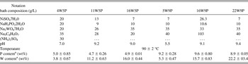
Phase transformation characteristics of the NiWP UBM were studied over Cu substrate (1 mm thick), while solder joint interface microstructure and drop impact resistance were investigated using a PCB as the substrate. Before the electroless plating, the surface of the Cu substrate was cleaned with acid and activated with Pd. Tungsten alloying was made by adding various amounts of W salts to the electroless nickel bath, and the composition of six baths are presented in Table I. NiWP films with three W levels and two P contents are denoted by their W and P contents (in wt.%), such as 4W5P, etc. The electroless NiWP films were typically 5 to ~7 um thick and subsequently immersion Au plated (0.1 um thick) except for the DSC and XRD specimens. DSC was conducted under the heating rate of 10 °C/min in N2 and XRD was used to characterize phase transformation characteristics of bare NiWP films. Solder joints were made by reflowing Sn–3.5Ag solder balls (with the diameter of 760 um) on the NiWP UBM at 260 °C for 1 min and the joint microstructure was analyzed using SEM equipped with energy dispersive x-ray spectroscopy (EDX). Impact resistance of the solder joints were measured by conducting drop tests according to the Joint Electronic Devices Engineering Council (JEDEC) JESD22-B111 under the peak acceleration of 1500 G, and the threshold resistance of 10 Ohms was used as the criterion of failure. The tests were interrupted when failure did not occur up to 300 drops.
Compositions of the six electroless NiWP baths and plating conditions.

a In the electroless film.
III. RESULTS AND DISCUSSION
A. DSC results
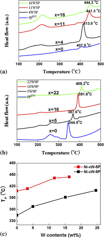
The DSC curves of NiWP films with varying P and W contents are given in Fig. 1. The DSC curve typically shows two exothermic peaks; a broad one at low temperature and a sharp one at high temperature. The broad peaks are related to the recovery of crystal defects and grain growth during the isochronic heating,Reference Hentschel, Isheim, Kirchheim, Muller and Kreye18 while the sharp peaks can be ascribed to the precipitation of Ni3P from the nanocrystalline Ni–xW–5P phases, or to the decomposition of the amorphous Ni–xW–9P phase into crystalline Ni and Ni3P. The main feature of DSC curves is better illustrated in Fig. 1(c), which shows the center position of the second exothermic peaks. Note that the peak temperature increased with the W content in the film, and that the phase transformation occurred at lower temperature in Ni–xW–9P films than in Ni–xW–5P films. Being metastable, Ni–xW–9P films precipitated Ni3P more readily, and the presence of W stabilized both Ni–xW–5P and Ni–xW–9P films by suppressing Ni3P precipitation.Reference Antonelli, Allen, Johnson and Dubin19
Variation of heat flow (measured by DSC) under isochronic heating with the W content in the (a) Ni–xW–5P and (b) Ni–xW–9P films.Reference Song and Yu21 (c) Shift of the peak temperature (T p) with the W content in Ni–xW–5P and Ni–xW–9P films.

B. XRD analyses
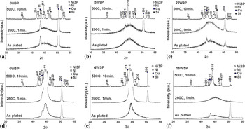
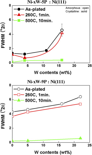
As-prepared and heat-treated NiWP films were analyzed by XRD and the results are presented in Fig. 2. It can be seen that all as-plated Ni–xW–5P and Ni–xW–9P films remained stable after the heat treatment of 1 min at 260 °C, which is a typical reflow condition of soldering. Thus, a typical reflow treatment did not affect the crystal structure of NiWP films significantly. However, all films decomposed into Ni and Ni3P after heat treating 10 min at 500 °C. Qualitative information on the crystallinity of electroless NiWP films can be found by measuring the full width at half-maximum (FWHM) of the Ni(111) peak, and the result is shown in Fig. 3. In the case of Ni–xW–5P films, crystallinity of as-plated and heat-treated films (260 °C, 1 min.) deteriorated abruptly above 11 wt.% W. Thus, Ni–5P films, which are typically nanocrystalline in the as-plated condition, can remain in the amorphous state even after reflow of 1 min at 260 °C when enough W (16 wt.% in this case) is added to the films. Note from the FWHM data that the reflow treatment had only marginal effects on the crystallinity of 16W5P and Ni–xW–9P films. In the case of Ni–xW–9P films, which were amorphous in the absence of W, addition of W up to 22 wt.% further increased FWHM. However, after the heat treatment of 10 min. at 500 °C, FWHM dropped markedly as amorphous films transformed to Ni and Ni3P. Even though a reflow treatment did not affect FWHM significantly, the intensity of the Ni(111) peak of 0W5P and 4W5P films did increase, as shown in Figs. 2(d) and 2(e), presumably due to the recovery and grain growth of the nanocrystalline films during the reflow process as mentioned in Sec. III. A.
XRD patterns out of the (a) 0W9P, (b) 5W9P, (c) 22W9P, (d) 0W5P, (e) 4W5P, and (f) 16W5P films after heat treatments; as plated, reflowed (1R, 260 °C × 1 min) and 500 °C × 10 min.

Measured FWHM of Ni (111) peaks after several heat treatments.

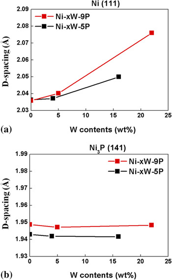
Effects of W concentration in the NiWP UBM on the interplanar spacing of Ni and Ni3P crystals, which precipitated during the heat treatment at 500 °C (10 min) are presented in Fig. 4. In contrast to the Ni lattice that dilated with the W content in the film, the Ni3P lattice parameter did not seem to be affected by W content in the UBM. Dilation of the Ni lattice with the W content in the film was more apparent in Ni–xW–9P films. This suggests that W atoms partition in the Ni lattice because W is quite soluble in the Ni solid solution, but W solubility in Ni3P is very limited or the (Ni,W)3P stoichiometry is quite stable. Dilation of the Ni lattice by the W partitioning is consistent with the Vegard’s Law.Reference Yang, Lim, Kumar, Lee and Chen20 Note that Ni lattice dilation for a given W addition was larger in Ni–xW–9P UBM than in Ni–xW–5P UBM, presumably because the amount of W that can partition into the Ni lattice became relatively larger for the former as more Ni atoms were tied up as Ni3P. The reason why the lattice parameter of Ni3P out of the Ni–xW–9P film is larger than that out of the Ni–xW–5P film is not understood at the moment.
Variation of interplanar spacing of (a) Ni(111) and (b) Ni3P(141) planes measured by XRD with the W content of the NiWP films.

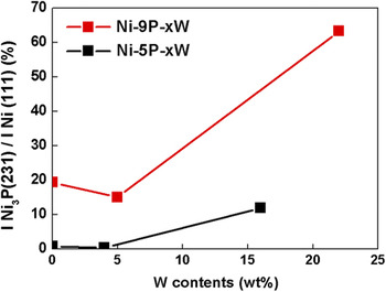
Figure 5 shows the intensity ratio between Ni3P(231) and Ni(111) XRD peaks of the NiWP films after the heat treatment at 500 °C. It can be seen that the amount of Ni3P precipitation increased with the W and P content of the film. The decomposition of NiWP film into Ni3P and Ni(W) is written as

X-ray peak height ratios between Ni3P(231) and Ni(111) peaks in the NiWP films after heat treatment at 500 °C × 10 min.

if there is no W partitioning in the Ni3P phase. Here, a, b, and c are the atomic fractions of Ni, W, and P in the as-plated UBM, i.e., a + b + c = 1. However, that cannot explain the large variations of Ni3P intensities as shown in Fig. 5. Here, we assume that W partitions in the Ni3P phase as in the Ni lattice and rewrite Eq. (1) as

Tungsten partitioning parameters y and z are related by

Thus, if the P content in the UBM is fixed (constant c) and the W content in the Ni lattice increased linearly with the W content in the film as shown in Fig. 4(a), i.e., y = αb where α is a proportionality constant, Eq. (3) states that the partitioning of W in the Ni3P increases with the W content in the film, i.e., z ~ b. The accelerated precipitation of Ni3P with the W content in the film can be understood in the same context. Because W partitions in Ni3P, XRD peaks coming from (Ni,W)3P increase due to the large atomic scattering factor of W, as shown in Fig. 5. Molar ratio between the Ni3P and Ni(W) phases is given by c/(a + b-3c) = c/(1–4c), and the amount of Ni3P precipitation during the heat treatment increased with the P content in the film.
C. Interfacial reactions
1. Ni–xW– 5P UBM
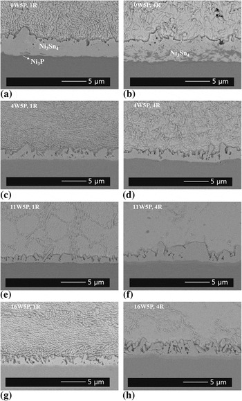
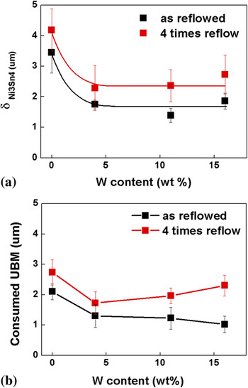
Backscattered SEM images of Ni–xW–5P/Sn–3.5Ag solder joints, reflowed one (1R) or four times (4R) at 260 °C for 1 min, are presented in Fig. 6. It can be seen that Ni3Sn4 did not spall off in all the specimens. The thickness of Ni3Sn4 after one (1R) and four (4R) reflows were measured and plotted as a function of W content of the UBM in Fig. 7. An addition of 4 wt.% W reduced Ni3Sn4 growth by half, but further addition of W did not show noticeable effects. Because Ni3Sn4 formed by the diffusion of Ni atoms from the Ni(P) UBM to the solder,Reference He, Chen and Qi6 W in the UBM is thought to work as a diffusion barrier of Ni atoms.Reference Cullity and Stock17, Reference Antonelli, Allen, Johnson and Dubin19 There were small amounts of voids and vertical cracks in the Ni3P layer, as shown in Figs. 6 and 8. The latter could be ascribed to the evolution of tensile stress accompanying the phase transformation of Ni(P) UBM, while the voids between the Ni3Sn4 IMC and UBM could form as a result of the Kirkendall effect.
Solder joint microstructure of Sn–3.5Ag/Ni–xW–5P after one and four reflows.

(a). Ni3Sn4 thickness as a function of the W contents in the Sn–3.5Ag/Ni–xW–5P joints after one and four times reflows. (b) Thickness of consumed UBM.

2. Ni–xW–9P UBM
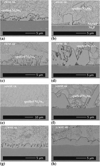
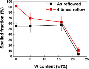
Selected SEM micrographs of Sn–3.5Ag/Ni–xW–9P solder joints reflowed one (1R) or four (4R) times are presented in Fig. 8. In the Ni–9P film without W (0W9P), Ni3Sn4 spalled off severely from the Ni–9P UBM after a single reflow as reported in the literatures.Reference Song and Yu3–Reference Jee, Yu and Ko7 Additions of 5 and 16 wt.% W to the UBM were effective but did not suppress the IMC spalling completely. However, an addition of 22 wt.% W to the UBM prevented IMC spalling completely even after four reflows. It can be seen that the Ni3P layer was not clear in NiWP UBM, but very clear in Ni5P and Ni9P UBM, as shown in Figs. 6 and 8. That could explain the TEM result presented in Fig. 12. It was shown that W in Ni(P) UBM suppressed the crystallization of Ni3P phase compared to crystalline Ni3P in Ni(P) UBM, amorphous (Ni,W)3P was rather difficult to observe from the SEM micrographs. Variation of the spalling characteristics of Ni3Sn4 with W content in the UBM are quantitatively presented in Fig. 9 by measuring the line fractions of the Ni3Sn4/UBM interface, which showed IMC spalling over the SEM micrographs. The result indicates that more than 20 wt% W should be added to the Ni–9P UBM to suppress the IMC spalling effectively.
Solder joint microstructure of Sn–3.5Ag/Ni–9P–xW after one and four reflows.

The interface line fraction of spalled IMC for Sn–3.5Ag/Ni–xW–9P joints after reflows.

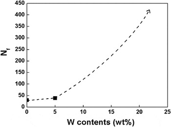
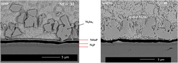
Effects of W on the drop impact reliability can be focused in the most straight forward manner from the drop test data shown in Fig. 10. Here, the number of drops-to-failure (N f) of Sn–3.5Ag/Ni–xW–P joints reflowed one time is plotted as a function of the W content of the UBM. It can be seen that 0W9P and 5W9P specimens showed low resistance to the drop impact fracture (N f < 50), however the drop impact resistance increased remarkably (N f > 300) in the case of the 22W9P specimen, which can be ascribed to the suppression of the IMC spalling. Failure loci of Ni–xW–9P specimens after the drop tests are shown in Fig. 11. In the case of Ni–9P specimens without W, brittle fracture occurred through the NiSnP layer, which is known to form between Ni3P and Ni3Sn4 and cause Ni3Sn4 spalling,Reference Sohn and Yu5 and the same was true of the 5W9P specimens. In the case of 22W9P specimens, formation of Ni3P and NiSnP were apparently suppressed by the presence of 22 wt.% W in the UBM and brittle failure did not occur up to 300 drops.
Number of drops to failure (N f) of as-reflowed Ni–xW–9P specimens.

Micrographs showing failure loci of as-reflowed Ni–xW–9P specimens.

Previous XRD analysis showed that the 22W9P film remained amorphous after the 1R reflow. The interface microstructure of Sn3.5Ag/Ni22W9P joints after one reflow was analyzed using TEM and the presence of an amorphous (Ni,W)3P layer between the amorphous UBM and Ni3Sn4 was found. Figure 12 shows SEM and TEM micrographs from the joint interface along with diffraction patterns from the two layers adjacent to Ni3Sn4. A dark layer (marked B), which was 0.5 ~ 1.0 μm thick, was identified between unreacted UBM (denoted as A) and Ni3Sn4, and subsequent diffraction analysis showed a typical ring pattern of the amorphous structure. As the chemical composition of the layer was identified [by EDX] to be Ni:W:P = 61:12:27 in at.%, the layer was assumed to be (Ni,W)3P, which did not crystallize. Characteristics of the amorphous (Ni,W)3P layer is not well understood at the moment.
SEM and cross-sectional TEM micrographs [using focused ion beam (FIB) technique] and diffraction patterns from regions A and B.

IV. CONCLUSION
Additions of W to the electroless Ni–5P and Ni–9P films stabilized the thermal stability of the films and retarded their decomposition to higher temperature. The effect was most striking when 22 wt.% W was added to Ni–9P film, which remained amorphous even after several reflows. Tungsten addition not only dilated the Ni lattice by partitioning, but also enhanced Ni3P precipitation. The beneficial effect of the W addition was most clearly demonstrated in the drop tests, and the correlation between the drop impact resistance and the degree of spalling was evident. An addition of 22 wt.% W almost eliminated IMC spalling and the solder joints would not be broken even after 300 drops. TEM analysis illustrated the presence of an amorphous (Ni,W)3P layer between the Ni3Sn4 and the UBM. The effect of W on IMC thickness was rather marginal and most effective at 4 wt.%.
ACKNOWLEDGMENT
This work was supported by a National Research Foundation of Korea (NRF) grant funded by the South Korean Government (MEST) (Grant No. 2010-0000862).