


I. INTRODUCTION
High quality materials synthesis is one of the foremost prerequisites in condensed matter physics to gain deep insights into the electronic- and spin correlations of materials. Molecular beam epitaxy (MBE) is a vacuum deposition method in which well-defined thermal beams of atoms react at a crystalline surface to produce an epitaxial film. MBE was originally developed for the synthesis of GaAs Reference Cho and Arthur1 but due to its unprecedented ability to control layering at the monolayer level and compatibility with surface-science techniques to monitor the growth process as it occurs, its use has expanded to other material systems. A clean ultra-high vacuum deposition environment combined with in situ characterization during epitaxial growth, without highly energetic species are characteristics that distinguish MBE from other thin film synthesis methods used to prepare epitaxial oxides. These combined aptitudes are vital to the precise manipulation and customization of oxide heterostructures at the monatomic layer level. In addition to molecular beams emanating from electron-gun sources containing individual elements, molecular beams of gases may also be introduced; for example, to form oxides or nitrides. This variant of MBE is known as “reactive MBE”, in analogy to “reactive evaporation”, which takes place at higher pressures where well-defined molecular beams are absent.
The use of reactive MBE to grow multicomponent oxides started in 1985 for the synthesis of LiNbO3 by Betts and Pitt. Reference Betts2 Vivified by the discovery of high-temperature superconductivity, Reference Bednorz and Müller3 oxide MBE has since been used to grow the oxide superconductors (Y, La, Nd, Sm, Eu, Gd, Dy)Ba2Cu3O7−δ, Reference Oh, Naito, Arnason, Rosenthal, Barton, Beasley, Geballe, Hammond and Kapitulnik4–Reference Terashima, Iijima, Yamamoto, Bando and Mazaki12 La2−x Sr x CuO4, Pr2−x Ce x CuO4+δ, Nd2−x Ce x CuO4+δ, Reference Locquet, Gerber, Cretton, Jaccard, Williams and Machler13–Reference Krockenberger, Yamamoto, Mitsuhashi and Naito21 Ba1−x K x BiO3, Reference Enomoto, Murakami and Moriwaki22–Reference Utz, Wiest, Prusseit, Berberich and Kinder27 and Bi2Sr2Ca n−1Cu n O2n+4 Reference Schlom, Marshall, Sizemore, Chen, Eckstein, Bozovic, von Dessonneck, Harris and Bravman28–Reference Tsukada and Uchinokura34 for n = 1 − 11. It has also been used to grow ferroelectrics, Reference Sitar, Gitmans, Liu, Gunter, Speck, Fork, Wolf and Shiosaki35–Reference Eckstein, Bozovic, O'Donnell, Onellion and Rzchowski46 ferromagnets, Reference Roesler, Filipkowski, Broussard, Idzerda, Osofsky, Soulen and Bozovic47–Reference Chambers51 and multiferroic oxide materials Reference Kabelac, Ghosh, Dobal and Katiyar52–Reference Chye, Liu, Li, Lee, Lederman and Myers56 LuFeO3, Reference Moyer, Misra, Mundy, Brooks, Heron, Muller, Schlom and Schiffer57 and superlattices of these materials. Reference Bozovic, Eckstein, Virshup, Chaiken, Wall, Howell and Fluss58–Reference Moyer, Misra, Mundy, Brooks, Heron, Muller, Schlom and Schiffer57 The setup of a MBE system for the growth of multicomponent oxides differs in many ways from today's conventional MBE systems designed for the growth of semiconductors. The major differences are the required presence of an oxidation agent, a stern composition control, and scale up in pumping to manage the oxidant gas load. To oxidize the element species reaching the substrate to form the desired multicomponent oxide, a molecular beam of oxidant is used. To maintain the long mean free path necessary for the MBE process, pressures lower than 10−5 Torr are mandatory. Composition control is another significant challenge for oxide MBE Reference Yamamoto, Krockenberger and Naito71 ; improvements in composition control have led to significant progress in customizing oxide structures, perfecting superlattices, and achieving improved properties. The use of electron impact emission spectroscopy (EIES) Reference Lu, Blissett and Diehl72–Reference Lu, Lightner and Gogol74 or atomic absorption spectroscopy (AAS) Reference Du, Droubay, Liyu, Li and Chambers75 for oxide MBE composition control has allowed fluxes to be measured with an accuracy of better than 1 %. In situ reflection high energy electron diffraction (RHEED) oscillations during the shuttered MBE growth of multicomponent oxides has also been shown to provide a means to accurately calibrate fluxes. Reference Haeni, Theis and Schlom76 Oxide MBE has yielded films with the highest structural quality and most precise layering control at the atomic-layer level, e.g., infinite-layer Sr1−x La x CuO2, Reference Krockenberger, Sakuma and Yamamoto77 Sr11Ti10O31, Reference Lee, Podraza, Zhu, Berger, Shen, Sestak, Collins, Kourkoutis, Mundy, Wang, Mao, Xi, Brillson, Neaton, Muller and Schlom78 and Bi2Sr2Ca0.5(Ca,Dy)10Cu11O26. Reference Klausmeier-Brown, Virshup, Bozovic, Eckstein and Ralls30 It is the combination of above mentioned advantages that make oxide MBE the method of choice when it comes to achieving the intrinsic properties of materials. Reference Schlom79 For example, Pr2CuO4+δ is a superconductor on the verge of becoming an antiferromagnetic insulator. To date, the only technique that has succeeded in achieving this superconducting ground state in as-grown films is oxide MBE. Reference Krockenberger, Horio, Irie, Fujimori and Yamamoto17
II. RESULTS AND DISCUSSION
Oxide MBE has yielded films with the highest structural quality and most precise layering control at the atomic-layer and we therefore adopted this approach for the synthesis of Pr2−x
Ce
x
CuO4+δ thin films. In particular it is the electron-doped cuprates system that caught our attention more than two decades ago
Reference Naito and Sato14
while knowing that the true challenge of this superconductor goes well beyond a perfect cation arrangement. In light of recent advancements on the comprehension of the growth of complex oxide materials
Reference Lee, Luo, Tung, Chang, Luo, Malshe, Gadre, Bhattacharya, Nakhmanson, Eastman, Hong, Jellinek, Morgan, Fong and Freeland80
the synthesis of high-quality Pr2−x
Ce
x
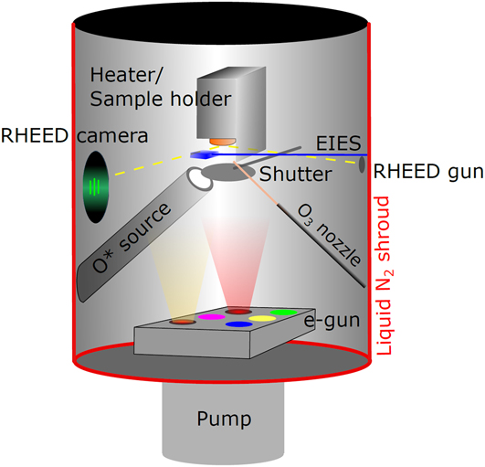
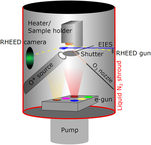
CuO4+δ thin films still remains a major challenge. In Fig. 1 we show a scheme of our oxide MBE setup used for the growth of Pr2−x
Ce
x
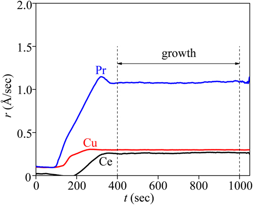
CuO4+δ thin films. EIES was used to monitor and control Pr and Cu fluxes and due to weak relative electron impact emission intensities of Ce dopants
Reference Marin, Cornejo and Arriagada81
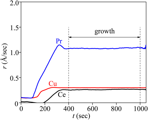
we used a shielded quartz-crystal rate-control system for high precision rate control exclusively for Ce. The absolute deposition rate of each constituent element is shown in Fig. 2. Without limitations of generality we used ozone generated from a silent discharge ozone generator as an oxidizing agent (see Fig. 1). A constant substrate temperature of 700 °C was maintained using a custom designed resistive heater stage which is monitored by a pyrometer. The atomic structure of the Pr2−x
Ce
x
CuO4+δ thin films and Pr2−x
Ce
x
CuO4+δ–SrTiO3 interface was investigated by means of high resolution (scanning) transmission electron microscopy (HRSTEM). A JEOL JEM-ARM 200F (JEOL Ltd., Tokyo, Japan) STEM with a spherical aberration correction, operated at 200 kV.
Reference von Harrach, Dona, Freitag, Soltau, Niculae and Rohde82
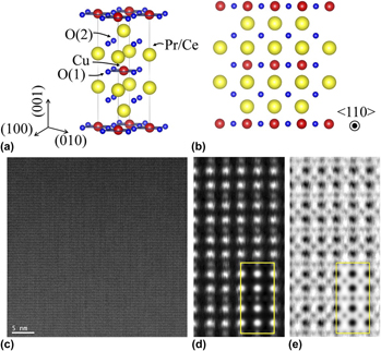
For atomic-scale chemical mapping, energy dispersive x-ray spectroscopy (EDS) spectral image data was acquired with an electron probe of size ∼1.0 Å, convergence angle of 18–22 mrad, and current of ∼23–68 pA. High-angle annular dark-field (HAADF) images were recorded under similar optical conditions using an annular detector with a collection range of 90–370 mrad. Spectral images were acquired as a series of frames, where the same region was scanned multiple times. Frames were spatially drift-corrected to build up spectral image data. The instantaneous dwell time on each pixel was 38.5 µs, and a typical frame was 512 × 512 pixels. Spectral image collection typically took about 10 s, yielding a total per-pixel dwell time of about 38 ms. The epitaxial character of the deposited films are evident from Fig. 3, which shows a HAADF image of the interface region of a representative Pr2−x
Ce
x
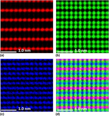
CuO4+δ sample in (110) viewing direction. Using HAADF conditions the atomic columns cause bright contrast, whereas the intensity of the maxima increases with atomic number from CuO columns via PrO, producing an additional chemical contrast. Apparently, Ce is homogeneously distributed at Pr positions as a possible superstructure remains elusive [see Fig. 3(c)]. Figure 4 shows atomic resolution HRSTEM EDS mappings of the Pr2−x
Ce
x
CuO4+δ thin films synthesized by reactive MBE. EDS mapping was performed using a JEOL JEM-ARM 200F HRSTEM (JEOL Ltd.) equipped with a Wien filter.
Reference Rose83
Pr and Cu maps clearly reveal the formation of the characteristic chemically ordered T′ structure. For thin TEM specimens, the EDS signal is localized to atomic columns.
Reference Lu, Xiong, Benthem and Jia84,Reference Allen, Findlay, Lupini, Oxley and Pennycook85
Furthermore, under such conditions, EDS x-ray counts from individual atomic columns can be approximated by a Gaussian distribution and thus be properly integrated by fitting Gaussian peaks at each atomic column position
Reference Lu, Romero, Lee, MacManus-Driscoll and Jia86
; the chemical composition at the atomic column positions can then be calculated column-by-column using the Cliff–Lorimer method.
Reference Cliff and Lorimer87
The width of the Gaussian peak, defined as the full-width at half-maximum (FWHM), which ultimately determines the spatial resolution of the chemical mapping, is effectively determined by convoluting the electron probe with the effective EDS local ionization potential under thin specimen conditions. By selecting a small electron probe (∼1.0 Å) and an appropriately thin area on the specimen, the spatial resolution of chemical mapping can be improved. The specimen thickness for the approximation to be valid must be limited to be less than 30 nm. The selection of small electron probe and thin specimen leads, however, to significant reduction in x-ray count. This reduction can be compensated by lattice-averaging EDS maps that are related by lattice translation vectors, effectively improving the EDS counting statistics. It is intriguing to see to what extent, if any, the superconducting state is influenced by the appearance of crystallographic defects. It is worth to state that although the mean free path lengths
 $\ell$
vary a lot, there is little to no influence on the superconducting transition temperature seen. This becomes only prominent for very short
 $\ell$
, or when residual resistivity ratio RRR = ρ(300 K)/ρ(1.8 K) < 2. In that case, however, one would approach the Ioffe–Regel limit which coincides with the onset of long-range antiferromagnetic order as concentration of occupied apical sites increases.
Reference Kojima, Krockenberger, Yamauchi, Miyazaki, Hiraishi, Koda, Kadono, Kumai, Yamamoto, Ikeda and Naito88
In Fig. 5, we show the temperature dependence of the magnetization taken zero-field-cooled (ZFC) and field-cooled-cooling (FCC) modes. The diamagnetic signal at 1.8 K for the films with RRR ≥ 8 is −8.4 memu in ZFC mode, whereas it is significantly weaker for Pr2−x
Ce
x
CuO4+δ thin films with RRR ≈ 4. The continuous variation of the diamagnetic signal originating from the superconducting states of Pr2−x
Ce
x
CuO4+δ may allow for two interpretations. One is that the amount of the superconducting condensate depends on the amount of available carriers that could form the superconducting instability at the Fermi surface. As Pr2−x
Ce
x
CuO4+δ with small RRR values are less conducting than films with large RRR values, a reduced superconducting volume appears as a reasonable explanation. Another assumption is that Pr2−x
Ce
x
CuO4+δ films with small RRR have a higher concentration of defects or impurity states, thus the scattering probability is enhanced.
Reference Finkelman, Sachs, Droulers, Butch, Paglione, Bach, Greene and Dagan89
These defects may persist into the superconducting state and form localized nonsuperconducting clusters that allow for penetration of the magnetic field. We now turn to the question on how the observed changes in
 $\ell$
are reflected in the Hall coefficient R
H which is shown in Fig. 6. For small
 $\ell \approx 12.6\;{\rm{nm}}$
, the Hall coefficient is negative over the entire temperature range measured. This is not surprising as for decades it is believed that such behavior is intrinsic to electron doped cuprate superconductors. It is also known that the Fermi surface of so-called electron doped cuprates is hole-like, not electron like, as shown by angle-resolved photoemission spectroscopy (ARPES) experiments.
Reference King, Shen, Dessau, Wells, Spicer, Arko, Marshall, DiCarlo, Loeser, Park, Ratner, Peng, Li and Greene90
Also shown in Fig. 6 is the Hall coefficient for a Pr2−x
Ce
x
CuO4+δ thin film with
 $\ell \approx 75.8\;{\rm{nm}}$
. Its temperature dependency is quite different from the previous one. In contrast to the Pr2−x
Ce
x
CuO4+δ with
 $\ell \approx 12.6\;{\rm{nm}}$
, this Hall coefficient is positive at low temperatures.
Reference Brinkmann, Rex, Stief, Bach and Westerholt91
Generally, the Hall coefficient is proportional to
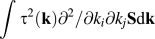 $\mathop {\int {{\tau ^2}\left( {\bf{k}} \right){\partial ^2}/\partial {k_i}\partial {k_j}{\bf{S}}{\rm{d}}{\bf{k}}} }\nolimits^$
and one requires detailed knowledge of the topology of the underlying Fermi surface S. Changing the sign of the Hall coefficient points to significant modifications at the Fermi surface either by shape or by matrix elements of the scattering time
 $\tau \left( {\bf{k}} \right)$
. Comparing the superconducting transition temperatures (inset of Fig. 6) for Pr2−x
Ce
x
CuO4+δ with
 $\ell \approx 12.6\;{\rm{nm}}$
and 75.8 nm emphasizes that there is no change at all. Instead, the only noticeable change stems from the enhancement of
 $\ell$
and that in turn promotes a scenario where the scattering time of hole-like charge carriers is enhanced and that this enhancement is driven by annealing. In particular, the annealing process is known to trigger the evacuation of occupied apical sites in electron-doped cuprates
Reference Krockenberger, Yamamoto, Tsukada, Mitsuhashi and Naito19,Reference Radaelli, Jorgensen, Schultz, Peng and Greene92–Reference Schultz, Jorgensen, Peng and Greene95
and these occupied apical sites have been found to enhance the antiferromagnetic correlation length.
Reference Krockenberger, Eleazer, Irie and Yamamoto96
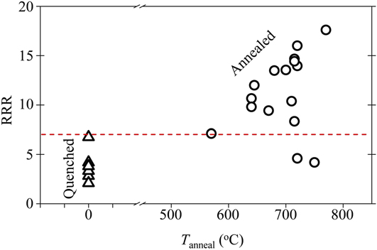
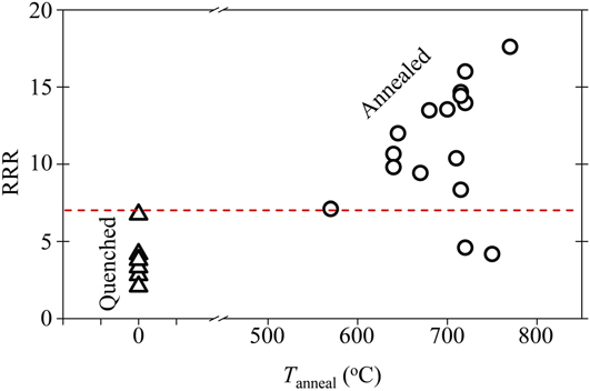
The influence of the antiferromagnetic correlation length on the mean-free path length can be seen in Fig. 7 where the residual resistivity ratio of Pr2−x
Ce
x
CuO4+δ thin films is plotted as a function of the annealing temperature. This RRR value can be enhanced by progressively increasing the annealing temperature while keeping in mind that one must obey the thermodynamic limit set by the decomposition of Pr2−x
Ce
x
CuO4+δ. On the other hand, however, if the annealing process time exceeds certain limitations, oxygen defects will emerge within the CuO2 planes and superconducting transition temperature T
c inevitably decreases. For optimally annealed Pr2−x
Ce
x
CuO4+δ, as T
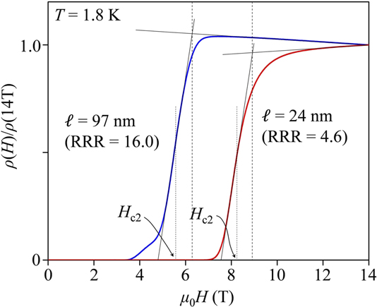
c remains constant and one is left therefore with the criteria of the mean-free path length to determine defect concentrations. Scattering processes initiated by such defects not only influence the normal state electron correlations but also the superconducting state. In Fig. 8 we plot the normalized magnetoresistance of Pr2−x
Ce
x
CuO4+δ thin films with
 $\ell = 97$
and 24 nm. For
 $\ell = 97\;{\rm{nm}}$
, the upper critical field H
c2 value is certainly smaller than that observed for Pr2−x
Ce
x
CuO4+δ with
 $\ell = 24\;{\rm{nm}}$
and this result points toward an intrinsically clean superconductor having a longer coherence length ξGL when compared to superconducting Pr2−x
Ce
x
CuO4+δ with
 $\ell = 24\;{\rm{nm}}$
. This result appears to be in contrast to reports showing that electron-doped cuprate superconductors are intrinsically in the dirty limit.
Reference Dagan, Beck and Greene97
Reactive molecular beam epitaxy setup for the synthesis of complex transition metal oxides. Constituent elements are evaporated by electron guns and the flux of each element is monitored and controlled by EIES. The system is equipped with a RF oxygen source as well as an ozone injector.
Evaporation rate profiles of Pr, Cu, and Ce prior and during the synthesis of Pr2−x Ce x CuO4+δ.
Crystal structure (a, b) and HAADF-STEM images (c, d, e) of Pr2−x Ce x CuO4+δ thin films grown by reactive molecular beam epitaxy onto SrTiO3 substrates. Simulated images are inset in (d, e). The superconducting transition T c ≈ 20.0 K.

(a) EDS map of Cu Kα; (b) EDS map of Pr/Ce Lα; (c) EDS map of O Kα; (d) composite color map of Cu Kα (red), O Kα (blue), and Pr/Ce Lα (green). The superconducting transition T c ≈ 20.0 K.

Diamagnetic shielding of Pr2−x
Ce
x
CuO4+δ thin films recorded for various values of
 $\ell$
. In (a), (b), (c), and (d),
 $\ell$
is 108.0, 75.8, 24.2, and 21.3 nm, respectively. Note that the external magnetic field (10 Oe) was applied perpendicular to the film surface and perpendicular to the CuO2 planes of the Pr2−x
Ce
x
CuO4+δ thin films.

Temperature dependency of R
H of Pr2−x
Ce
x
CuO4+δ thin films recorded for
 $\ell$
= 12.6 and 75.8 nm, respectively. The inset shows the corresponding resistivity behaviors of samples A and B.

Residual resistivity ratio plotted as a function of the annealing temperature used on Pr2−x Ce x CuO4+δ thin films after the growth. For annealing temperature equal “0”, we skipped the annealing procedure.
Normalized magnetoresistance of Pr2−x
Ce
x
CuO4+δ thin films as a function of the magnetic field applied perpendicular to the CuO2 planes for
 $\ell$
= 97 nm, and 24 nm, respectively.
III. CONCLUSION
In summary we have shown that electron-doped cuprate superconductors with the T′ structure can be varied in a way that allows for large changes in
 $\ell$
. We used a custom designed reactive MBE setup equipped with electron guns which are controlled by EIES for the synthesis of ultra-clean Pr2−x
Ce
x
CuO4+δ thin films. We analyzed defects at the atomic level by HAADF-STEM and found that while the cation arrangements in films grown by reactive MBE are nearly perfect we remain cautious on anionic defects as it is challenging to precisely pinpoint their locations in the crystal. Our results show that the electron correlations observed in cuprate superconductors are indeed closely related to anionic defects brought by the synthesis method. Limiting this anionic defect-concentration is one of the foremost challenges in condensed matter physics and vital to the comprehension of the electronic correlations that partake in cuprate superconductors. In contrast to earlier reports where electron-doped cuprate superconductors are reported to be in the dirty limit, our novel synthesis methods allow us to gain insights on how defects tune the underlying electron correlations in Pr2−x
Ce
x
CuO4+δ.
ACKNOWLEDGMENTS
The authors thank Takayuki Ikeda for his contribution in STEM and EDS measurements. Discussions with Robert Hammond, Michio Naito, and Ivan Bozovic have been highly appreciated.