

I. INTRODUCTION
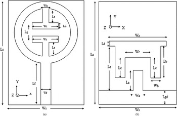
Commercially used Ultra Wideband (UWB) systems need small low cost antennas, which have omni directional radiation pattern, wideband characteristics and significant gain. These features can be obtained with the help of planar monopole antennas. Thus planar monopoles are widely used in UWB applications [1] and advance research activities. Since UWB systems cause electromagnetic hindrance to various narrowband wireless communication systems operating between the frequencies range of 3.1 and 10.6 GHz, we need to design UWB antennas with tunable notched bands [Reference Ren and Kai2]. In order to produce notched band, various modified planar monopoles are being used [Reference Yazdanifard, Sadeghzadeh and Ojaroudi3–Reference Tilanthe, Sharma and Bandopadhyay16]. Slots of various shapes such as trapezoid [Reference Yazdanifard, Sadeghzadeh and Ojaroudi3] and wedge shaped [Reference Ojaroudi4] are used to generate tunable notched band. The geometry of the proposed antenna is shown in Fig. 1. Figure 1(a) shows the top view of the proposed antenna and Fig. 1(b) shows its bottom view.
Geometry of the proposed antenna. (a) Top view of the proposed antenna. (b) Bottom view of proposed antenna.

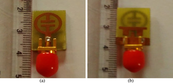
The gain of the proposed antenna is improved with the use of a π-shaped strip and a rectangular strip in the ground plane. The notched band is tuned by varying the air gap “L g ” between two T-shaped strips, which are coupled electromagnetically. Figure 2 shows the fabricated prototype antenna.
Fabricated antenna prototype. (a) Top view of the fabricated antenna. (b) Bottom view of fabricated antenna.

II. ANTENNA DESIGN
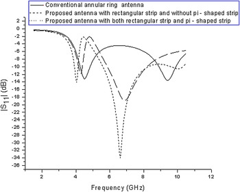
The proposed microstrip fed antenna is printed on FR4 substrate of height 1.6 mm; permittivity ε r = 4.4, and loss tangent 0.02. Ansoft High Frequency Structure Simulator (HFSS) is used for the simulation process of the designed antenna. The proposed antenna has been designed in three steps. In the first step, the basic antenna design includes a conventional annular ring radiating patch with a conventional ground plane of length “L gd ” = 4 mm and width “W s ” = 12 mm. This antenna design offers bandwidth from 4.3–5 to 8.9–9.9 GHz at −10 dB. The second step has modified antenna design, resulting band notching by including a pair of T-shaped strips in the radiating patch and improved bandwidth by modifying the ground plane by adding a rectangular strip. In the third step; in order to achieve larger bandwidth the ground plane of the antenna is modified by including an additional π-shaped strip above the conventional ground plane.
The structure of the antenna consists of an annular patch, a microstrip feed line, and a ground plane. The annular patch consists of one outer circle of radius 5 mm and inner circle of radius 4 mm. The length and width of feed line are “L f ” and “W f ”, respectively. The bottom portion of antenna consists of ground plane (conducting) of length “L gd ” and width “W s ”. The proposed antenna is also provided with SubMiniature version A (SMA) connector of 50-Ω for the transmission of signal. By varying the antenna parameters “L g ” and “W t ” carefully the tunable notched band can be achieved.
The optimized dimensions of the proposed antenna are as follows:
“W s ” = 12 mm, “L s ” = 18 mm, “W f ” = 2 mm, “L f ” = 7 mm, “W u ” = 1 mm, “L t ” = 2.5 mm, “W t ” = 5 mm, “L u ” = 1.2 mm, “L g ” = 1.4 mm, “L a ” = 3.5 mm, “W a ” = 1 mm, “L e ” = 3.75 mm, “W d ” = 10 mm, “L b ” = 3 mm, “W c ” = 4 mm, “L c ” = 2.5 mm, “W b ” = 1.5 mm, “L d ” = 0.5 mm, “L gd ” = 4 mm.
III. RESULTS AND DISCUSSION
This section contains simulated and measured results of the proposed antenna. Fabricated antenna has been characterized for its return loss characteristics by Rohde and Schwarz vector network analyzer (Model-ZVA40).
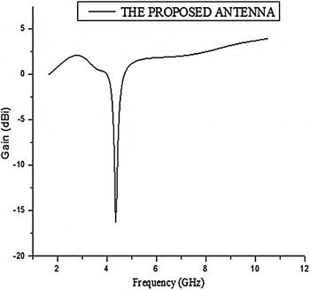
Figure 3 shows gain versus frequency curve of the proposed antenna. The antenna has a notched band in the frequency range of 4.2–6 GHz and has the lowest gain −16 dBi at 4.3 GHz. The gain is maximum at 10.45 GHz having value 4 dBi.
Gain versus frequency plot of proposed antenna.

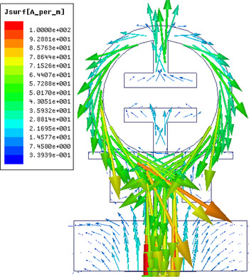
In order to explain the band notched characteristics of the proposed antenna with rectangular strip and π-shaped strip the simulated current distribution at 4.3 GHz is shown in Fig. 4. This current distribution shows that the band-notched characteristics are produced by the oppositely directed current along the T-shaped strips. On account of this oppositely-directed current distribution, the antenna impedance becomes high and the antenna does not radiate at this notching frequency.
Simulated current distribution for the proposed antenna with rectangular strip and π-shaped strip at 4.3 GHz.

Figure 5 shows reflection coefficient versus frequency curve of the proposed antenna. The conventional ordinary annular antenna without modified ground planes covers the −10 dB bandwidth from 4.3 to 9.9 GHz. By employing two T-shaped strips in the annular ring radiating patch and a rectangular strip in the ground plane the bandwidth of the proposed antenna lies in the frequency range of 4.2–8.3 GHz. Further, adding two T-shaped strips and a rectangular strip along with π-shaped strip the bandwidth of the antenna further increases and ranges from 3.5 to 10.6 GHz. This large bandwidth is obtained by elongated current path produced by rectangular strip added with conventional ground plane of the microstrip fed antenna and an additional Π-shaped strip placed above it. Hence, the modified ground shape of the antenna yields larger antenna bandwidth.
Simulated return loss characteristics for ordinary annular antenna, proposed antenna with rectangular strip and without π-shaped strip, proposed antenna with rectangular strip, and π-shaped strip.

A) Effect of antenna parameters on tunable notched band
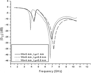
The variation in “W t ” and “L g ” highly influences the notched band frequencies. Figure 6 shows the variation of S 11 with different values of “W t ” and “L g ”. For “W t ” = 6 mm and “L g ” = 0.6 mm notched band ranges from 4.6 to 6.3 GHz. Similarly, for “W t ” = 5 mm and “L g ” = 1 mm notched band ranges from 4.6 to 6.1 GHz. For “W t ” = 4 mm and “L g ” = 0.6 mm notched band ranges from 4.2 to 5.8 GHz. Thus, by varying the values of the parameters “W t ” and “L g ”, tunability of the notched band can be achieved.
Return loss characteristics of the proposed antenna for different values of “W t ” and “L g ”.

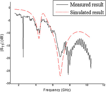
Figure 7 shows the measured and simulated return loss characteristics of the proposed antenna. The measured and simulated results are in good agreement with each other. The notched band is obtained from 4.2 to 6 GHz. The proposed design is smaller than design proposed in [Reference Moeikham, Mahatthanajatuphat and Akkaraekthalin5, Reference Zhang, Wang and Cheng6].
Simulated and measured return loss characteristics of proposed antenna.

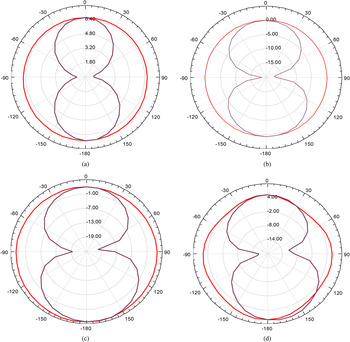
Figure 8 shows the radiation patterns of the proposed antenna. Radiation pattern obtained in H–plane (XZ–plane) is omnidirectional and in E-plane (YZ–plane) is bidirectional. Radiation patterns obtained at 4 and 5 GHz are purely omnidirectional, whereas the radiation patterns obtained at higher frequencies like 7.5 and 9.5 GHz are nearly omnidirectional due to excitation of higher modes at high frequencies.
Radiation patterns of proposed antenna at (a) 4 GHz, (b) 5 GHz, (c) 7.5 GHz, and (d) 9.5 GHz.

IV. CONCLUSION
We have reported in this paper miniaturized UWB antenna with tunable notched-band characteristics, which has been simple to design and fabricate. The bandwidth of the notched band can be tuned by changing the air-gap distance between two T-shaped strips placed inside the radiating annular patch. It has been found that the fabricated miniaturized UWB antenna covers the frequency range of 3.5–10.6 GHz for UWB systems with a notched band from 4.2 to 6 GHz. The designed antenna has omnidirectional radiation patterns with significant gain in the entire frequency band except the notched band.
ACKNOWLEDGEMENTS
The authors express warm acknowledgement to Dr. A. K. Sinha, Scientist, Dr. Hasina Khatun, Scientist, at CSIR-CEERI Pilani, India, Dr. A. K. Sharma, Global Institute of Technology, Jaipur and Dr. Deepak Bhatnagar of Rajasthan University for providing their research facilities for this work. Authors are also thankful to Er. Mayank Sharma of ECE department, Govt. Engineering College Ajmer, India for this work.
 Priyanka Sharma received her M.Tech. degree in Electronics and Communication from Arya College of Engineering and I.T. Kukas, Jaipur (Rajasthan) and is working there as lecturer.
 Kirti Vyas received her M. Tech. degree in Electronics and Communication from Malviya National Institute of technology, Jaipur, Rajasthan, India. She is Professor at Arya College of Engineering and I.T., Kukas, Jaipur (Rajasthan) and has about 20 international papers to her credit. Her main research interests are design and optimization of planar antennas and array.
 Dr. Rajendra Prasad Yadav completed his Ph.D. (Communication Engineering) from MREC Jaipur (University of Rajasthan) and M.Tech (Integrated EC & Circuits) from Indian Institute of Technology Delhi. Currently, he is working as Professor, in the department of Electronics Engineering, Malvia National Institute of Technology, Jaipur (Rajasthan), India. He was instrumental in formulating Ph.D. Ordinances and starting research work in RTU Kota as Vice Chancellor. He has 65 research publications to his credit. His research interest is Error Control Codes and MIMO-OFDM, RF and Antenna Systems, Mobile and Wireless Communication Systems, Optical Switching and Materials, Mobile Adhoc and Sensor Network, Device Characterization and MEMS.