I. INTRODUCTION
The most flexible satellite to ground/airplane communication systems are based on phased array antenna technology. Unfortunately, the cost of phased array antennas is related to the number of active elements, making the systems too expensive for many commercial/military applications. The mechanically scanning antennas resulted from phased arrays are also expensive, which force the use of electro-mechanical actuator. These are usually bulky and prone to mechanical failure.
Phase shifters are then emerged for electronic beam scanning and beam directing. Phase shifters were mostly designed with passive components in earlier stages. Some of the methods could bring correct time delay, but most of them were impractical for integration with multiple arrays in a commercial process because of their physical dimensions. Most of them need typically, more than two stages to compensate for their large loss. In comparison with passive phase shifters, planar phase shifters provide continuous phase shift with lower loss. This will result the increased usage of phase shifters to scan signals in frequency agile systems. There is also a significant demand in the wireless and microwave industries for affordable phase shifters that can reduce the cost of an electronically scanned antenna system and allow them to be deployed more widely. Thus, it is an important issue to investigate suitable phase-shifters according to the requirements of various system applications.
This paper presents a simple design of linear planar phase shifter deployed with defected ground structure (DGS). A microstrip–conductor-backed coplanar waveguide–microstrip (MP–CBCPW–MP) transition line is implemented to enhance the phase characteristics. The entire operation utilizes 700 MHz band which is used for commercial multimedia broadcasting, digital television, and local public safety network in regulated channels (available at: http://www.fcc.gov/pshs/public-safety-spectrum/700-MHz/).
Microstrip–slot line transitions has been implemented with air bridges for matching transition modes [Reference Ma, Yongxi and Itoh1]. The same technique is replaced with chip resistors and used in MP–coplanar strips (CPS)–MP transition [Reference Wu, Zhang, Dong and Zhang2]. The mode matching using integrated device yields 180° phase shift with Wilkinson arrangement of the transition. Phase shifters utilizing microstrip–slot transition technique has been reported to obtain ±90° phase [Reference Wang, Bialkowski and Abbosh3]. A virtual short and open-circuit termination has been used with acceptable insertion loss.
CPW–MP transition techniques using silicon membranes have been intensively used for wider range of frequencies [Reference Zheng, Papapolymerou and Tentzeris4]. The method resulted in addition of layers and substrate modifications to PCBs [Reference KulandhaiSamy, Arun Kumar and Kanagasabai5]. Meanwhile, grounded CPW transition gives miniaturized design utilizing micromachining techniques for W band operations [Reference Raskin, Gauthier, Katehi and Rebeiz6]. These complex manufacturing techniques in CPW–MP transitions has been revolutionized with CBCPWs. The CBCPW has been initially endorsed for its dispersion characteristics by Shih and Itoh [Reference Shih and Itoh7], by characterising the slot spacing with phase constants. For wide range of frequencies, micro electro–mechanical systems (MEMS) phase shifters has been used to get different phase states [Reference Rebeiz, Tan and Hayden8]. In radio frequency (RF) MEMS phase shifters, MEMS capacitive and discrete switches are used to achieve a phase shift with electrostatic actuation. A reconfigurable photonic band gap (PBG) ground plane is proposed [Reference Elamaran, Chio, Chen and Chiao9] where four-element patch array is used for beam steering. The control of wave phenomenon with PBG ground plane elements is achieved using switches and parasitic components. Beam steering of 6° to 35° is attained using the selection of PBG holes.The concept of PBG holes motivated higher phase tunable coupled line phase shifter using DGS [Reference Sang-Min, Chul-Soo, Seong-Soo, Dal and Itoh10]. Two DGS elements are switched using varactor diodes to get higher phase tuning property. Because of switching, constant phase over a band of 1–3 GHz is attained, resulting in switching delay.
Microstrip phase shifter using reconfigurable ground plane is also reported [Reference Shafai, Sharma, Shafai and Chrusch11]. Silicon wafer membrane is used to enable control of transmission line to ground plane spacing. Micromachining is used to fabricate thin-film copper membranes in the ground plane below the transmission line. Different membrane geometries are also investigated to achieve different phases. Both single and multiple series ground-plane membranes are possible, and they can be activated with discrete or continuous control signals, individually or together.As the reconfigurability leads to MEMS fabrication technology, a resonant microstrip RF phase shifter with DGS is proposed [Reference Jun-Seok, Chul-Soo, Kang, Kim, Park and Dal12]. A single-stage microstrip resonant phase shifter with varactor loading at the ground is presented. The varactor loading is switched to acquire the effect of DGS over the microstrip resonance.
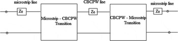
A 180° phase shifter for UWB applications is also proposed [Reference Eldek13]. The phase shifter is obtained using MP-CPW-MP transition using Rogers duroid 1060 with ε r = 10. Via holes are used to transfer the current from the top to the bottom substrate layer and vice versa. The phase shifter is operating in a wide bandwidth between 5.5 and 18 GHz, with low insertion loss and reflection coefficients. This concept leads to the design of MP–CBCPW–MP transition phase shifter using DGS, replacing via holes.A synthesize on cascaded multisection CBCPW–MP transition [Reference Costanzo14] has also analyzed to validate the design with its empirical relationship. The topology of the proposed design is depicted in Fig. 1.
Topology of the proposed model.

DGS have the characteristics of stop-band, slow-wave effect, and high impedance that has been created to reduce the harmonics as well as to realize the compact physical dimension of RF circuit. It minimizes the mutual coupling between microstrip and coplanar ground lines, which may then arise phase uncertainty. It also interrupts the shielded current distribution in the ground plane based on shape and dimension of the defect, resulting in controlled excitation and propagation of electromagnetic waves via the substrate layer. This characteristics has been utilized in the proposed phase-shifting technique to achieve desired phase.
Section II deals with the design and working of proposed phase shifter. In Section III, reflection coefficient, transmission coefficient, and phase shift are presented and analyzed. Finally, conclusion of the proposed work is highlighted in Section IV.
II. DESIGN AND WORKING
A MP–CBCPW–MP transition line with deployed DGS is designed to achieve desired phase. The microstrip and CPW sections are selected because of its low cost, compact size and easy integration of devices resulting in lower loss and compact transition. The CBCPW is a commonly used waveguide structure in planar printed circuits. CBCPW predominates here by choosing a ground plane width much smaller than λ/8 so that parallel plate and higher order modes can be avoided [Reference Costanzo14]. The transition between microstrip and CPW is achieved using electromagnetic coupling mechanism. The electromagnetic coupling is mostly advantageous by simply coupling the ground conductors or strip conductors. In this transition technique, the energy is transferred by coupling the fields from one mode into the fields of the other. This method provides inherent DC isolation between modes and requires no extra processing steps such as via holes or use of metal pads, providing efficient bandwidth of over 400 MHz.
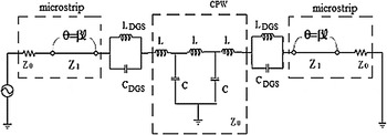
The working principle of the proposed phase shifter bounds with the resonance of both microstrip and DGS elements. As the DGS may induce radiation loss in the device, MP–CBCPW transition has been incorporated [Reference Shih and Itoh7]. The MP–CBCPW–MP transition yields high stability over the phase response of the device. The variation of phase characteristics due to DGS elements discussed in the literature [Reference Eldek13] reveal the linearity of phase in the presence of DGS. The equivalent circuit for the proposed system design is given in Fig. 2.
Equivalent circuit for the proposed phase shifter.

The equation relating characteristic impedance, impedance due to DGS and phase constant are given in Equation (1).
 $$\eqalign{{\theta _{21}} & = {\tan ^{ - 1}}\left\{ {\displaystyle{1 \over 2}\left( {\displaystyle{{{Z_1}} \over {{Z_0}}} - \displaystyle{{{Z_0}} \over {{Z_1}}}} \right)\displaystyle{{\sec 2\beta l} \over {2{Z_1} + \tan 2\beta l}}} \right. \cr &\, \left. \quad { + \displaystyle{1 \over 2}\left( {\displaystyle{{{Z_1}} \over {{Z_0}}} + \displaystyle{{{Z_0}} \over {{Z_1}}}} \right)\cot (2\beta l + {{\tan} ^{ - 1}}(2{Z_1}))} \right\},} $$
where θ 21 is the phase of the device, Z 0 is the characteristic impedance of the line, Z 1 is the transformed impedance due to the DGS element; β is the phase constant, and l is the length of the line.
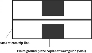
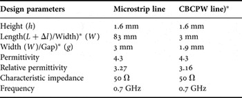
The design comprises with the analytical calculation over microstrip and CPW lines. The parameters taken in the design of microstrip and CBCPW lines are given in Table 1. The figure of the proposed phase shifter is shown in Fig. 3. The input is fed to microstrip line representing characteristic impedance of Z 0 = 50 Ω. The CPW center strip conductor width is also designed to bring consistency over the characteristic impedance of Z 0 = 50 Ω. The CPW center strip signal line length extends beyond the CPW ground plane by a distance ▵l to acquire CPW-microstrip transition.
MP–CPW–MP transition.

Dimension chart for the proposed prototype.

* refers to CBCPW parameter in specific.
Performance comparison of proposed structures at 0.7 GHz.

A quasi-transverse electro magnetic (TEM) approximation assumes that the lateral dimensions of the CPW have the condition as in (2)
 $$W + 2g \ll {\lambda _g}/2,$$
where W is the width of the signal line, g is the gap between signal and ground on both sides, and λ g is the guided wavelength. Hence, the parallel ground lines of CPW are of width and length 20 × 20 mm2.
The length of the coupled section of CPW is one-quarter wavelength in the three coupled microstrip sections at center frequency (f 0) of operation. CPW and microstrip taper lengths are typically 0.25 (λ/4) and 0.375 (λ/4), respectively. The two adjacent line lengths are made longer than the inner line length such that the electric fields between microstrip–coplanar–microstrip are equal in magnitude but 180° out of phase. The linear phase shift over CPW section is determined using Equation (3)
 $$\Delta \varphi = 2{f_0}\sqrt {{\varepsilon _{eff}}{\mu _{eff}}} \times l \times \displaystyle{{180} \over c},$$
where φ is the shift in phase, f 0 is the resonant frequency, ε eff and μ eff are the effective permittivity and permeability, l is length of the transmission line, and c is the velocity of light.
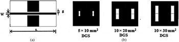
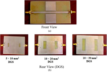
Hence, the phase shift occurs because of the permittivity of the region between the microstrip line and the ground plane as the air gap is introduced. The proposed structure with rectangular gap in the ground region of microstrip line, known as Defected Ground Structure is clearly depicted in Fig. 4.
MP–CPW–MP transition with defected ground. (a) Front view of the proposed model. (b) Rear view of the proposed model with pair of rectangular DGS.

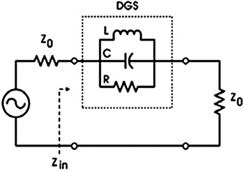
The equivalent circuit of rectangular DGS is given in Fig. 5. A pair of DGS present behind the adjacent microstrip lines are of 5 × 10, 10 × 20, and 10 × 30 mm2 size. The length L of the opening for a given geometry and substrate material is experimentally determined to achieve good impedance match with minimum insertion loss. However, the placement of DGS resonators along a transmission line introduces changes in the propagation of the wave along the line.
Equivalent circuit of rectangular DGS.

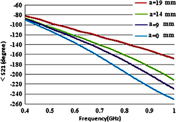
A parametric sweep has been simulated to analyze the effect of the width of opening of DGS, to validate its phase relationship. It has been given in Fig. 6.
Parametric sweep on the dimension of DGS width.

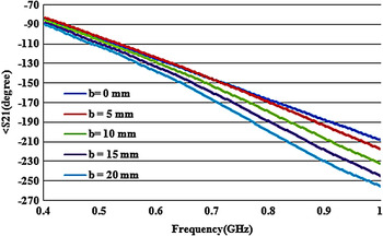
From the parametric sweep, it has been incorporated that increase in width of DGS increases the phase shift of the proposed transition transmission model. Moreover, the length of either one of the DGS element is varied to attain different dimension DGS pair configuration. The sensitivity of the configuration with its varying length is depicted in Fig. 7.
Geometric analysis on single DGS dimension.

From Fig. 7., it is incorporated that increase in length of DGS element also increases the shift in phase. Hence, phase shifters with different perimeter is selected for analyzing phase shift characteristics.
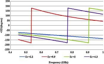
The proposed structure also contributes to change in phase with change in dielectric medium. The dielectrics namely, Rogers 5880, alumina, rubber, and FR4 epoxy glass are considered for analyzing phase characteristics of the proposed structure and given in Fig. 8.
Analysis of phase shift with different dielectric constants. (a) Front view. (b) Rear view (DGS).

From Fig. 8., it has been noted that there is linear proportionality exist between dielectric constant and phase shift satisfying Equations (1) and (2).
III. SIMULATION AND MEASUREMENT RESULTS
To validate the simulated results of the proposed design, the prototype is fabricated and measured. The simulation is performed in CST Microwave Studio and measured using Agilent Vector Network Analyzer E5062A, after performing Short Open Load Through (SOLT) method of calibration. The fabrication of phase shifter is simple and economical. Standard SMA Connectors are connected at both ends of the signal trace. The fabricated design is shown in Fig. 9.
Fabricated prototype model of MP–CPW–MP transition with DGS.

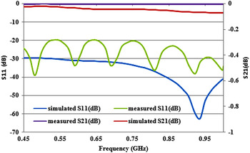
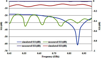
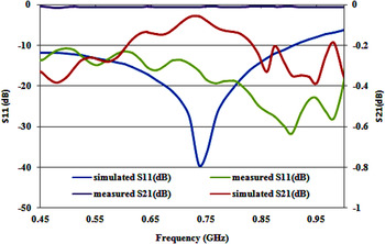
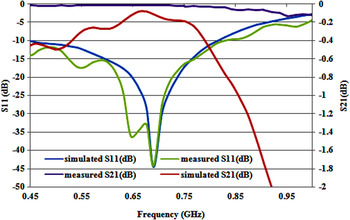
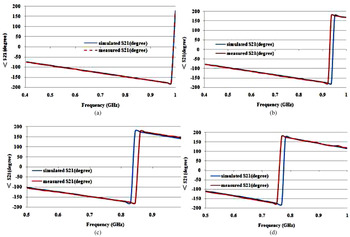
Figure 10 shows the simulated and measured results of reflection and transmission coefficients over the frequency band between 0.45 and 0.8 GHz of the proposed MP–CPW–MP transition model prototype without having DGS. Figures 11–13 show the simulated and measured results of reflection and transmission coefficients over the frequency band between 0.45 and 0.8 GHz of the proposed MP–CPW–MP transition model prototype with DGS of dimension 5 × 10, 10 × 20, and 10 × 30 mm2, respectively. Figure 14 shows the phase characteristics of the proposed prototypes. The phase delay for the proposed models are calculated by obtaining slope from the transmission phase results. From the phase slope values calculated, the fixed differential phase over the band is determined using Equation (4).
 $${\rm phasedelay} = \displaystyle{{{\rm phaseslope}\,({\rm ref}) - {\rm phaseslope}\,({\rm proposed})} \over {{\rm phaseslope}\,({\rm ref})}}.$$
Simulated and measured results of S 11 (dB) and S 21 (dB) for the proposed MP–CPW–MP transition model without DGS.

Simulated and measured results of S 11(dB) and S 21(dB) for the proposed MP–CPW–MP transition model with 5 × 10 mm2 DGS.

Simulated and measured results of S 11 (dB) and S 21 (dB) for the proposed MP–CPW–MP transition model with 10 × 20 mm2 DGS.

Simulated and measured results of S 11 (dB) and S 21 (dB) for the proposed MP–CPW–MP transition model with 10 × 30 mm2 DGS.

Simulated and measured S 21 (degree) for the proposed prototype with (a) no DGS, (b) 5 × 10 mm2 DGS, (c) 10 × 20 mm2 DGS, and (d) 10 × 30 mm2 DGS.

With DGS, perfect coupling is achieved to the transmission line using transition structure and perfect beam steering. It has been incorporated from the results that increase in dimension of DGS leads to increase in shift in phase. No vias or metal pads are used between the CPW adjacent ground planes and the finite fully coupled ground plane. The proposed MP–CPW–MP transition system is used to achieve stability over the system properties. The use of patterned copper foils over the substrate eliminates the need for high cost of film deposition or their processing in vacuum and/or clean room environment. The proposed structures have been designed for 0.7 GHz band andso the respective values of reflection coefficient and shift in phase values are tabulated in Table 2. The slope and phase delay values are calculated and presented in Table 2.
An increase in the dimension of DGS also decreases the resonance frequency. This has been negotiated with the effect of tight coupling in CPW signal line with the ground and the resonance characteristics is maintained by having a hold over the signal.
IV. CONCLUSION
A MP–CPW–MP transition analysis for phase-shifting application is performed . The proposed MP–CPW–MP transition system shows a gradual shift in phase when a gradual change in dimension of DGS is introduced. With the proposed prototype models, 5°, 20°, and 30° shift in phase are achieved with an acceptable range of reflection and transmission coefficients over the band. The negative slope values indicate the phase-lagging characteristics of the proposed model. Future work in this area may involve the change in center CPW signal line pattern and extending the transition to different substrates and frequency ranges to achieve different steering angles.
 Indhumathi Kulandhaisamy is currently pursuing her Ph.D. degree in the Department of Electronics and Communication Engineering, College of Engineering Guindy, Anna University, Chennai, India. Her area of interest includes Planar Microwave Devices.
 Malathi Kanagasabai is currently serving as an Associate Professor in the Department of Electronics and Communication Engineering, College of Engineering Guindy, Anna University, Chennai, India. Her research interests include Microwave Communication, Planar Transmission Lines, Planar Antennas, Signal Integrity Analysis in High-Speed Systems, etc.
 Dr. S. Indira Gandhi received Bachelor degree in Engineering from Madurai Kamaraj University. Post graduate degree and Ph.D. degree from Anna University in the faculty of Information and Communication. She is currently working as an Associate Professor in the Department of Electronics Engineering, MIT Campus, Anna University, Chennai, Tamil Nadu, India. Her research interest include Communication and Networking.
 Dr. Arun Kumar Shrivastav completed his Ph.D. degree from the Department of Electronics and Communication Engineering, Anna University, Chennai. He is currently working as Scientist F at Center for ElectroMagnetics, Society for Applied Microwave Electronics Engineering and Research (SAMEER), Chennai, India. His research interests include microwaves, transmission lines, antenna structures, and high-speed systems.
 M. Gulam Nabi Alsath obtained his B.E., M.E., and Ph.D. degrees from Anna University Chennai. Currently he is serving as an Associate Professor in the Department of Electronics and Communication Engineering, SSN College of Engineering, Chennai. He has published and presented his research articles in leading international journals and conferences. He is also reviewer for various Scientific and Engineering journals.