I. INTRODUCTION
Transparent conductive oxides (TCOs) based on doped zinc oxide have been used in many applications including optoelectronic devices, photovoltaic (PV) cells, and sensors.Reference Özgür, Alivov, Liu, Teke, Reshchikov, Dogan, Avrutin, Cho and Morkoç1–Reference Pandey and Tiwari6 The low cost of zinc, as compared to indium [in indium tin oxide (ITO films], and the increasing area of PV systems has been driving the increased demand for lower cost TCO films. In addition to the two-dimensional films, one-dimensional nanostructures, such as ZnO nanofibers (NFs), offer the advantage of a large surface-to-volume ratio as well as a conducting pathway along the fiber length. For sensor applications, a porous fiber structure would be optimal since the surface to volume ratio in such a fiber would increase, leading to increased potential sensitivity. Yet for ZnO fibers, the optimal way to form porous NFs has not been reported.
Different methods have been developed for the NFs fabrication,Reference Morales and Lieber7–Reference Marsen, Lonfat, Scheier and Sattler13 including the laser ablation metal catalytic vapor–liquid–solid method,Reference Morales and Lieber7–Reference Cui, Lauhon, Gudiksen, Wang and Lieber9 the oxide-assisted catalyst-free method,Reference Wang, Tang, Zhang, Lee, Bello and Lee10–Reference Gole, Stout, Rauch and Wang12 and solution techniques.Reference Holmes, Johnston, Doty and Korgel14 Nevertheless, the electrospinning technique, invented originally in 1934,Reference Formhals15 offers several advantages, including relative low cost and simplicity.Reference Li and Xia16, Reference Rutledge and Fridrikh17 NFs of many materials, including organic, ceramic, and metallic nature [e.g., Polyvinyl Alcohol (PVA), Polyethylene Glycol, Polylactic acid, TiO2, carbon–silver composite, and more], have been prepared by this technique. These NFs can be found in many applications such as membranes, catalysts, electronic devices.Reference Ramakrishna, Fujihara, Teo, Lim and Ma18–Reference Grader, Shter, Sonntag and Ricoux24
Ceramic and polymeric sensors can be found in varied applications. Ceramics have the advantage of long-term stability and functionality at high temperatures. Previous work described the use of zinc oxide as sensor for gases such as CO,Reference Lim, Hwang, Kim and Park25, Reference Ryu, Park, Akbar, Lee, Hong, Seo, Shin, Park and Choi26 C2H5OH,Reference Chen, Yan, Liu and Xue27, Reference Xiangfeng, Dongli, Djurišic and Leung28 H2,Reference Rout, Hari Krishna, Vivekchand, Govindaraj and Rao29 NO2,Reference Chen, Wang, Han, Gu and Guo30 and water vaporsReference Pandey and Tiwari6 by changes in the electrical resistivity. Doping with gallium improves the electrical conductivity by addition of charge carriers to the n-type ZnO.Reference Klingshirn2 Regarding humidity sensing, Kishimoto et al.Reference Kishimoto, Nakagawara, Seto, Koshido and Yoshino31 showed that addition of gallium improves the durability of ZnO films to humidity. Hong and ChungReference Hong and Chung32 showed that doping with ZnO thin films with gallium increases the sensitivity to humidity in mechanism of surface acoustic waves due to decrease in the particles size, hence increase in the surface area. Using a field-effect transistor (FET), the sensor sensitivity can be increased at an appropriate gate voltage region. For zinc oxide, this voltage region is located in the positive range due to its n-type semiconducting nature.
We report here that combination of Ga-doped ZnO (GZO), porous nanostructure with large surface area, and simplicity of fabrication facilitates a large potential in the field of gas sensing including humidity. This work describes the production of electrospun GZO NFs including the initial sol preparation, electrospinning process, and heat treatment in wide range of variable parameters. The morphological characterization and thermal stability of NFs mats were investigated. Optimal heat treatment with the minimal possible temperature and duration was developed to obtain zinc oxide NFs with stable fibrous structure. Moreover, the low sintering temperature leads to minimal zinc oxide particles with the largest surface area, which is advantageous for sensing applications
In one case, electrospun ZnO NFs were used in humidity sensing by making a paste from a large amount of NFs.Reference Wang, Li, Liu, Zhang, Zheng, Wang, Huang, Wang and Wang33, Reference Zhang, Li, Wang, Wang and Liu34 However, this group used pure ZnO, whereas the current study uses GZO, which has different properties. In summary, this paper reports for the first time the synthesis of GZO NFs by electrospinning, their sintering into a porous structure at a low temperature, and humidity sensing with a single GZO NF in a FET mode.
II. EXPERIMENTAL
A. Preparation of precursor solutions
GZO NFs were synthesized by electrospinning a solution of PVA/zinc salt followed by sintering in air.Reference Wu and Pan35, Reference Yang, Shao, Guan, Li and Gong36 The following starting materials were used: zinc acetate dihydrate [Zn(COOCH3)2•2H2O; Stream Chemicals, Boston, MA], gallium nitrate hydrate (Ga(NO3)3•H2O; Sigma-Aldrich, St. Louis, MO), and PVA (medium viscosity; City Chemical Corporation, West Haven, CT). The polymer to salt ratio was 1:2, and the solvents system included water (Milli-Q) and absolute Ethanol (Carlo Erba, Milano, Italy) in weight ratio of 60:40.
At first, a mixture of 30 g of water and 20 g of ethanol was prepared. Then, 4.4 g of PVA were added to yield an 8 wt% PVA solution. After 2.5 h of vigorous stirring at 70 °C, zinc acetate dihydrate was added in ratio of 2:1 to PVA (wt/wt) followed by an appropriate amount of gallium nitrate (2 wt% gallium/zinc). The mixture was stirred at 70 °C for 18 h until a homogeneous transparent solution was obtained. Finally, the solution was aged for 5 h at 60 °C before the electrospinning process.
B. Electrospinning
The electrospinning system included a high voltage supply, a syringe pump, and a grounded horizontal rotating collection disk. The precursor solution was fed through syringe needle at a rate of 0.3 ml/h. The distance between the needle and the collector was 12 cm, while the voltage between the needle and the collector was 15 kV.
C. Heat treatment
Fresh fibers were first dried under vacuum at 70 °C overnight to remove the solvents. After drying, the fibers were heated in two steps: (i) organics burnout and (ii) sintering. Optimal heat treatment conditions were based on thermal and phase analyses.
D. Analysis and characterization
Thermal analysis was done using simultaneous thermal gravimetric analysis/differential thermal analysis (TGA/DTA) (TG 92; Setaram, Caluire, France) in the room temperature (RT)—800 °C range, under airflow of 30 cc/min. Phase composition was determined by x-ray diffraction (XRD) measurement (powder diffractometer D5000; Siemens, Munich, Germany). Specific surface area was determined by Brunauer-Emmett-Teller (BET) single point measurement in the He/N2 flow (Monosorb, Quantachrome, FL). Morphology and structure were investigated by high-resolution scanning electron microscopy (ULTRA plus; Zeiss, Zurich, Switzerland).
E. Fabrication and characterization of FET based on ZnO/Ga NFs
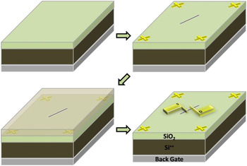
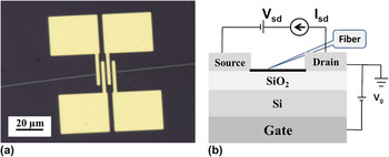
Fabrication of FET devices involved direct electrospinning of ZnO/Ga NFs on standard [001] silicon wafer coated with ∼100 nm SiO2 layer. Au/Ti electrodes were then deposited using electron beam lithography, evaporation, and liftoff (Fig. 1) in clean room facility. Before the device fabrication, the top SiO2 surface was slightly etched using oxygen plasma to remove any contamination followed by cleaning with ultrasonic treatment in acetone, methanol, isopropyl alcohol (IPA), and deionized water and drying with nitrogen. The electrodes were fabricated through a typical E-beam lithography process followed by electron beam evaporator of Ti/Au and finally a liftoff procedure using warm acetone and IPA. The gap between two adjacent electrodes was 2 μm. Electrical measurements were conducted using a semiconductor analyzer (Agilent B1500).
Scheme of electrodes deposition on single NF.

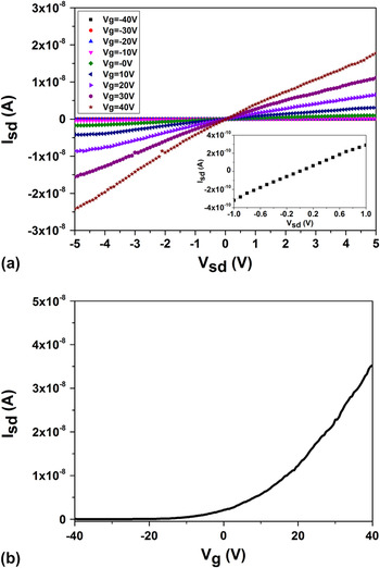
To assess the electrical characteristics of the ZnO/Ga NF FETs, two kinds of voltage-dependent back gate measurements were performed. In the first measurement, voltages between −40 and +40 V, in steps of 5 V, were applied to the degeneratively doped silicon substrate. For each gate voltage, the current–voltage (I–V) characteristics were measured between the two electrodes, i.e., between the drain (d) and source (s), contacted by a micromanipulator, at a bias range between −1 and +1 V, in steps of 50 mV, under ambient conditions. In the second measurement, voltages of 1 V were applied between the two electrodes and the current–back gate voltage (I–V g) measurements were made using a sweeping voltage from −40 V upward to +40 V, in steps of 200 mV, under ambient conditions.
The response of the ZnO/Ga NF FETs to various humidity levels was examined. For this purpose, a probe station that is connected to a device analyzer (Agilent B1500A) was used to collect the electrical signals of the ZnO/Ga NF FETs before and/or after exposure to humidity. Voltage-dependent back gate measurements (I ds−V gs), swept backward between +40 and −40 V with 200 mV steps and at 1 V source–drain voltage (V ds), were used to determine the performance of ZnO/Ga NF FET sensors.
III. RESULTS AND DISCUSSION
A. Characterization of zinc oxide NFs
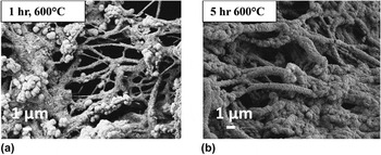
According to earlier work,Reference Yang, Shao, Guan, Li and Gong36–Reference Wang, Huang, Li, Zhang, Wang, Zheng and Wang39 the sintering time and temperature were >1 h at 600 °C in air. As shown in Figs. 2(a) and 2(b), we found that under these conditions, a significant amount of the NFs lost their fibrous structure. Hence, the sintering temperature and time were reduced to prevent these structural changes while reaching a complete burnout of the organic components.
Fiber morphology at elevated temperature: (a) 1 h at 600 °C, (b) 5 h at 600 °C.

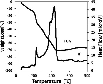
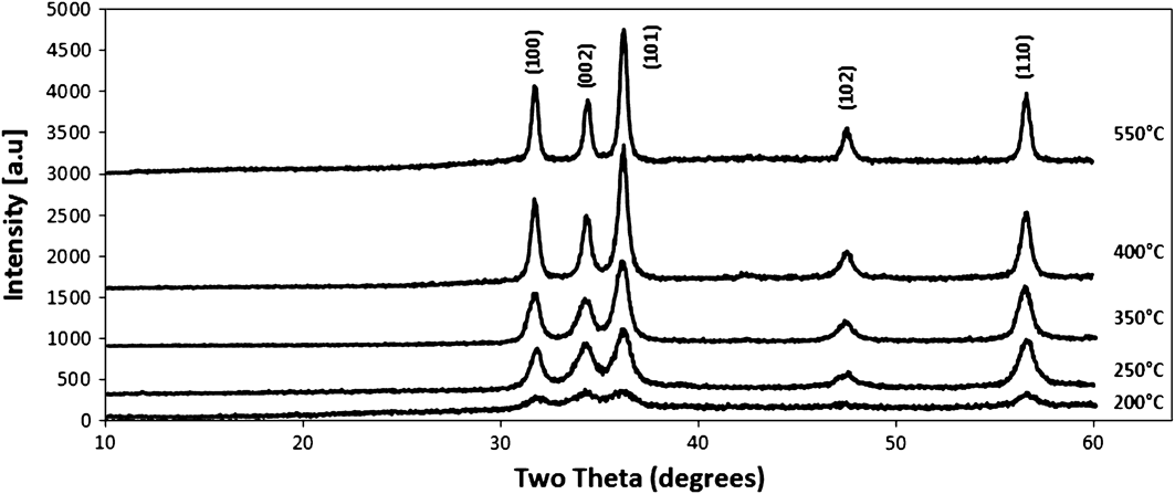
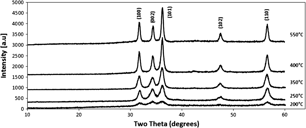
Thermal decomposition of the electrospun NFs is shown in Fig. 3. Exothermic peaks at 230, 380, and 410 °C occur due to oxidation and decomposition of the polymer (PVA) chains and the acetate groups. The total weight loss associated with organics burnout in the range of 200–490 °C was about 70% and that well matched with initial composition of electrospun solution. To determine the temperature range at which the ZnO phase forms, x-ray diffraction measurements were made on samples heated between 200 and 550 °C for 15 min. The resulting XRD patterns are shown in Fig. 4. It can be seen that the Zinc oxide phase is clearly present at 250 °C, although remnants of the peaks are evident even at 200 °C. The gallium doping level is too low to affect the ZnO XRD pattern. Analysis of the crystallite size based on Scherrer equation will be discussed below.
Thermal gravimetric (TG)/heat flow profile of “green” GZO NFs after electrospinning in air at heating rate of 5 °C/min.

X-ray pattern of GZO NFs after sintering at 200, 250, 350, 400, and 550 °C for 15 min.
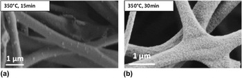
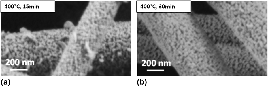
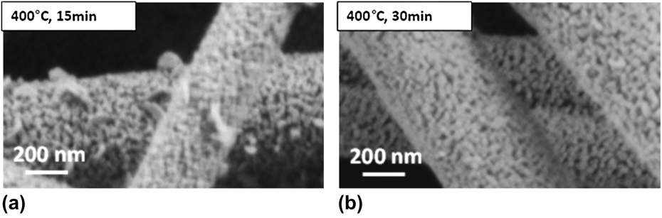
As mentioned earlier, the sintering at 600 °C for long duration leads to loss of the fiber structure as shown in Figs. 2(a) and 2(b). Therefore, fibers were sintered at the lowest possible temperature and shortest time that yielded a mechanically stable and uniform structure. Based on the TGA/DTA and XRD data in Figs. 3 and 4, the fibers were sintered at 350–400 °C for 15–30 min in a preheated oven. Figures 5 and 6 below show high resolution scanning electron microscopy (HRSEM) images of sintered fibers. At 350 °C, the fibers still includes a significant amount of organic matter consistent with the pattern in the TGA plot in Fig. 3. After 15 min at 350 °C, the fibers’ surface smooth [Fig. 5(a)]. After additional 15 min, some surface roughness appears on the fibers [Fig. 5(b)]; however, the underlying structure is nonporous. We propose that the organic residue fills the space between ceramic particles. The TGA data demonstrate a significant weight loss above 350 °C, which must be due to removal of this organic residue. In addition, this proposition is further supported by a strong charging of the samples prepared at 350 °C during HRSEM analysis due to limited conductivity. This charging prevented increasing the magnification beyond 30,000× during the measurements shown in Figs. 5(a) and 5(b). After 30 min at 400 °C, the said organic matter is removed, leading to a porous uniform fiber structure with well-connected nanoparticles in the range of 10–60 nm as shown in Fig. 6(b). This observation is well matched with TGA/DTA data (Fig. 3). The connectivity of the particles provided a conductive pathway that prevented charging during HRSEM analysis and allowed us to raise the magnification to 100,000× and 200,000× shown in Fig. 6 and Fig. 7(a), respectively.
HRSEM images of GZO NFs sintered at (a) 350 °C, 15 min (20,000×), (b) 350 °C, 30 min (30,000×).

HRSEM images of GZO NFs sintered at (a) 400 °C, 15 min (100,000×), (b) 400 °C, 30 min (100,000×).
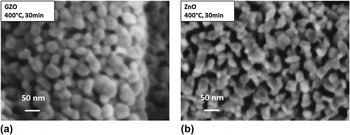
HRSEM images (200,000×) after sintering at 400 °C for 30 min of: (a) GZO NF, (b) pure ZnO NF.

The specific surface area of the fibers made at 400 °C and 30 min was 19.3 m2/g. Based on spherical ZnO particles and a theoretical density of 5.67 g/cm3, this area correlates with an average ZnO particle diameter of 55 nm. This diameter is in the range of the particles dimensions as seen in the HRSEM picture in Fig. 6(b) and Fig. 7(a) below.
The Scherrer equation was applied to the (101) peak in the XRD data shown in Fig. 4 to calculate the crystallite size. The crystallite size increases from 10 nm at 350 °C to 15 nm at 400 °C. This size is considerably smaller that the particle size observed by HRSEM [Fig. 7(a)] and calculated from the specific surface area above. This discrepancy may be attributed to small connected crystallites that appear as larger particles in the HRSEM figure.
Finally, in Fig. 7(b), the surface of an undoped ZnO fiber is shown at the same magnification as the GZO fiber in Fig. 7(a). As clearly seen, the porosity of the pure ZnO fiber is considerably larger than the doped fiber, and the particle shape and packing are different. While the morphology seen in the GZO case is a rounded particles, the morphology of the pure ZnO particles is elongated connected grains, which is consistent with the higher apparent porosity.
B. Conductivity and humidity sensing measurements
Devices with electrospun GZO NFs in a FET mode were fabricated and characterized as shown in Fig. 8. Drain current (I ds) versus drain–source voltage (V ds) curves of the GZO NFs were obtained by scanning a voltage range from −5 to +5 V at various gate voltages (V gs), as shown in Fig. 9(a). The two-terminal current versus drain–source voltage (I ds–V ds) curves were nearly linear through the origin, suggesting that the metal electrodes provided almost Ohmic contacts to the GZO NFs [see inset in Fig. 9(a)]. The curves also show typical accumulation mode of n-channel transistor behavior. The plot of I ds versus V gs [see Fig. 9(b)] at a constant V ds = 4 V shows a small current when the V gs is under a threshold voltage (V th). Furthermore, above V th, the I ds increases nearly linearly with V gs. Extrapolation of the linear region resulted in a V th of 15 V. The gate dependence of the curves confirmed the n-type nature of the GZO NFs. The slope in the linear region of I ds versus V gs gave a transconductance, g m = dI ds/dV gs, of ∼1.3 × 10⁻³ μS at V ds = 4 V. The transconductance obtained here was similar to that of FET devices fabricated from single ZnO nanowires prepared by chemical vapor deposition (CVD).Reference Fan, Wang, Chang, Tseng and Lu5, Reference Goldberger, Sirbuly, Law and Yang40 However, the transconductance of our GZO NFs was 104 larger than analogous ZnO NFs prepared by electrospinning elsewhere.Reference Wu, Lin, Zhang and Pan41 The observed source–drain current, I sd, at ±40 V was 10−12 to 10−8 A giving rise to an I on/I off ratio was about 104.
(a) Ti/Au electrodes deposited on a single GZO NF placed on Si/SiO2 wafer. (b) A schematic layout of the electrical measurement system.

Electrical behavior of single NF. (a) Source–drain current (I sd) versus source–drain voltage (V sd). (b) Source–drain current (I sd) versus gate voltage (V g).

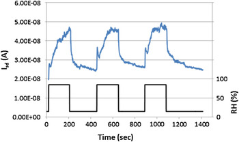
As seen in Fig. 10, the sensitivity of a single NF to humidity changes was measured by following the I sd, while the relative humidity (RH) surrounding the device was switched between 85% and 15%. Upon exposure to 85% RH, a sharp spike occurred in I sd, followed by an increase to a saturation level in about 60 s. Upon exposure back to 15% RH, the current decreased sharply to about half of the overall signal and then reached the average baseline level after 80 s. The NF showed stable cyclic behavior and consistency in its functionality.
Source–drain current (I sd) versus time during exposure to alternate relative humidities of 15% and 85%.

The change in the current due to the cyclic exposure to different RH% is not large in magnitudes but shows a high signal to noise ratio (>10:1). We expect an array of NFs fabricated into a device would yield a larger signal due to multiple contributions of the fibers in the sensing effect.
The sensitivity of the n-type GZO NFs to humidity changes is consequence of two mechanisms mentioned in the literature. The first is chemisorption of water vapor molecules on the large surface of the NFs. The water molecules dissociate on the surface and chemical reaction leads to formation of oxygen vacancies and transfer of free electrons to the zinc oxide. Accumulation of negative charge carriers in the n-type GZO lowers the resistance, hence the current increase. The additional mechanism is that at high values of RH, water is being condensed on the fibers surface and electrolytic conduction within the water is added.Reference Pandey and Tiwari6, Reference Jiang, Zhou, Zhang, Zhu, Li and Li42 The initial fast rise in current is probably due to the interaction with the outer surface of the fiber. The slower asymptotic change is likely to be due to diffusive effect into the fiber pores.
IV. SUMMARY AND CONCLUSIONS
In this work, GZO NFs were prepared by electrospinning of Zn salts/polymer solution. Based on thermal analysis of the green fibers, XRD data and morphology of final fibers, optimal firing temperature profile, and sintering conditions (400 °C for 30 min) were determined. The electrical properties of single GZO NF were tested for the first time using a FET device. The results showed behavior of n-type semiconductor. The measured transconductance of the nanowire was 1.3 × 10⁻³ μS. Extrapolation of the linear region in the I ds versus V g showed a threshold voltage, V th = 15 V. The open porosity and surface area of the fibers (19.3 m2/g) coupled to their n-type semiconducting nature render them as a potential sensor material. The response of the NFs to cyclic changes in humidity was demonstrated.
ACKNOWLEDGMENTS
The authors would like to thank the Grand Technion Energy Program, the Gruenbaum Chair in Materials Engineering, and joint grant from the Ministry of Absorption and the Council for Higher Education of Israel under the framework of the Kamea Program for support of this project. The authors would also like to thank TOTAL Co. for financial support of this project. Finally, we thank Dr. Michael Riesner for making the x-ray measurements.