I. INTRODUCTION
The efficiency of a thermoelectric material in converting waste heat into useful electrical energy is determined by its dimensionless figure of merit, ZT = S 2σT/κ, where S is the Seebeck coefficient, σ the electrical conductivity, and κ the thermal conductivity.Reference Uher1 CoSb3-based skutterudites exhibit reasonably good values of Seebeck coefficient and electrical conductivity and hence are promising thermoelectric materials.Reference Nolas, Morelli and Tritt2, Reference Tritt and Subramanian3 The complex crystal structure of CoSb3 offers a framework with voids that can be filled with guest ions, often called rattlers. If smaller sized atoms are used to fill the voids, they rattle about in the larger diameter voids. The loosely bound rattler atoms produce low-frequency local vibrational modes, effectively scattering the heat-carrying acoustic phonons and reducing the lattice thermal conductivity.Reference Nolas, Slack, Morelli, Tritt and Ehrlich4–Reference Yang, Wang, Iwasa, Kohgi, Sugawara and Sato7 The double filling approach wherein two different ions of varying masses are used to fill the voids has attracted an increased attention in recent years since this approach can effectively extend the range of the phonon spectrum that can be attacked.Reference Peng, He, Alboni and Tritt8–Reference Zhao, Dong, Wei, Guan, Liu, Zhai, Tang and Zhang10 In- and Yb-filled CoSb3 crystals have been reported to have ZT of unity at high temperatures, a benchmark criterion for effective conversion of thermal energy into electricity.Reference Peng, He, Alboni and Tritt8, Reference Peng, Alboni, He, Zhang, Su, Holgate, Gothard and Tritt9, Reference Peng, He, Su, Alboni, Zhu and Tritt11 Recently, there has been some debate as to whether In occupies the cages as a rattler atom or dopes with Sb in the system.Reference Graff, Zhu, Holgate, Peng, He and Tritt12
Further reduction in thermal conductivity is possible by preparing skutterudites in the form of low-dimensional systems such as thin films.Reference Durand, Nishimoto, Ito and Kataoka13, Reference Song, Liu, Zeng, Borca-Tasciuc, Chen, Caylor and Sands14 The presence of grains and grain boundaries in thin films can serve as additional scattering centers and help reduce the thermal conductivity. However, skutterudite thin films have been reported to have inferior power factor (S 2σT) compared with their bulk counterparts, negating the possible improvement of ZT by the reduction of thermal conductivity.Reference Durand, Nishimoto, Ito and Kataoka13, Reference Zeipl, Walachova, Lorincik, Leshkov, Josiekova, Jelinek, Kocourek, Jurek, Navratil, Benes and Plechacek15, Reference Savchuk, Schumann, Schupp, Behr, Mattern and Souptel16 The difference in behavior of the material in bulk and thin film forms is believed to be the major reason behind the failure of efforts to enhance ZT. Furthermore, skutterudite films have a very narrow range of stability, and deviations from the optimal deposition conditions result in off-stoichiometric or multiphase regions resulting in deterioration of the thermoelectric properties.Reference Caylor, Stacy, Gronsky and Sands17
Direct current (dc) and radio-frequency (rf) magnetron sputtering,Reference Savchuk, Schumann, Schupp, Behr, Mattern and Souptel16, Reference Arnache, Girata, Perez, Castro, Prieto and Lopera18–Reference Schupp, Bacher, Hecker, Mattern, Savchuk and Schumann20 co-evaporation of constituent elements,Reference Hornbostel, Hyer, Edvalson and Johnson21–Reference Sellinschegg, Stuckmeyer, Hornbostel and Johnson23 and pulsed laser deposition (PLD)Reference Durand, Nishimoto, Ito and Kataoka13, Reference Zeipl, Walachova, Lorincik, Leshkov, Josiekova, Jelinek, Kocourek, Jurek, Navratil, Benes and Plechacek15, Reference Caylor, Stacy, Gronsky and Sands17, Reference Colceag, Dauscher, Lenoir, Da Ros, Birjega, Moldovan and Dinescu24, Reference Caylor, Sander, Stacy, Harper, Gronsky and Sands25 are the three prominent methods reported for the growth of skutterudite films. Though CoSb3 films have been explored in much detail in previous works, filled CoSb3 thin films have not been extensively studied. A better understanding of the structure–property relations in doped CoSb3 thin films is valuable for the realization of high-efficiency materials for diverse applications. In the present work, we report the thermoelectric properties of CoSb3 thin films with In and Yb deposited by PLD under different conditions. The target materials were grown under typical conditions for these materials, but the materials were ground into powders before employing a spark plasma sintering to make a dense PLD target. The optimized growth conditions for obtaining single-phase films are identified, and the effect of postgrowth annealing in argon on the thermoelectric properties of the single-phase films is discussed.
II. EXPERIMENTAL
The PLD growth chamber (Neocera, Beltsville, MD) used for the depositions was evacuated to an ultrahigh vacuum (<10−7 Torr) prior to the deposition. A spark plasma sintered In0.2Yb0.2Co4Sb12 target was used for the ablation. The details of the synthesis of the target can be found elsewhere.Reference Peng, Alboni, He, Zhang, Su, Holgate, Gothard and Tritt9 When appropriate, process gas (high-purity argon) was introduced into the chamber using a mass flow controller, and the process gas pressure was maintained at predetermined values (10, 20, and 100 mTorr). Films were also deposited under ultrahigh vacuum conditions (denoted as 0 mTorr). A KrF (248 nm) excimer laser (Compex Pro 205, Coherent, Santa Clara, CA) with pulse duration of 20 ns and a repetition rate of 10 Hz was used for ablation of the target, which was held in a rotating carousel to enable uniform ablation of the target surface. The incident angle of the laser with respect to the target was ∼45°. The fused quartz substrates (10 × 10 mm2) were mounted using silver paste on a rotating substrate holder held above the target. A radiation heater arrangement helped to maintain predetermined substrate temperatures (250, 260, 270, and 280 °C) during deposition. The target-to-substrate distance was held fixed at 9 cm. A laser fluence of 200–230 mJ pulse−1 (4–4.6 J cm−2) was used for the ablation of the target. The thickness of the films was kept constant at ∼190 nm as measured using a stylus profilometer (Dektak 150) and cross-sectional scanning electron microscope (XSEM, Helios Nanolab 400s, FEI, Hillsboro, OR).
The influence of substrate temperature, process gas pressure, and post-deposition heat treatments (in argon ambient) on the phase purity and thermoelectric properties of the films was analyzed. All films were characterized by grazing-incidence x-ray diffraction (GIXRD, D8 Discover, Bruker AXS, Karlsruhe, Germany) to determine the phase purity, high-resolution transmission electron microscopy (HRTEM, FEI Titan 80-300 kV (ST)) to characterize the microstructure, and atomic force microscopy (AFM, MP3D-SA, Asylum Research, Santa Barbara, CA) to assess the surface morphology. The composition of the films was estimated using energy dispersive x-ray analysis (EDAX). Electrical resistivity and Seebeck coefficient of the films were measured in the temperature range 300–700 K in argon ambient, respectively, using the linear four-probe and differential methods, employing a Seebeck tester (RZ2001i, Ozawa Science Co Ltd., Nagoya, Japan). The measurements were repeated to identify any changes in the high-temperature thermoelectric properties of the films subjected to different cycles of heating, each time cooling the film to room temperature. Each of the measurement cycles took 14 h to complete, and hence the films may be considered to have undergone annealing in argon ambient.
III. RESULTS AND DISCUSSION
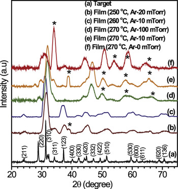
The GIXRD of the films grown under different deposition conditions on fused quartz substrates are shown in Fig. 1, along with the powder diffraction pattern of the target. It is clearly seen that the films are polycrystalline in nature. Films formed at a substrate temperature of 260 °C and argon pressure of 10 mTorr did not show any secondary phases or segregation of the volatile Sb within the resolution limit of GIXRD. However, the possibility of the dopant atoms occupying the lattice sites rather than the cages cannot be ruled out in our films. Hence, the films are better described as In- and Yb-doped (rather than “filled”) CoSb3 films. The formation of single-phase films was not found to depend on the energy density of the laser within the range 4–4.6 J cm−2. The composition of the single-phase films was found to be the same as that of the nominal target composition within the error limit of EDAX. CoSb2 second phases were observed for films grown at other deposition conditions and are marked with an asterisk in Fig. 1. In these films, the highest intensity peak is found to shift toward lower d values due to the presence of CoSb2 secondary phases. It is to be noted here that the d values corresponding to the highest intensity peak for CoSb3 and CoSb2 phases are 2.85 and 2.77 Å, respectively.
X-ray diffraction pattern of the In0.2Yb0.2Co4Sb12 target and grazing-incidence x-ray diffraction patterns for the films deposited on fused quartz substrates under different substrate temperatures and argon pressures. The indexing is based on the CoSb3 structure. The CoSb2 phases in the films are indicated by asterisk.

The substrate temperature and background gas pressure have been reported to play a significant role in the phase-purity of the skutterudite films.Reference Caylor, Stacy, Gronsky and Sands17, Reference Colceag, Dauscher, Lenoir, Da Ros, Birjega, Moldovan and Dinescu24, Reference Caylor, Sander, Stacy, Harper, Gronsky and Sands25 Sb-deficient CoSb2 secondary phases have been reported to be present in CoSb3 films grown at a substrate temperature above 250 °C.Reference Colceag, Dauscher, Lenoir, Da Ros, Birjega, Moldovan and Dinescu24 The stoichiometric flux of Co and Sb is reported to be insufficient for the formation of the skutterudite phase due to the high volatility of Sb. Excess Sb is usually added to compensate for the loss and increase the temperature range over which single-phase films can exist. In the present work, however, no excess Sb was required even at a substrate temperature of 260 °C. The presence of inert gas background is another factor that affects the formation of single-phase films. The background inert gas pressure helps lower the flux as well as energy of the ablated species, thereby lowering the internal stress of the films. The large target-to-substrate distance (9 cm) and the presence of inert gas ambient ensured that all the films were free of blistering, which is a common problem in skutterudites films grown by PLD.
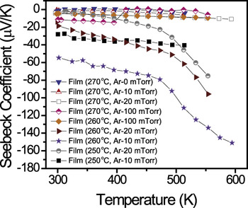
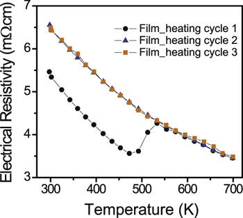
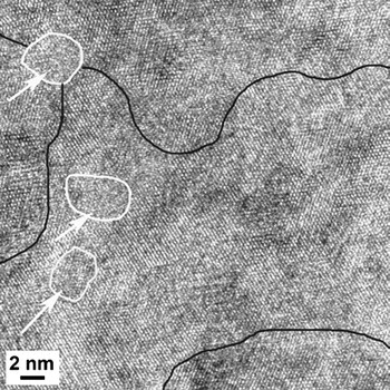
The films having prominent secondary phases showed slightly lower resistivity values compared with the single-phase films. However, the absolute values of the Seebeck coefficients of the multiphase films were significantly lower than that of the single-phase film as shown in Fig. 2. It is to be noted here that the presence of CoSb2 and other secondary phases degrade the thermoelectric properties of the bulk material as well.Reference Zhao, Tian, Liu, Zhan and Chen26 Hence, for further studies, the single-phase films (grown at 260 °C and 10 mTorr of Ar) were used. The temperature dependence of resistivity of the single-phase films for different heating cycles in argon ambient is shown in Fig. 3. It is evident that the film grown under optimal conditions is semiconducting in nature. This is in sharp contrast to the metallic or degenerate semiconductor behavior exhibited by the bulk material.Reference Peng, He, Su, Alboni, Zhu and Tritt11, Reference Graff, Zhu, Holgate, Peng, He and Tritt12 Similar semiconducting behavior has been reported for undoped CoSb3 films. Moreover, the resistivity of the films is higher than that obtained for the bulk material. For instance, the resistivity of the as-deposited film at 300 K is 6.5 mΩ cm, while the corresponding value for the bulk is only 0.6 mΩ cm.Reference Peng, He, Su, Alboni, Zhu and Tritt11 The higher resistivity of the films may be due to the polycrystalline structure with a high concentration of grain boundaries as evidenced in the HRTEM image shown in Fig. 4. The typical grain size in the films was in the range 20–50 nm as compared with the large grain size in the bulk (1–10 μm).Reference Peng, Alboni, He, Zhang, Su, Holgate, Gothard and Tritt9 The high concentration of structural defects in the films results in a high potential barrier for the conduction electrons, thereby reducing the mobility of the charge carriers and hence the electrical conductivity. Additional point defects and surface defects also arise due to the presence of grain boundaries that enhance the scattering effects. A sharp irreversible increase in the resistivity of the film is observed in the first heating cycle in the temperature range 480–530 K. After 530 K, the film again shows the semiconducting behavior up to 700 K but with a higher resistivity. The temperature dependence of resistivity remained unchanged for all the subsequent heating cycles and no abrupt changes in resistivity were observed. However, the absolute value of resistivity at any given temperature increased after the first heating cycle. The composition of the film before and after the heating cycles remained the same. The films were completely destroyed if heated beyond 750 K due to the evaporation of the highly volatile Sb making it impossible to measure the properties of the films at temperatures around 800 K wherein the bulk material showed a maximum ZT of ∼1.2. Though there has been no report on the thermal degradation of the doped bulk material, thermal degradation in inert ambient (He) is reported to start at around 693 K in bulk undoped CoSb3 wherein the volatile product of the decomposition is identified as elemental Sb.Reference Leszczynski, Wojciechowski and Malecki27 Recently, protective coatings have been reported to be effective in preventing the decomposition of bulk skutterudites at elevated temperatures.Reference Godlewska, Zawadzka, Mars, Mania, Wojciechowski and Opoka28
Seebeck coefficient of the as-grown films as a function of temperature. The data for the single-phase film is shown as filled stars.

Temperature dependence of electrical resistivity of the films as a function of heating cycle.

High-resolution transmission electron microscopy image of as-deposited In0.2Yb0.2Co4Sb12 films. Tiny amorphous regions embedded in the polycrystalline matrix are shown by the bounded regions in white, pointed by the arrows.

A similar sharp increase in resistivity during the first heating cycle has been reported for Fe-doped CoSb3 amorphous films grown by sputtering, which was attributed to the phase transition from amorphous to the crystalline state.Reference Savchuk, Boulouz, Chakraborty, Schumann and Vinzelberg19 The HRTEM image of certain regions of the films shows the presence of tiny (∼4 nm) amorphous regions between the crystallites as indicated by the bounded white regions indicated by arrows in Fig. 4. Hence, the observed irreversible increase in resistivity may be explained based on the possible crystallization of amorphous regions in the film upon heating. However, the possible crystallization of the small concentration of amorphous phases in the otherwise single-phase matrix may not be sufficient to cause the observed abrupt change in resistivity. Moreover, HRTEM analysis of the annealed films also revealed scarcely distributed amorphous phases in certain regions, ruling out the possible explanation based on crystallization.
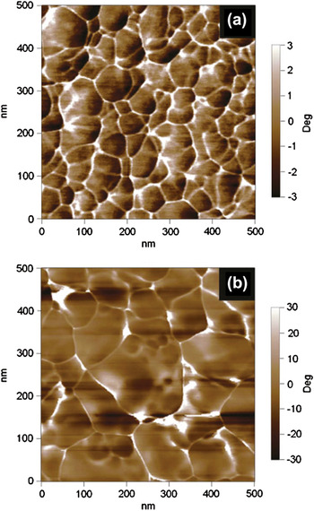
Surface roughness is another parameter that plays a major role in determining the resistivity of thin films.Reference Ke, Zahid, Timoshevskii, Xia, Gall and Guo29 It is well established that the enhanced scattering of charge carriers at the surface can result in an increase in the resistivity of rough metallic and semiconducting films.Reference Hakiki30, Reference Marom and Eizenberg31 The AFM phase-retrace images of the films before (as-deposited) and after the first heating cycle are shown in Figs. 5(a) and 5(b), respectively. It is evident that the surface morphology of the films changes drastically upon annealing. The rms surface roughness is found to increase from 3 to 14 nm upon the first heating cycle and remained practically the same after the subsequent heating cycles. The enhanced surface roughness may be one of the reasons behind the irreversible increase in resistivity of the film after the first heating cycle.
Atomic force microscopy phase-retrace images of the film (a) before (as-deposited) and (b) after the first heating cycle.

Another possible explanation for the observed effects is the formation of CoSb3 phase at the expense of CoSb2 phase. It has been reported that the nanostructured CoSb3 forms at nearly 250 °C (523 K) through the formation of intermediate CoSb2.Reference Mi, Zhao, Zhu, Tu and Cao32 The presence of secondary CoSb2 phases in our optimized films cannot be completely ruled out as their presence may be below the detection limit of the GIXRD. It was observed that the films with obvious secondary phases show much lower Seebeck coefficient (Fig. 2) and higher electrical conductivity, while the optimized film shows improved Seebeck coefficient and lower conductivity. The observed effects can then be fully explained if we assume the presence of traces of CoSb2 and Sb secondary phases which are beyond the detection limit of GIXRD in the optimized as-deposited films. When heated to ∼523 K and above, these trace secondary phases react to form the CoSb3 phase, thereby increasing the resistivity and the Seebeck coefficient. It is to be noted that the slope of the resistivity and Seebeck coefficient curves changes at around 500 K during the first heating cycle, which supports the aforementioned explanation.
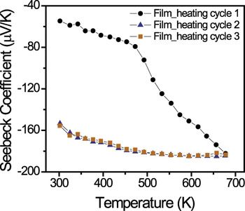
The variation of Seebeck coefficient with temperature of the film for the different heating cycles is shown in Fig. 6. The Seebeck coefficient of the films was negative indicating n-type conduction. During the first heating cycle, the absolute value of Seebeck coefficient (S) increased abruptly at ∼480 K, the same temperature at which the resistivity changed irreversibly. The temperature dependence of S remains unchanged for all the subsequent heating cycles, wherein the maximum temperature was limited to 700 K. The highest value of Seebeck coefficient obtained was −185 μV K−1, which is lower than the maximum value obtained for the bulk (−208 μV K−1) at the same temperature (603 K).
Variation of the Seebeck coefficient of the films with temperature as a function of heating cycle.

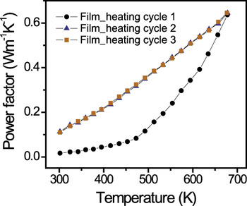
The temperature dependence of the power factor for the heating cycles is shown in Fig. 7. The obtained power factor values were reproducible, once the films were subjected to the initial heat treatment up to 700 K. The obtained maximum power factor of 0.68 W m−1 K−1 at ∼700 K is nearly six times lower than that of the bulk material, mainly due to the enhanced resistivity of the films. PLD-deposited n-type Yb0.14Co4Sb12 and p-type Ce0.09Fe0.09Co3.33Sb12 have been reported to have similar inferior power factor values compared with their bulk counterparts.Reference Zeipl, Walachova, Lorincik, Leshkov, Josiekova, Jelinek, Kocourek, Jurek, Navratil, Benes and Plechacek15 The presence of secondary phases, low Hall mobility, and large resisitivity of the polycrystalline films have been reported to be the major reason for the inferior power factor exhibited by sputtered CoSb3 films.Reference Savchuk, Boulouz, Chakraborty, Schumann and Vinzelberg19 The results suggest that a higher resistivity should be expected in polycrystalline films of skutterudites, even if the films are single-phase in nature. However, the increase in resistivity is expected to bring in a corresponding decrease in the thermal conductivity. Although the thermal conductivity of thin films is expected to be significantly lower compared to the bulk, future direct measurements of thermal conductivity of the films are required to draw a conclusion on the potentials of In0.2Yb0.2Co4Sb12 films as thermoelectric materials.
Temperature variation of the calculated power factor of the films with different heating cycles.

IV. CONCLUSION
Polycrystalline CoSb3 skutterudite films doped with In and Yb were successfully prepared using PLD despite an extremely narrow process window. The Seebeck coefficient and electrical resistivity of the films varied drastically with phase purity of the films. An increase in surface roughness of the films is observed after the first heating cycle in argon ambient. The possible formation of CoSb3 phase at the expense of trace secondary phases together with the enhancement in surface roughness upon the first heating cycle is invoked to explain the irreversible change in the resistivity and Seebeck coefficient of the films at 480 K. The films exhibited repeatable thermoelectric properties after heating up to 700 K. The highest power factor of 0.68 W m−1 K−1 obtained at ∼700 K is five times lower than that reported for the bulk. The inferior power factor resulting from the high electrical resistivity of the films was due to the polycrystalline nature of the films with high concentration of grain boundaries.
ACKNOWLEDGMENTS
HA acknowledges the baseline funding from King Abdallah University of Science and Technology (KAUST) and the faculty initiated collaboration fund (FIC) grant. T.M. Tritt would like to acknowledge the financial support from Department of Energy/Experimental Program to Stimulate Competitive Research (DOE/EPSCoR) Implementation Grant No. (DE-FG02-04ER-46139) for the work at Clemson.