Introduction
The rapid evolution of wireless communication necessitates robust advancements in radio frequency and microwave technologies to meet the escalating demands for high data rates, spectral efficiency, and reliable connectivity. In this context, the design and optimization of microwave multiplexers are paramount, as these components are critical for signal separation and combination in multiband systems. While numerous design techniques have been reported [Reference Song, Zhou, Chen, Patience, Guo and Fan1]–[Reference Ben Haddi, Zugari, Zakriti, Yahya and L24], achieving a balance between compactness, isolation, and fabrication simplicity remains a significant challenge. Among the various design methodologies, Defected Ground Structure technology has attracted considerable attention, as evidenced by the designs reported in [Reference Song, Zhou, Chen, Patience, Guo and Fan1, Reference Deng, Lei, Lo and Li2]. These designs achieve excellent frequency isolation and low passband insertion losses, though they come with some complexities. In [Reference Loi, Ha, Hieu and Manh3], a Complementary Split Ring Resonator (CSRR)-based Substrate Integration Waveguide (SIW) triplexer offering low-loss performance, wide passband ratio, and compactness at 6, 8, and 10 GHz, with good agreement between simulations and measurements; however, the large circuit size remains a disadvantage of the proposed design. Additionally, [Reference Yahya, Zubir, Hafez, Nkenyereye, Chaudhary, Assaad, Nouri, Rezaei and Jizat4] proposes a microstrip triplexer for mid-band 5G. However, the overall electrical performance of the proposed design remains a notable limitation. Other notable methods include loop resonators with feed coupling using lumped capacitors [Reference Yahya, Zubir, Hafez, Nkenyereye, Chaudhary, Assaad, Nouri, Rezaei and Jizat4] and substrate-integrated suspended line technology [Reference Gorur and Karpuz5]. Each approach has its own advantages and challenges, offering specialized solutions to meet specific design needs. Multiplexer designs are presented in [Reference Chu, Kaixue and Wang6, Reference Xu, Wan, Ding and Zhu7] using distributed resonators and coupled filters. While the triplexer presented in [Reference Keshavarz, Abdipour, Mohammadi and Keshavarz8] is designed using L-type matching networks, compact size and enhanced selectivity pose challenges. Another method to design a planar four-port microstrip triplexer is to use spiral cells and compact patches for wireless communication applications [Reference Yang and Rebeiz9]. In [Reference Rezaei, Yahya, Moradi and Jamaluddin10], a sophisticated coupling structure with short-circuited resonators is used to design a four-port triplexer. This configuration is designed to achieve higher levels of isolation; however, the circuit size remains an issue. A high-performance triplexer is developed in [Reference Mohammadi, Ebadzadeh and Mohammadifar13], employing a low-pass filter. This design offers enhanced electrical performance in terms of isolation and signal rejection. Moreover, [Reference Chen, Liu and Shi14] presents the design using step impedance resonators for simplified matching. This approach offers potential advantages; it also highlights challenges caused by undesirable spurious resonances. Additionally, [Reference Chen, Zhang and Shi15] introduces a design incorporating the hairpin resonators, comprising three hairpin bandpass filters (BPFs) and a T-shaped microstrip line for signal division. However, the inherent complexity of these designs must pose challenges. To address these limitations, this work introduces a high-isolation quad-port microstrip triplexer featuring a modified step-impedance coupled-line (MSICL) resonator for the third band. In contrast, the exploration of triplexer designs based on the principles of multimode interference (MMI) couplers, as exemplified in [Reference Wang, Huangfu and Chen20]–[Reference Idrees, Khalid, Rehman, Ullah, Hussain and Iqbal27], has generated considerable interest. [Reference Khani, Danaie, Rezaei and Shahzadi28] presents a compact octagonal microstrip triplexer operating at 3.5, 5, and 6 GHz with low insertion loss, high isolation, and excellent return loss, making it a strong candidate for 5G, Wi-Fi, and satellite applications. Despite advancements in microstrip triplexer design, challenges persist in achieving a balance between compact size, low insertion loss, and high isolation. Existing designs often involve complex structures that increase fabrication costs. Moreover, bandwidth flexibility remains a concern, restricting their application in multiband wireless systems. Further research is needed to develop miniaturized, high-performance triplexers with enhanced impedance matching and seamless integration into emerging technologies like 5G and IoT.
Unlike conventional triplexers that rely on complex matching networks or bulky resonator layouts to achieve isolation, this work introduces an MSICL resonator for the third band. This specific topology incorporates asymmetric open- and short-circuited stubs within the coupling structure itself. This allows for independent control of transmission poles and transmission zeros, resulting in superior isolation and compactness (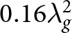 $0.16 \lambda_g^2$) without the need for external matching circuits. The triplexer operates at center frequencies of 1.20, 2.88, and 4.45 GHz, achieving fractional bandwidths (FBWs) of 33.3
 $\%$, 30.2
 $\%$, and 22
 $\%$, respectively. Measurement results demonstrate an in-band return loss exceeding 12.3 dB and an insertion loss lower than 0.63 dB across all channels. The fabricated prototype exhibits strong alignment with electromagnetic simulations, confirming design robustness. With its competitive performance metrics and compact form factor, this triplexer emerges as a viable solution for advanced applications in next-generation networks and IoT-enabled wireless communication systems.
Design methodology
Synthesis procedure
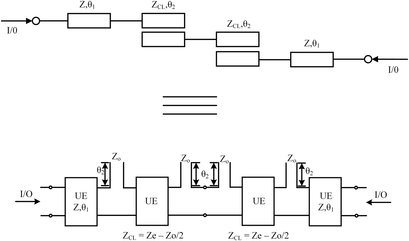
This paper presents the new design of a four-port triplexer incorporating a modified coupled line resonator to achieve high isolation among adjacent frequency bands, as shown in Figure 1. The proposed triplexer is composed of three isolated BPFs, where filters 1 and 2 utilize identical coupled-line structures with different physical parameters, and filter 3 is realized using a novel coupled-line configuration. Figure 1 illustrates the schematic model of filter 1, while eq. 1 represents its transfer matrix. The structure shown in Figure 1 consists of two parallel coupled lines interconnected with transmission lines.
Schematic of  $BPF_1$ with its equivalent circuit model.

 \begin{align}
[T_1] &= \prod\limits_{q = 1}^{2}\left[ \begin{array}{*{20}{c}}
{\cos ({\theta})}&{j{Z_c}\sin ({\theta})}\\
{\frac{{j\sin ({\theta})}}{{{Z_c}}}}&{\cos ({\theta})}
\end{array} \right]
\times \prod\limits_{q = 1}^{4} {\left[ {\begin{array}{*{20}{c}}
1&{\frac{{- j{Z_o}}}{{\tan (\theta )}}}\\
0&1
\end{array}} \right]} \nonumber\\
&\quad \times \prod\limits_{q = 1}^{2}\left[ {\begin{array}{*{20}{c}}
{\cos ({\theta})}&{j{Z}\sin ({\theta})}\\
{\frac{{j\sin ({\theta})}}{{{Z}}}}&{\cos ({\theta})}
\end{array}} \right]
\end{align}
where  $Z_{CL}$ is the impedance of the coupled line and
 $Z_o$ is the impedance of the open circuit stub, while
 $Z$ is the impedance of the transmission line. After determining the transfer function using eq. 1, the transmission coefficient
 $S_{21}$ is calculated using the known relationship illustrated in eq. 2. The transfer function is derived using the ABCD matrix method. The even-mode (
 $Z_e$) and odd-mode (
 $Z_o$) impedances determine the coupling strength. From the transmission coefficient
 $S_{21}$, the filtering function can be extracted using eq. 3.
 \begin{equation}
{S_{21}} = \frac{2}{{A + B + C + D}}
\end{equation}
 \begin{equation}
{\left| {{S_{21}}(j\omega )} \right|^2} = \frac{1}{{1 + {\varepsilon ^2}G_N^2(\theta )}}
\end{equation}
Here,  $G_N(\omega)$ indicates the filtering function of the
 $N_{th}$ order, and
 $\varepsilon ^2$ is the ripple level. The derived filtering function of the proposed filter is of order (N = 8). The electrical parameters were derived by applying Chebyshev Type 1 polynomials to the filtering function. Addressing the frequency-dependent terms in both the numerator and denominator of the filtering function required precise determination of these parameters. To mitigate the influence of the frequency-dependent component, the analytical approach outlined in reference [Reference Hunter29] was adopted, ensuring robust compensation for its effects.
 \begin{equation}
{G_8}(\theta ) = \frac{{\alpha {{\cos }^8}(\theta ) - \beta {{\cos }^6}(\theta ) + \gamma{{\cos }^4}(\theta ) - \zeta{{\cos }^2}(\theta )}}{{{{\tan }^2}(\theta )}}
\end{equation}
Here  $\alpha, \beta, \gamma$, and
 $\zeta$, derived from Chebyshev polynomials, are complex filtering coefficients. The filtering coefficient equations, given in Appendix, are a function of the characteristic impedance of the design topology. The electrical parameters of
 $BPF_1$ are calculated as
 $Z = 35.45$
 $\Omega$,
 $Z_{o}=61.04$
 $\Omega$,
 $Z_{e}=129.9$
 $\Omega$, and
 $\theta = 90^o$. The summary of the synthesis process, which started from channel specification, transfer matrix derivation, filter validation, channel combining, EM simulation, and fabrication, is given in Appendix.
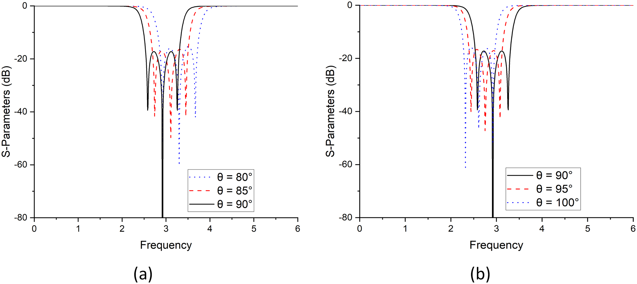
In the given configuration, the  $BPF_1$ provides a bandpass response at 2.88 GHz with three transmission poles. Figure 2 shows the relationship between electrical length and
 $\theta$ for
 $BPF_1$. As the electrical length increases, the center frequency of the first passband shifts to a lower frequency. Conversely, decreasing the length causes the center frequency to shift to a higher frequency.
Frequency response of  $BPF_1$ with variable electrical length.

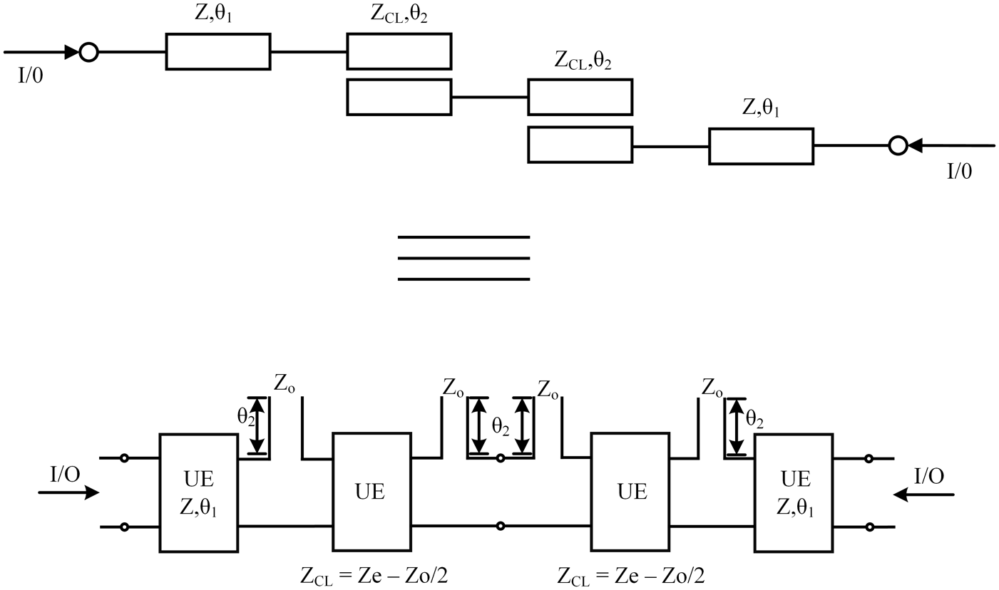
Figure 3 shows a second BPF ( $BPF_2$) with its equivalent circuit model. The
 $BPF_2$ has the same configuration as
 $BPF_1$ but with different electrical parameters. The filtering function of
 $BPF_2$ is derived in the same way as for eq. 4 but for different frequencies. The parameters for
 $BPF_2$ are Z=35.61,
 $Z_o$=104.02,
 $Z_e$=170.23 ohm, and
 $\theta= 90^o$. In this configuration, the
 $BPF_2$ gives a bandpass response at 4.09 GHz with three transmission poles. A comprehensive study reveals a significant relationship between the operating frequency and the length of the coupled lines. As illustrated in Figure 4(a), an increase in the length of the coupled lines results in a decrease in the operating frequency. Conversely, as shown in Figure 4(b), a reduction in the physical length of the coupled lines shifts the frequency spectrum toward higher frequencies.
Schematic of  $BPF_2$ with its equivalent circuit model.

Frequency response of  $BPF_2$ with variable electrical length.

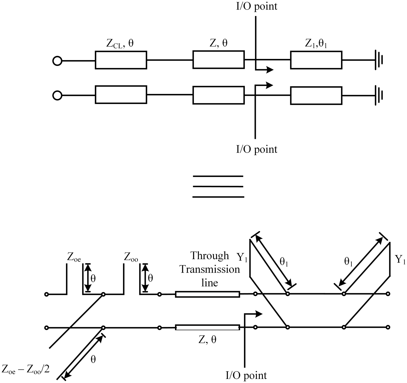
Figure 5 shows the third passband filter, which is designed using a modified coupling structure. The circuit comprises a novel MSICL resonator. Unlike standard designs, this MSICL structure incorporates asymmetric open- and short-circuited stubs within the coupling mechanism. This innovation allows for the independent control of transmission zeros and poles, which is critical for suppressing interference from the lower bands. Consequently, this hybrid configuration enables the direct integration of all three filters at a common junction without the need for external matching networks. The two open circuit stubs are connected in series with impedance 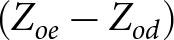 $(Z_{oe}-Z_{od})$/2. The through-coupled line in the center can be approximated by two unit elements with coupling between them. The input–output port is located at the junction between them. To the right of the circuit, there are two shunt short-circuited stubs with an admittance of Ye, which are separated by a series of short-circuited stubs with an admittance of
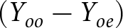 $(Y_{oo}-Y_{oe})$/2. The transfer matrix of the
 $BPF_3$ filter topology is shown in eq. 5. The filtering function can be calculated using the overall transfer matrix of the proposed circuit.
Schematic model of  $BPF_3$ with its equivalent circuit.

 \begin{align}
{T_{BPF3}} &= \prod\limits_{q = 1}^{2}\left[ \begin{array}{*{20}{c}}
{\cos ({\theta})}&{j{z_c}\sin ({\theta})} \nonumber\\
{\frac{{j\sin ({\theta})}}{{{z_c}}}}&{\cos ({\theta})}
\end{array} \right]
\times \prod\limits_{q = 1}^{2} {\left[ {\begin{array}{*{20}{c}}
1&{\frac{{- j{z_o}}}{{\tan (\theta )}}} \nonumber\\
0&1
\end{array}} \right]} \nonumber\\
&\quad \times \prod\limits_{q = 1}^{2}\left[ \begin{array}{*{20}{c}}
1&0\\ {\frac {-j}{z\tan
\left( \theta \right) }}&1\end{array} \right] \times
\left[ \begin {array}{cc} 1&0 \nonumber\\ {\frac {-j}{z\cot
\left( \theta \right) }}&1\end{array} \right]
\end{align}
The value of characteristic impedance for the  $BPF_3$ is a positive value, with the first couple line having an even-odd characteristic impedance of
 $Zo_{1} = 72.61$
 $\Omega$ and
 $Ze_{1} = 179.35$
 $\Omega$, and an electrical length of
 $\theta_{1} = 15^{o}$. The second couple line has a characteristic impedance of
 $Zo_{2} = 144.24$
 $\Omega$ and
 $Ze_{2} = 202.24$
 $\Omega$, with an electrical length of
 $\theta_{2} = 30^{o}$. The third couple line has the same characteristic impedance as the second couple line, and its electrical length is
 $\theta_{3} = 15^{o}$. The ideal frequency response of
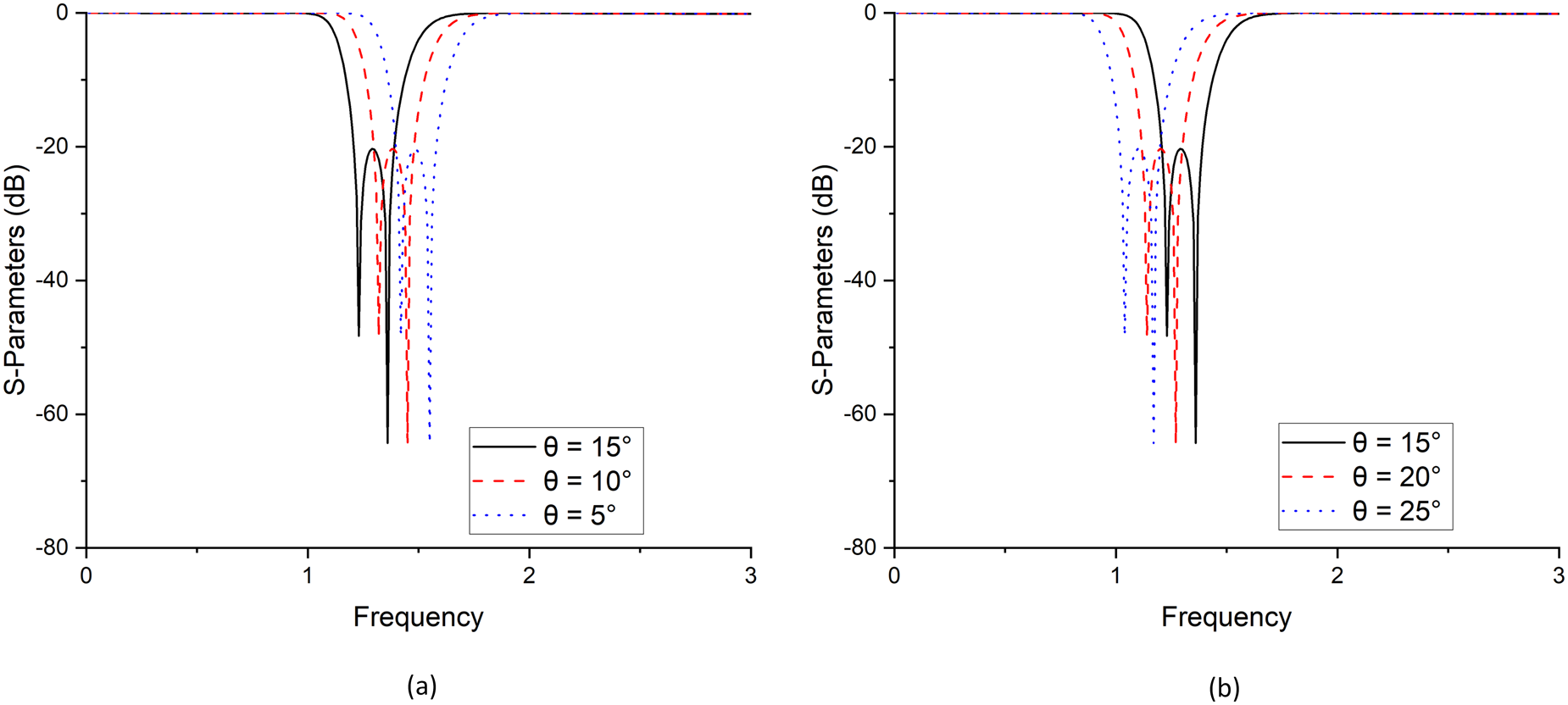
 $BPF_3$ is centered at 1.2 GHz, with 2 transmission poles, as illustrated in Figure 6. The resonant frequency of the filter can be adjusted by altering the electrical length. As illustrated in Figure 6(a) which shows that decreasing the electrical length will shift the resonant frequency to higher frequencies, and while Figure 6(b) depicts that increasing the electrical length will shift the resonant frequency to lower frequencies.
Frequency response of  $BPF_3$ with variable electrical length.

The passband filters  $BPF_1$,
 $BPF_2$, and
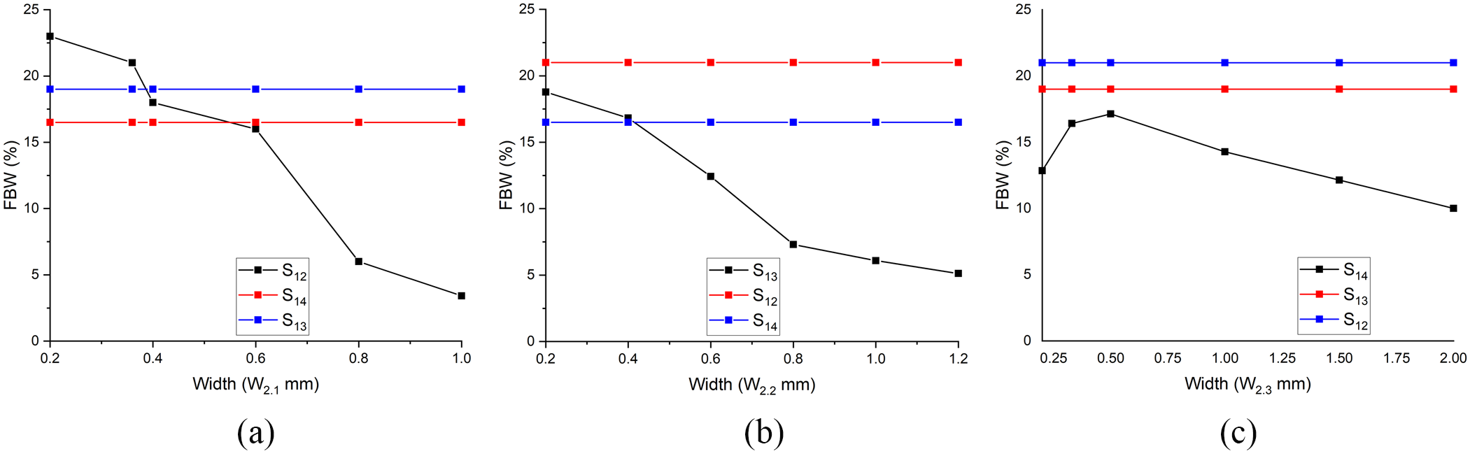
 $BPF_3$ are coupled in a way that ensures separation between all three filters to form a triplexer. Each filter can operate independently and keep its functionality according to this arrangement. The proposed triplexer model is shown in Figure 8. A detailed analysis reveals that, in addition to the effects of electrical length, the width of the coupled line also influences the FBW of all three passband filters. This phenomenon 5is illustrated in Figure 7. The FBW of the first passband decreases as the width of
 $W_2._1$ is reduced and increases as
 $W_3._1$ expands. However, as shown in Figure 7(a), the FBW of the second and third passbands remains unchanged. Conversely, as depicted in Figure 7(b), altering the width of
 $W_2._2$ in the coupled line affects the FBW of the second passband while leaving the FBW of the first and third passbands unaffected. Similarly, Figure 7(c) demonstrates that modifying the width
 $W_2._3$ leads to a shift in the FBW of the third passband while keeping the FBW of the first and second passbands constant. This behavior can be attributed to variations in the width of the coupled line, which directly impact its characteristic impedance, thereby influencing the FBW of the filter. These observations are critical for designing BPFs with precise frequency responses.
(a) Variation in FBW W.R.T  $W_2._1$, (b)Variation in FBW W.R.T
 $W_2._2$, and (c) Variation in FBW W.R.T
 $W_2._3$.

Result and measurements
Bandpass filter
As an ideal transmission line design is lossless, microstrip circuits inherently exhibit losses due to various contributing factors. These losses result in performance differences between the practical microstrip triplexer and its ideal counterpart. Therefore, optimizing microstrip-based designs is essential to minimize transmission losses and enhance overall circuit performance. When creating a microstrip design, the physical parameters are calculated from the electrical parameters of the ideal design. The basic structure of the triplexer is made of microstrip lines with tees and bends. Bends help in making the circuit more compact without compromising its electrical performance, while tees are used to connect or combine multiple resonators, stubs, and transmission lines. The physical parameters of the designed triplexer are calculated by a line calculator. The calculated dimensions are as follows:  $W_{in1}$ = 0.45 mm,
 $W_{in2}$ = 0.49 mm,
 $W_{in3}$ = 1.1 mm,
 $W_{in4}$ = 0.25 mm,
 $W_{1.1}$ = 0.50 mm,
 $W_{1.2}$ = 0.20 mm,
 $W_{1.3}$ = 4.5 mm,
 $W_{2.1}$ = 0.50 mm,
 $W_{2.2}$ = 0.20 mm,
 $W_{2.3}$ = 1.42 mm,
 $W_{3.2}$ = 0.20 mm,
 $W_{s1}$ = 0.90 mm,
 $L_{in1}$ = 14.96 mm,
 $L_{in2}$ = 7.90 mm,
 $L_{in3}$ = 6.62 mm,
 $L_{in4}$ = 5.0 mm,
 $L_{1.1}$ = 5.18 mm,
 $L_{1.2}$ = 5.80 mm,
 $L_{1.3}$ = 6.5 mm,
 $L_{2.1}$ = 13.45 mm,
 $L_{2.2}$ = 3.49 mm,
 $L_{2.3}$ = 11.0 mm,
 $L_{3.1}$ = 23.40 mm,
 $L_{3.2}$ = 20.0 mm,
 $L_{3.3}$ = 16.9 mm,
 $L_{s1}$ = 13.55 mm,
 $L_{s2}$ = 1.18 mm,
 $S_{1.1}$ = 0.24 mm,
 $S_{1.2}$ = 0.20 mm, and
 $S_{1.3}$ = 0.20 mm, respectively.
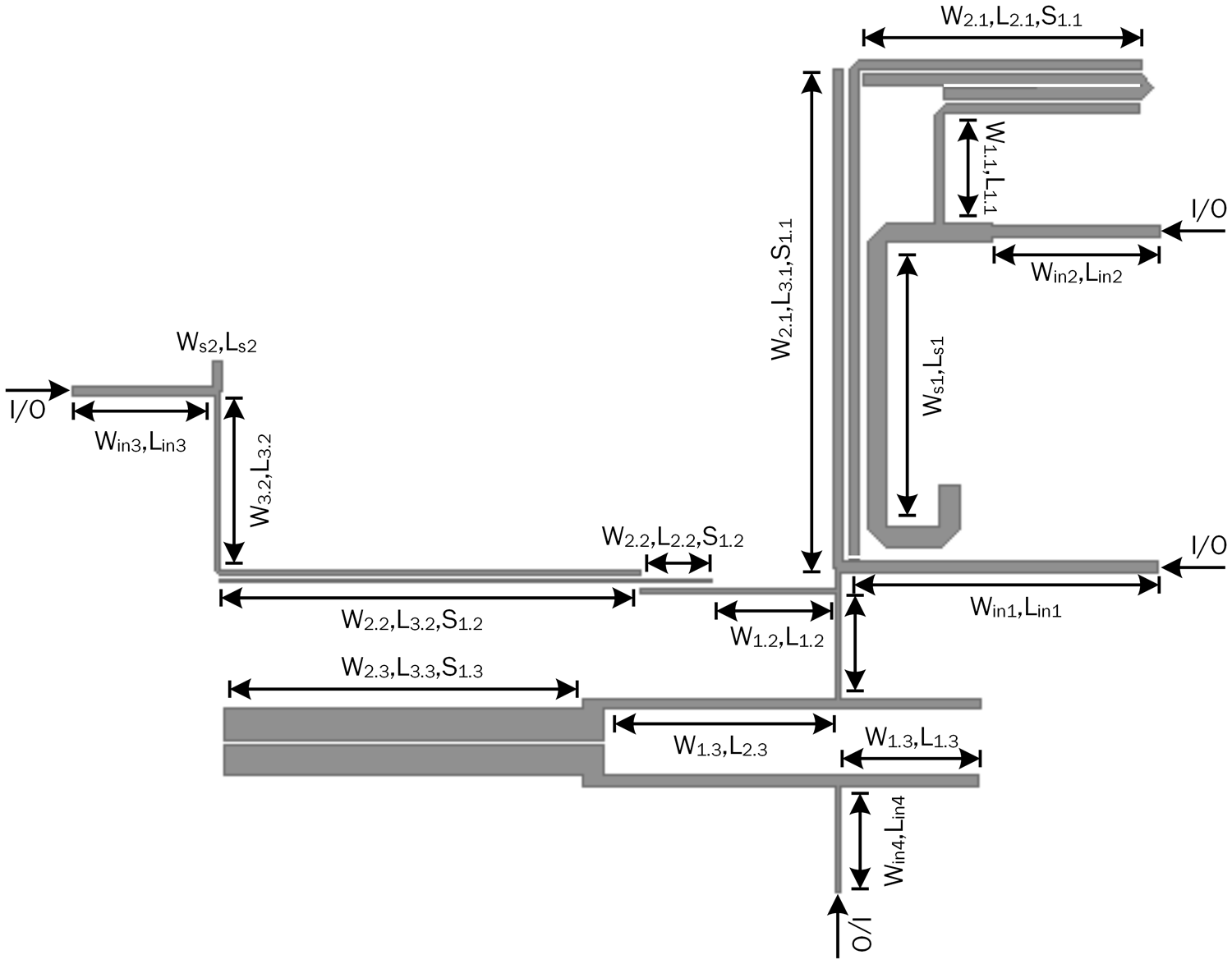
As shown in Figure 8,  $BPF_1$ is linked between port 1 and port 2, while
 $BPF_2$ is connected between port 1 and port 3 and
 $BPF_3$ is connected between port 1 and port 4. Port 1 is clearly designated as the input port, with ports 2, 3, and 4 acting as output ports. In the described setup, the proposed triplexer is designed by cascading all the BPFs. Figure 9 illustrates the S-parameter response of the proposed triplexer. We achieve three passbands centered at 2.91, 4.43, and 1.20 GHz, with FBWs of
 $30.2\%$,
 $22\%$, and
 $33.3\%$, respectively. Across all these passbands, the measured in-band return loss is better than 12.3 dB. Additionally, the proposed triplexer demonstrates three transmission poles for each of the first two passbands, while for
 $BPF_3$, we achieve two passbands.
Layout model of proposed Triplexer.

S-parameter response of the proposed triplexer.

Moreover, the in-band insertion loss for all three passbands is less than 0.63 dB. A slight frequency shift was observed between the individual filter design targets (2.88 and 4.0 GHz) and the final measured results of the triplexer (2.91 and 4.43 GHz). The observed frequency shift from 4.0 to 4.43 GHz is attributed to two factors: (1) Fabrication tolerances resulting in slight variations in the gap spacing ( $S_{1.2}$) of the coupled lines, which significantly alter the effective capacitance and (2) unaccounted parasitic coupling at the junction where the three filters merge. EM simulation, including the SMA connector models, confirms that the junction discontinuity contributes to this upward frequency shift. To validate the proposed topology against the theoretical model, a prototype was fabricated on a high-frequency substrate, specifically the Rogers Duroid 5880 substrate, with parameters (
 $\epsilon_r = 2.2$, tan
 $\delta = 0.0009$, and height
 $h = 0.787$ mm). The proposed triplexer was measured using an Agilent N5242A PNA-X.
To assess the practical robustness of the design, the impact of manufacturing tolerances was considered. In coupled-line structures, the coupling coefficient and consequently the bandwidth are highly sensitive to the gap spacing ( $S$). Standard chemical etching processes can introduce tolerances of
 $\pm 20$
 $\mu$m. Simulations show that reducing the gap by
 $10$
 $\mu$ (because of under-etching) increases the coupling, which makes the bandwidth wider and slightly lowers the center frequency. On the other hand, over-etching increases the gap, weakens the coupling, and shifts the frequency to a higher value. Additionally, variations in the substrate dielectric constant (
 $\epsilon_r$) directly affect the guided wavelength (
 $\lambda_g$). The observed shift in the third passband (from 4.0 to 4.43 GHz) suggests a combination of slight over-etching of the critical gaps in the MSICL resonator and minor variations in the substrate properties. Figure 10 shows the fabricated prototype of the proposed four-port triplexer.
Fabricated prototype of proposed triplexer.

Table 1 provides a detailed comparison between the proposed triplexer and the referenced papers. The proposed triplexer filter stands out for its remarkable features, such as improved selectivity, minimal insertion loss, and wider FBW, especially at higher frequencies. These advancements underscore the promising performance of the proposed design when compared to existing literature.
Comparison with recent proposed work

Conclusion
This paper presents a concise and efficient approach for designing a microstrip triplexer based on coupled-line structures integrated with open- and short-circuited stub resonators. The proposed triplexer comprises three interconnected BPFs linked through a junction network. Each BPF is specifically designed to operate at distinct frequency bands of 1.20, 2.91, and 4.43 GHz. By carefully optimizing the characteristic impedances, electrical length ratios, and coupling spacings between the resonators, the triplexer achieves excellent passband performance. The measured results indicate insertion losses of 0.6 dB at 1.20 GHz, 0.4 dB at 2.91 GHz, and 0.4 dB at 4.43 GHz. Additionally, the return loss remains better than 22 dB across all operating frequencies. Furthermore, the triplexer demonstrates FBWs of  $33\%$ at 1.20 GHz,
 $30\%$ at 2.91 GHz, and
 $22\%$ at 4.43 GHz. A comparative analysis is also provided, highlighting the superior passband characteristics of the proposed design relative to previously reported triplexer configurations.
Competing interests
The authors report no conflict of interest.
Appendix A: Summary of synthesis process
The triplexer is designed following a systematic eight-step synthesis process; the complete details from specification definition to final EM simulation are elaborated below:
(i) Set the center frequency, bandwidth, and selectivity requirements (including transmission zeros if needed) for each of the three channel filters.
(ii) Design a distributed equivalent structure for each channel filter based on ideal microstrip elements (transmission lines, stubs, coupled lines).
(iii) Identify and compute the transfer matrix (ABCD matrix) for each constituent component within the channel filters, including transmission lines, short-circuit stubs, open-circuit stubs, and coupled line sections.
(iv) Calculate the overall transfer matrix for each channel filter by cascading individual component matrices. Subsequently, generate the characteristic polynomials for each individual channel filter from these matrices.
(v) Verify both the mathematical synthesis (polynomials/matrices) and the microstrip model responses for each channel to ensure they are well-matched, confirming zero error in the synthesis process before proceeding.
(vi) Integrate all three channel filters with the appropriate combining structure (e.g., star-junction or manifold) to form a four-port triplexer (one common port and three channel ports) for analyzing mutual loading effects between channels.
(vii) Implement the physical combining structure, assemble the complete triplexer, and conduct full electromagnetic (EM) simulation verification. Fine-tune dimensions as necessary to meet specifications.
(viii) Once the filter response is fully optimized and validated through EM simulation, proceed with fabrication and physical implementation.
Appendix B: Filtering coefficient
Here, 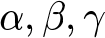 $\alpha, \beta, \gamma$, and
 $\zeta$ are complex filtering coefficients. The filtering coefficient equations are a function of the characteristic impedance of the design topology.
 \begin{align}
\alpha &=1/4\, \left( 2\,Z+\textit{Ze}+\textit{Zo} \right) \left( 6\,{\textit{Ze}}^{3}z+10\,{\textit{Ze}}^{2}z\textit{Zo}+10\,{\textit{Zo}}^{2}\textit{Ze}\,Z+6\,{\textit{Zo}}^{3}Z\right. \nonumber\\ &\quad \left.+3\,{\textit{Ze}}^{4}+4\,{\textit{Ze}}^{3}\textit{Zo}+2\,{\textit{Ze}}^{2}{\textit{Zo}}^{2} +4\,{\textit{Zo}}^{3}\textit{Ze} +3\,{\textit{Zo}}^{4}-
24\,\textit{Ze}\,Z-24\,Z\textit{Zo}\right. \nonumber\\ &\quad \left.-12\,{\textit{Ze}}^{2}-8\,\textit{Ze}\,\textit{Zo}-12\,{\textit{Zo}}^{2}\right) \left( \textit{Ze}+
\textit{Zo} \right) \left( {Z}^{2}-1
\right) ((Ze-Zo)^4 \ast Z^2)^{-1}
\end{align}
 \begin{align}
\beta &= 1/16\, \big( 13\,{A}^{2}-12 \big) {\textit{Ze}}^{6}+1/16\, ( 52\,
{Z}^{3}+14\,{Z}^{2}\textit{Zo}-52\,Z\,8\,\textit{Zo} {\textit{Ze}}^{5} \nonumber\\
&\quad +1
/16\, \big( \big( 3\,{Z}^{2}+12 \big) {\textit{Zo}}^{2}+ ( 52\,
{Z}^{3}
-52\,Z ) \textit{Zo}+ 52\,{Z}^{4}-112\,{Z}^{2}+52\big) {\textit{Ze}}^{4}\nonumber\\
&\quad+1/16\, ( ( 4\,{Z}^{2}+16 ){\textit{Zo}}^{3} +( 24\,{Z}^{3}-24\,Z) {\textit{Zo}}^{2}+ ( 48\,{Z}^{4}-
128\,{Z}^{2} + 48)\nonumber\\
&\quad\times \textit{Zo}-208\,{Z}^{3}+208\,Z) {\textit{Ze
}}^{3} +
1/16\, ( ( 3\,{Z}^{2}+12) {\textit{Zo}}^{4} \!+\!( 24\,{Z}^{3}-24\,Z) {\textit{Zo}}^{3}\nonumber\\
&\quad + ( 56\,{Z}^{4}-
160\,{Z}^{2}+56) {\textit{Zo}}^{2} +( -304\,{Z}^{3}+304\,Z) \textit{Zo}-192\,{Z}^{4}\nonumber\\
&\quad +
208\,{Z}^{2} ) {\textit{Ze}}^{2}+3 \,( ( {\frac {7\,{Z}^{2}}{12}}-1/3 ) {\textit{Zo}}^{3}+( {Z}^{3}-3/2\,Z )\nonumber\\ & \quad \times {\textit{Zo}}^{2}+ ( -7/3\,{Z}^{2}+
2) \textit{Zo}-8\,{Z}^{3}+{\frac {26\,Z}{3}} ) \textit{Zo}\,(Z+\textit{Zo}/2) \textit{Ze} \nonumber\\
&\quad +\frac {13\,{\textit{Zo}}^{2}
(Z+\textit{Zo}/2) ^{2}}{4} ( ( -{\frac {12}{13}}
+{Z}^{2}) {\textit{Zo}}^{2}-{\frac {4\,z\textit{Zo}}{13}} \nonumber\\
&\quad -{\frac {48
\,{Z}^{2}}{13}}+4 ) \textit{Zo} ) ( {Z}^{2}-1
) ((Ze-Zo)^4 \ast Z^2)^{-1}
\end{align}
 \begin{align}
\gamma &=1/8\, ( -3\,{Z}^{2}+2) {{Ze}}^{6}+1/8\,( -12\,{Z
}^{3}+2\,{Z}^{2}{Zo}
+12\,Z-4\,{Zo}) {{Ze}}^{5} \nonumber\\
&\quad +1/8
\, (( 3\,{Z}^{2}-2) {{Zo}}^{2}+( 12\,{Z}^
{3}-
12\,) {Zo}-12\,{Z}^{4}+32\,{Z}^{2}-12) {{Ze}}^{4}\nonumber\\
&\quad+1/8 ( -4\,{Z}^{2}+
8) {{Zo}}^{3}+( 16\,{Z}^{4}-16\,{Z}^{2}+16) {Zo}+48\,{Z}^{3}-48\,Z) {{Ze}}^{3}\nonumber\\
&\quad
+1/8\, ( ( 3\,{Z}^{2}-2 ) {{Zo}}^{4}+ ( -8\,{Z}^{4}+32\,{Z}^{2}-8) {{Zo}}^{2}
+( 16\,{Z}^{3}-16\,Z) {Zo}\nonumber\\
&\quad+32\,{Z}^{4}-48\,{Z}^{2}) {{Ze}}^{2}+ 2\,{Zo}\,(Z
+{Zo}/2)(( -1/2+1/4\,{Z}^{2} ) {{Zo}}^{3}\nonumber\\
&\quad+({Z}^{
3}-Z/2) {{Zo}}^{2}\!+\!
(-{Z}^{2}+2) {Zo}+4\,{
Z}^{3}-6\,Z) {Ze}-3/2\,{{Zo}}^{2} (Z+{Zo}/2) ^{2}\nonumber\\
&\quad \times
((-2/3+{Z}^{2}) {{Zo}}^{2}-4/3\,
Z{Zo}-8/3\,{Z}^{2}+4)
\times((Ze-Zo)^4 \ast Z^2)^{-1}
\end{align}
 \begin{align}
\zeta &=1/16\, ( 2\,{\textit{Ze}}^{2}{Z}^{2}-4\,\textit{Zo}\,\textit{Ze}\,{Z}^{2}+
2\,{\textit{Zo}}^{2}{Z}^{2}+{\textit{Ze}}^{3}Z
-{\textit{Ze}}^{2}Z\textit{Zo}-{{Zo}}^{2}\textit{Ze}\,Z\nonumber\\
&\quad +{\textit{Zo}}^{3}Z-4\,\textit{Ze}\,Z-4\,Z\textit{Zo} -2\,{\textit{Ze}}^{2}+4
\,\textit{Ze}\,\textit{Zo}-2\,{\textit{Zo}}^{22} \nonumber\\
&\quad \times ((Ze-Zo)^{4} \ast Z^{2})^{-1}
\end{align}

Muhammad Abdul Rehman received his Bachelor’s and M.Sc. degrees in Computer Sciences and Telecom Systems from Bahauddin Zakariya University, Multan, Pakistan. He later earned his M.S. and Ph.D in Electrical Engineering from Riphah International University, Islamabad, Pakistan. Currently, he is serving as an Assistant Professor at Superior University Lahore. His current research interests include RF and microwave passive devices, microstrip components, and related electromagnetic structures.

Bilal Mushtaq obtained his Bachelor of Science and Master of Science degrees in Electrical Engineering from HITEC University in Taxila, Pakistan. He served as a Lecturer in the Electrical Engineering Department at Foundation University Rawalpindi Campus in Rawalpindi, Pakistan, for 8.5 years and 3 years in the Electrical and Computer Science Department of Riphah International University, Islamabad, Pakistan. He earned his Ph.D. in Electrical Engineering from Riphah International University, Islamabad, Pakistan. Currently, he is working as an Assistant Professor in Electrical and Electronic Engineering Department at Beaconhouse International College, Islamabad, Pakistan. His research interests encompass various areas, including the development and integration of microwave filters, secure communication techniques, machine learning, artificial intelligence, and sustainable energy solutions.