Introduction
Impetus for new technologies for renewable energy has escalated with increasing global energy demand. From clean and renewable view point, hydrogen has attracted significant interest as a promising method for energy storage since it does not contribute to the greenhouse effect when it is produced in clean and renewable way. Although there are technical approaches to produce hydrogen by electrolysis[ Reference Millet, Grigoriev and Diéguez 1 ] or thermolysis,[ Reference Baykara 2 ] the energy required for H2 production generally results from fossil fuel or coal-based sources.[ Reference Armaroli and Balzani 3 ] In this context, hydrogen production from photoelectrochemical (PEC) water splitting using earth abundant material and solar energy is of significant interest. Photoactive materials with band gap energies corresponding to water-splitting potential have been widely tested as photoelectrodes to facilitate the solar light harvesting.[ Reference Maeda and Domen 4 ] Among the potential photoanode materials, hematite (α-Fe2O3) is a promising option due to its chemical stability, abundance, and adequate band gap[ Reference Cesar, Sivula, Kay, Zboril and Grätzel 5 – Reference Mohapatra, John, Banerjee and Misra 7 ] that predictably offers a maximum photocurrent density and photoconversion efficiency of 12.6 mA/cm2 and 12.9%, respectively.[ Reference Sivula, Le Formal and Grätzel 8 , Reference Murphy, Barnes, Randeniya, Plumb, Grey, Horne and Glasscock 9 ] However, the practically obtained values for photocurrent are far less than the theoretical ones due to short hole diffusion length (2 × 10⁻⁶ cm) and fast charge carrier recombination in hematite, which limit its PEC performance.[ Reference Dare-Edwards, Goodenough, Hamnett and Trevellick 10 ] Moreover, an inadequate conduction band position poses thermodynamic barriers on the photogenerated electrons, so that an external bias is required to transfer them to external circuit. To improve the PEC performance of Fe2O3 several experimental strategies have been demonstrated such as elemental doping to enhance mobility of charge carriers,[ Reference Kleiman-Shwarsctein, Hu, Forman, Stucky and McFarland 11 – Reference Ling, Wang, Wheeler, Zhang and Li 13 ] controlling surface properties of nanostructured photoanodes,[ Reference Warren, Voïtchovsky, Dotan, Leroy, Cornuz, Stellacci, Hébert, Rothschild and Grätzel 14 ] and fabrication of heterojunction layers.[ Reference Yang, Liu, Du, Dai, Zheng and Wang 15 , Reference Liu, Zheng, Spurgeon and Yang 16 ] Fabrication of heterojunction is thought to be a promising approach for designing efficient thin-film photoanodes since judiciously chosen semiconductor bi-layers can shift the absorption maximum toward visible range and a favorable band alignment can additionally enhance charge separation in heterojunction materials.
A large body of data exists on the fabrication of heterojunction photoanodes based on Fe2O3 films designed to enhance the PEC performance. Iron oxide is also a compatible host for electronic modification both in bulk (doping) and thin-film (interfaces) forms, for instance, by incorporation of Ti(IV) centers in iron oxide lattice or by forming Fe2O3//TiO2 nanolaminates. Given several intrinsic advantages, such as strong photoactivity, chemical stability, TiO2-based photoanodes for PEC water oxidation have been widely investigated.[ Reference Fujishima and Honda 17 ] Intimate mixing of Fe2O3 and TiO2 nanolayers carry the potential of integrating higher absorption cross-section of iron oxide with the high-charge carrier mobility in titanium oxides. For instance, Kim et al.[ Reference Kim, Oh, Yun, Jung, Kang and Kim 18 ] reported enhanced PEC performance in Fe2O3/TiO2/FTO composite layers demonstrated by drastic improvement of photocurrent density under UV/visible illumination, when compared with pristine Fe2O3/FTO films. They proposed that morphology of TiO2 nanotubes facilitates electron transfer thereby reducing electron–hole recombination in the composite structure. This study shows that there was an optimum amount α-Fe2O3 covering the TiO2 layer to enhance PEC performance of heterojunction photoanode. As our group recently reported,[ Reference Wang, Pyeon, Gonullu, Kaouk, Shen, Guo and Mathur 19 , Reference Mettenbörger, Gönüllü, Fischer, Heisig, Sasinska, Maccato, Carraro, Sada, Barreca, Mayrhofer, Moseler, Held and Mathur 20 ] PEC performance of hematite-based photoanodes can be enhanced not only due to Sn diffusion (from FTO or ITO substrates) triggered by post-annealing necessary for obtaining crystalline films, which results in composite Fe2O3/TiO2 photoelectrodes with multiple interfaces and heterojunctions. In this study, we fabricated multilayers consisting of Fe2O3 and TiO2 to investigate the effect of not only the multilayers, but also that of multiple heterojunctions in the determination of the limiting factor for charge separation, orthogonality of heterojunctions, and its influence on charge carrier transport as a function of film thickness and structural patterns. The role of multiple phase boundaries in Fe2O3–TiO2 heteroarchitectures in influencing water oxidation reactions can provide better insight in the design of composite electrodes based on multi-material compositions. Interface modulation by sequential PECVD of Ti and Fe precursors allowed us to grow Fe2O3//TiO2//Fe2O3:FTO multi-junction structures with striped and cross-bar patterns. Besides increasing the numerical density of the active sites, the fabricated three-dimensional (3D) cross-bar structures could potentially decouple the heterojunctions from the substrate influence to elucidate the importance of space-charge region in the separation of photocarriers.
Experimental
Preparation of TiO2 and Fe2O3 layers
Photoanode materials were fabricated by a radio frequency (13.56 MHz) plasma enhanced chemical vapor deposition (PECVD) on fluorine-doped tin oxide glasses (FTO, ~13 Ω/sq, Sigma Aldrich). FTO substrates were cleaned with deionized water and isopropyl alcohol by placing them for 10 min in an ultrasound sonication bath followed by plasma treatment with argon to eliminate surface adsorbed molecules. Iron pentacarbonyl [Fe(CO)5, Acros Organics] and titanium tetraisopropoxide (C12H28O4Ti, Acros Organics) used as precursors of Fe2O3 and TiO2, respectively, were employed without further purification. Oxygen gas was introduced into the PECVD chamber as source of oxidizing gas. The precursor flow rate was controlled by monitoring pressure in the chamber. The operating condition with plasma power of 100 W was maintained as already optimized in our previous study.[ Reference Mettenbörger, Singh, Singh, Järvi, Moseler, Valldor and Mathur 21 ] The multi-layered samples were annealed at 550 °C for 5 h and at 750 °C for 2 h to obtain crystalline phases of TiO2 and Fe2O3, respectively, in ambient condition. Especially for TiO2 layer deposition, the deposition time varied to investigate the effect of the thickness on PEC performance. The annealing process was carried out after each deposition had been accomplished with the parameters above for the multi-layered structure.
Construction of patterned composite film
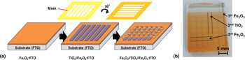
Metallic masks featuring 17 mm × 2 mm of holes and 1 mm of space among them were employed to fabricate patterned Fe2O3 and TiO2 electrodes [see Fig. 1(a)]. The first layer was deposited on FTO substrate without putting a mask to ensure continuous contact between the substrate and the basal layer, while the second and third layers were deposited with the mask put on the first-deposited layer to build cross-bar structures. Especially, the third layer was deposited in the manner of 90° rotated to the second layer, so single, double, and triple layers were simultaneously fabricated on a FTO substrate [Fig. 1(b)]. The sample was annealed after each layer was deposited.
(a) A schematic procedure of fabricating the Fe2O3//TiO2//Fe2O3:FTO patterned multilayer and (b) the photograph of prepared sample of Fe2O3//TiO2//Fe2O3:FTO.

Morphological and structural characterization
The surface morphologies of deposited layers were observed by a scanning electron microscope (SEM, Lyra 3-FEG, TESCAN) and estimated roughness was determined by an atomic force microscope (AFM, XE-100, Park Systems). Moreover, the energy-dispersive x-ray spectroscopy (EDX, Lyra 3-GMU, TESCAN) mapping has been conducted to observe elemental distribution of each area on the patterned surface. Qualitative surface analyses of the samples were investigated by x-ray photoelectron spectroscopy (XPS, M-Probe monochromatic, Surface Science Instruments). Micro-Raman spectroscopy (514 nm Ar laser, Rienshaw) was carried out to study vibrational modes of fabricated films on specific areas. An x-ray diffraction (XRD) pattern was obtained from STOE-STADI MP diffractometer using Cu Kα radiation and calculation of a diffraction pattern was conducted by Materials Analysis Using Diffraction.
PEC measurement of the photoanodes
Photocurrent density versus saturated calomel electrode (SCE) was measured with a three-electrode PEC cell using a potentiostat (Versastat, USA) and a 150 W Xenon lamp (Oriel, AM 1.5 G filter). The scan range and rate of potential (V/SCE) were from −1 to 1 and 10 mV/s, respectively. The dark current and current under simulated solar light were measured in 1 M NaOH solution. The J–V data shown in this paper are converted into V/RHE scale using the following equation, E RHE = E SCE + E o SCE + 0.059 pH.
Results and discussion
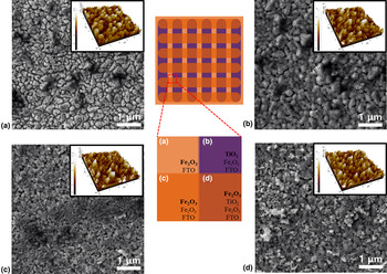
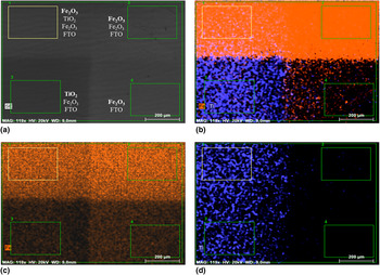
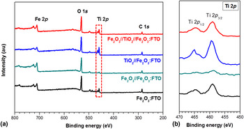
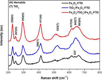
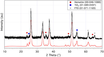
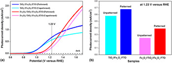
To investigate the effects of multi-junctions on PEC performance of Fe2O3–TiO2 photoanodes, initial layer Fe2O3 was fully covered on FTO and used to construct different junctions (Fe2O3//TiO2//Fe2O3:FTO) on Fe2O3 layer, as shown in Fig. 1(b). The cross-bar structure of the obtained photoanode showed well-defined boundaries without having any blurred lines that would imply uncontrolled intermixing. To elucidate the influence of patterning fully covered, unpatterned, bilayer and triple layers were also fabricated and investigated toward their PEC properties. AFM and SEM measurements (Fig. 2) showed homogeneous surface with granular morphology. However, denser surfaces with small aggregated particles were observed on Fe2O3//Fe2O3:FTO [Fig. 2(c)] and Fe2O3//TiO2//Fe2O3:FTO areas [Figs. 2(b)–2(d)]. AFM topologies and surface roughness values of different areas on patterned Fe2O3//TiO2//Fe2O3:FTO are shown (Fig. 2 and Table I), which indicated that the cross-bar structured photoanodes have an active surface with various morphologies. The EDX mapping was conducted to investigate elemental distribution in the patterned Fe2O3//TiO2//Fe2O3:FTO structure, as shown in Fig. 3. The boundaries of differential element concentrations could be clearly observed, confirming the successful construction of patterned structures, as shown in the schematic plots in Fig. 2. Due to annealing at high temperature (750 °C), in-plane atomistic diffusion of either Ti to Fe2O3 or Fe to TiO2 cannot be ruled out, which can facilitate the PEC performance as reported previously.[ Reference Fu, Jiang, Liu, Wang, Wang and Xie 22 – Reference Khan, Woo and Yang 26 ] XPS analysis provided the elemental composition on the surface of the patterned triple layer (Fig. 4). Fe 2p at ~711.0 eV and Ti 2p at ~459 eV peaks observed commonly in all area of the triple layer of the patterned sample support lateral and/or vertical inter-atomic diffusion. Especially, the Ti 2p peaks observed on Fe2O3//TiO2//Fe2O3:FTO area clearly indicate that there could be diffusion of Ti species either from the neighboring TiO2//Fe2O3:FTO region or from its TiO2 underlayer during the process. Moreover, chemical shifts in Ti 2p 3/2 peaks on each area can be explained by the fact that atomic environment of Ti in the crystal structure of Fe2O3 is different from that in TiO2.[ Reference Deng, Zhong, Pu, Zhang, Li, Sun and Lee 27 ] In Fig. 5, Raman spectra of patterned Fe2O3//TiO2//Fe2O3:FTO samples showed vibrational modes at 226, 247, 293, and 411 cm−1 corresponding to hematite phase.[ Reference de Faria, Venâncio Silva and de Oliveira 28 ] Typical TiO2 peaks including B1 (396 cm−1), B1g (523 cm−1) and A1g (642 cm−1) correspond to vibrational modes of anatase TiO2 on the TiO2//Fe2O3:FTO area (blue).[ Reference Pena-Flores, Palomec-Garfias, Marquez-Beltran, Sanchez-Mora, Gomez-Barojas and Perez-Rodriguez 29 ] In addition, a small peak at 637 cm−1 is observed in the Fe2O3:FTO area (black), which can be assigned to A1g vibrational mode of SnO2.[ Reference Katiyar, Dawson, Hargreave and Wilkinson 30 ] The 663 cm−1 peak from Fe2O3 is often the case of hematite, which is related to disorder effects and/or to the presence of nanocrystals.[ Reference Bersani, Lottici and Montenero 31 ] Moreover, coexistence of hematite and anatase TiO2 was confirmed by using XRD from the patterned Fe2O3//TiO2//Fe2O3:FTO sample (Fig. 6). Apart from the prominent SnO2 (PDF 41-1445) peaks, hematite (PDF 33-0664) peaks (012), (110), (024), and (300) are observed at 24.1°, 35.6°, 49.4°, and 63.9°, respectively. Although it is challenging to distinguish the crystalline phase of TiO2 due to comparably intense signals from either SnO2 or hematite, the shoulder at 25.3° can be assigned to anatase TiO2 (PDF 21-1272) that apparently emerges from small TiO2 area exposed on the surface of the cross-bar structure. J–V curves (Fig. 7), obtained by a three-electrode measurement mentioned, showed that onset potential of the triple layer samples presents an anodic shift for both patterned and unpatterned photoanodes [Fig. 7(a)], leading to suppressed photocurrent density at lower potential range. This anodic onset shift is also observed when the multi-layered samples are compared with the single layer of Fe2O3. Thus, the deposition of second layer of TiO2 decreased the PEC performance at lower potential (Fig. S1), which could be attributed to the mismatch of the band structures between Fe2O3 and TiO2 (Scheme 1).[ Reference Kudo and Miseki 32 ] Interestingly, when the third Fe2O3 layer was deposited, quite different photocurrent curves were observed for both unpatterned and patterned samples. Compared with single-layered Fe2O3 and double-layered TiO2//Fe2O3:FTO, the photocurrent densities of triple-layered samples displayed decreased photocurrent densities at lower applied potential, but after a certain potential a rapid increase was observed. At an applied potential of 1.7 V versus RHE, Fe2O3//TiO2//Fe2O3:FTO samples showed photocurrent densities of 1.87 and 2.01 mA/cm2 for unpatterned and patterned structures, respectively, which are significantly higher than that of Fe2O3 single layer (1.39 mA/cm2). However, it cannot be concluded that the triple-layered samples are more efficient photoanodes than the single layer of Fe2O3 for PEC water splitting because the current density obtained at high applied potential range is not regarded as a result of PEC reaction of the material but rather it comes from electrochemical reaction due to high-energy input. Nevertheless, it is noteworthy that the patterned double and triple photoanodes demonstrated better PEC performance than the unpatterned multilayers in the whole range of the applied potential [Fig. 7(a)]. In addition, the thickness effect of TiO2 used as an electron transfer material[ Reference van Hal, Wienk, Kroon, Verhees, Slooff, van Gennip, Jonkheijm and Janssen 33 , Reference Bach, Lupo, Comte, Moser, Weissortel, Salbeck, Spreitzer and Gratzel 34 ] was investigated to elaborate J–V characteristics as a function of deposition time of TiO2 (Fig. S2). As deposition time of TiO2 increases, which implied thicker titania layers the photocurrent density was found to decrease even at higher potential. This indicates the photogenerated electrons are not driven to external circuit to generate current, so photocurrent density generated through whole device structure is lower than that of single layer of Fe2O3. We assume that photogenerated electrons at the top layer of Fe2O3 can be transported to TiO2 interlayer due to high over potential in spite of inappropriate band alignment between Fe2O3 and TiO2. Especially when the TiO2 interlayer is thinner, electrons transported from the Fe2O3 at higher potential have low probability to recombine with holes in bulk comparing with thicker TiO2 interlayer (Scheme 1). The PEC performances of composite electrodes suggest that: (1) the patterned structure created heterojunctions not only along the vertical axis of FTO substrate, but also along the horizontal axis, providing new transfer routes for photogenerated electron and hole pairs; (2) the patterned structure augments specific surface areas between photoanodes and electrolyte; (3) the cross-bar structures promoted lateral and/or vertical elemental diffusion to create compositional gradients in films that are beneficial for charge carrier transport (Fig. 3). To construct multiple junctions and heterofunctional interfaces to obtain photoelectrodes with improved contact and transport properties, new strategies in conjunction with PECVD process such as spray pyrolysis,[ Reference Chiang, Aroh, Franson, Satsangi, Dass and Ehrman 35 – Reference Mariño-Otero, Oliver-Tolentino, Aguilar-Frutis, Contreras-Martínez, Pérez-Cappe and Reguera 37 ] pulsed laser deposition,[ Reference Cao, Liu, Hashimoto and Ye 38 , Reference Lee, Park, Han, Song, Cho, Noh and Hong 39 ] and high-throughput “parallel” material growth method[ Reference Mao 40 ] are potentially interesting. Moreover, enhanced photoactivity even at lower applied potential can be achieved by surface-functionalization strategies (e.g., Co–Pi catalyst) of 3D heterostructure to shift onset potential in cathodic direction.[ Reference Lee, Shinde, Go and Doh 41 ]
Surface morphologies and topologies (insets) of each area resulted from patterning of a Fe2O3//TiO2//Fe2O3:FTO triple layer (center: a scheme of the patterned triple layer).

EDX elements mapping on the Fe2O3//TiO2//Fe2O3:FTO sample: (a) microscopic image of the patterned sample, (b) combined elemental mapping image of Fe and Ti, (c) selective Fe mapping image, and (d) selective Ti mapping image; Fe2O3//TiO2//Fe2O3:FTO for square 1, Fe2O3//Fe2O3:FTO for square 2, TiO2//Fe2O3:FTO for square 3, and Fe2O3:FTO for square.

(a) XPS spectra of each area and (b) enlarged spectra of Ti 2p peaks on the patterned triple layer.

Raman spectra of different areas; (black) Fe2O3:FTO, (blue) TiO2//Fe2O3:FTO, and (red) Fe2O3//TiO2//Fe2O3:FTO on the patterned triple layer.

(Solid black line) X-ray diffraction pattern of the patterned Fe2O3//TiO2//Fe2O3:FTO and (dotted red line) refined pattern.

PEC performance of unpatterned and patterned samples; (a) linear scan voltammetry measured in 1 M NaOH under illumination with 150 W Xe lamp (AM 1.5 G filter) (b) photocurrent density values at 1.23 V versus RHE.

Surface roughness values (root-mean-square) of selected surface areas in the patterned photoanode.

Conclusions
In this work, simple and patterned Fe2O3//TiO2//Fe2O3:FTO architectures were fabricated to understand the role of multiple heterojunctions in multi-layered systems and their effect on transport and dynamics of photogenerated charge carriers. The concentration gradient created in lateral and vertical mixed-oxide (Fe2O3 and TiO2) structures offers a simplistic way of modulating the local electronic properties of heterojunctions. It was observed that the multiple junctions and interfaces between Fe2O3 and TiO2 derived by macro-patterning enhanced the specific surface and interfacial areas; however, the orthogonality of band gap energies can create electronic blockades as reflected in the poor PEC efficiency of some of the composite electrodes. In terms of PEC performances of the prepared samples anodic onset shifts were observed from both unpatterned and patterned multilayers, which are undesirable, due to increased number of recombination sites, interfaces, and band alignment. Nevertheless, enhanced photocurrent density values at 1.23 V versus RHE were obtained from the patterned double layer (0.68 mA/cm2) and the triple layer (0.39 mA/cm2), whereas those of the unpatterned double and triple samples exhibited 0.58 and 0.25 mA/cm2, respectively. Although the photocurrent density of patterned triple layer obtained at water redox potential (1.23 V versus RHE) is lower than that of the single layer of Fe2O3 due to increased recombination sites (e.g., expected transient phase of Fe2O3 and TiO2), still, it is noteworthy that there is an effect of macro-patterning, when we compare double and triple heterojunction photoelectrodes fabricated with and without using the mask. Besides, it was revealed that increasing thickness of intercalated TiO2 is detrimental for electron transport properties. In conclusion, fabricating multiple junctions is effective for enhancing PEC performance; however, elucidation of the phenomena occurring at the interfaces and surfaces require further efforts.
Supplementary material
The supplementary material for this article can be found at https://doi.org/10.1557/mrc.2016.54.
Acknowledgments
This work was financially supported by SOLAROGENIX, Project (EC-EP6-Grant Agreement No. 214281) and the University of Cologne, Germany.