Introduction
Nanoscale metal–metal multilayered materials can be considered a model system to design new interfaces as a possible structural metal. The enabling factor in these multilayered nanolaminates is the interface interaction between the two metals that enables these novel properties of ultrahigh strength, sinks for radiation-induced defects, obstacles to deflect and hinder crack growth, and thermal stability up to 800 °C. An example can be seen from the use of the Cu/Nb multilayered nanocomposite, a type of nanoscale metal–metal multilayered composite, as a potential radiation damage-tolerant material [Reference Misra, Demkowicz, Zhang and Hoagland1, Reference Zhang, Fu, Li, Misra, Wang, Shao and Wang2, Reference Beyerlein, Caro, Demkowicz, Mara, Misra and Uberuaga3].
Plasticity in nanoscale metal–metal multilayered materials has been observed experimentally. Metallic multilayered nanolaminates of soft metals such as copper, nickel, and niobium with the strength of a few tens of MPa in bulk can achieve the flow strength of more than 2–3 GPa experimentally through nanoindentation experiments [Reference Anwar Ali and Budiman4, Reference Misra5, Reference Misra, Verdier, Lu, Kung, Mitchell, Nastasi and Embury6]. The hardness of these nanolaminates scales inversely with the square root of the individual layer thickness, h, at larger layer thicknesses but tapers off at lower thicknesses [Reference Fu, Li, Misra, Hoagland, Wang and Zhang7, Reference Zhang, Wu, Zhang, Wang, Liu and Sun8]. Misra et al. [Reference Misra5, Reference Misra, Hirth and Hoagland9, Reference Misra and Hoagland10, Reference Misra, Verdier, Kung, Embury and Hirth11] developed dislocation models on nanoscale metal–metal multilayered materials to describe the relationship between multilayer flow strength and individual layer thickness. They are the dislocation pile-up model, the confined layer slip model (CLS), and the interface crossing model depending on the range of individual layer thickness. These concepts were initially confirmed by atomistic modeling of the multilayered interfaces [Reference Wang, Hoagland, Hirth and Misra12, Reference Wang13, Reference Wang, Hoagland and Misra14].
It was only through in situ transmission electron microscope (TEM) nanoindentation experiments that dislocation plasticity behavior in multilayered nanolaminates was observed in real time with the focus on interface structures, dislocation nucleation, dislocation climb, and interface shear resistance [Reference Li, Wang, Huang, Misra and Zhang15, Reference Li, Fang, Xia and Feng16, Reference Li, Wang, Misra and Huang17]. Further, in situ and ex situ micropillar compression experiments on nanoscale metal–metal multilayered materials confirmed the ultrahigh flow strength values with plasticity mechanisms of the onset of yield, work hardening, and shear banding which can be attributed to their interfaces [Reference Mara, Bhattacharyya, Dickerson, Hoagland and Misra18, Reference Mara, Bhattacharyya, Hirth, Dickerson and Misra19, Reference Mara and Beyerlein20].
Experimentally, Budiman et al. [Reference Budiman, Li, Wei, Baldwin, Xiong, Luo, Trugman, Jia, Tamura, Kunz, Chen and Misra21] grew nanoscale single crystal metal–metal multilayered materials and performed synchrotron X-ray microdiffraction (µSXRD) Laue and monochromatic scans on successive ex situ compressions (before and after) at 5 different strain points up to the accumulative strain of 35% [Reference Budiman, Han, Li, Wei, Dickerson, Tamura, Kunz and Misra22, Reference Budiman, Narayanan, Li, Wang, Tamura, Kunz and Misra23]. The µSXRD technique can characterize the microstructure, plasticity, and stress and its evolution in a particular micron/nanoscale location in many crystalline applications [Reference Anwar Ali, Kunz, Tamura and Budiman24, Reference Budiman25, Reference Budiman, Han, Greer, Tamura, Patel and Nix26, Reference Feng, Budiman, Nix, Tamura and Patel27, Reference Jiang, Wu, Su, Liu, Chia, Li, Son, Oh, Byun, Kim, Im, Huang and Ho28, Reference Liu, Thadesar, Taylor, Oh, Kunz, Tamura, Bakir and Sitaraman29, Reference Radchenko, Tippabhotla, Tamura and Budiman30]. For nanoscale metal–metal multilayered materials, the µSXRD technique quantitatively examines the evolution of dislocation densities during the deformation in nanoscale metal–metal multilayered materials through the change in the Laue diffraction peaks before and after each uniaxial compression as geometrically necessary dislocations (GNDs) are directly related to the local lattice curvature.
By comparing the X-ray ring width and how it broadens as a function of strain, a relationship between dislocation density and strain in both the Cu and Nb nanolayers was established where a linear relationship was observed up to 3.5% strain followed by the saturation of the ring width broadening at higher strains [Reference Budiman, Narayanan, Li, Wang, Tamura, Kunz and Misra23]. This represents an extended regime of linear response in terms of defect density with respect to deformation that was confirmed with resistivity measurements of Cu/Nb micropillar compressions. A linear trend of resistivity with respect to true strain was observed for strains in excess of 3.5%. This result suggests a significant regime for use for strain sensor/detection/monitoring capability [Reference Anwar Ali, Radchenko, Zhou, Qing and Budiman31].
While the interface effects were known to affect the strength of nanoscale metal–metal multilayered materials, their effects in delaying fracture events (crack initiation, propagation) have not been widely reported experimentally. Interfaces have indeed been known to blunt crack tip in larger layered composite materials, but at the nanoscale levels, the exact mechanisms through which interfaces interact with the crack tips, and especially how the interplay of other microstructural features (such as grain boundaries) affects the events leading to the final catastrophic failure, have not been much studied.
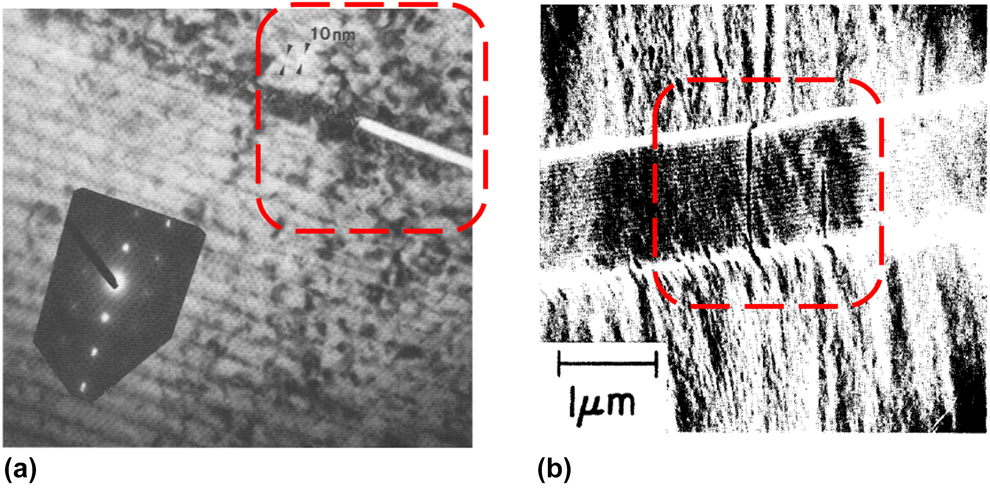
Early work on fracture in nanoscale metal–metal multilayered materials focused on cracks along the interface to understand the damage resistance or delamination between the layers during the fabrication of nanoscale multilayers. Lashmore and Thomson [Reference Lashmore and Thomson32] did early experimental work on the fracture of Cu/Ni multilayers of layer thickness 10 nm with a notch along the interface and observed misfit dislocation interactions between the predefined notch and multilayer interfaces around it as shown in Fig. 1(a). The generated misfit stresses amount to a giant Peierls friction stress with the deformation zone highly localized at the crack tip. The dislocations’ proximity around the crack tip suppressed continuous emissions, and this scenario favored a transition to a Mode II brittle, cleavage behavior through elastic theory and nonlinear atomistic modeling observations by Anderson et al. [Reference Anderson, Lin and Thomson33]. Matthew and Blakeslee [Reference Matthews and Blakeslee34] observed cracks across the interface at some areas of their fabricated GaAs/GaAs0.5P0.5 25 nm multilayered nanocomposite samples in Fig. 1(b). One of the cracks stopped at the interfaces by an array of misfit dislocations.
Examples of multilayered nanolaminates with cracks/notches (a) along the interface of Cu/Ni multilayered nanolaminates [Reproduced with permission from Cambridge University Press [Reference Lashmore and Thomson32]] and (b) across the interfaces of GaAs/GaAs0.5P0.5 25 nm multilayered nanocomposite. [Reproduced with permission from North-Holland Publishing Co. [Reference Matthews and Blakeslee34]] The area of interest is highlighted inside the red dotted box.

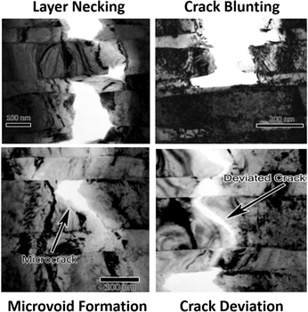
During in situ TEM tensile testing of Cu/Nb physical vapor deposited (PVD) 40 nm freestanding multilayered films along the layers, the material exhibits flow stress of 1.55 GPa and elongation to failure of 3.4%. Its fracture surface reveals evidence of ductile fracture with little necking occurring before failure with cracks along the grain boundaries within the layers [Reference Mara, Bhattacharyya, Hoagland and Misra35]. Hattar et al. [Reference Hattar, Misra, Dosanjh, Dickerson, Robertson and Hoagland36] observed the fracture behavior from an initial fabrication crack during the in situ TEM tensile straining experiment of Cu/Nb 60 nm/150 nm multilayers, and this fracture was attributed to CLS within the layers containing and preceding the crack tip. They observed four crack hindrance mechanisms—microvoid formation, crack deviation, layer necking, and crack blunting as shown in Fig. 2. The presence of the Cu/Nb interface influenced the location of the microvoids, redirection of the crack, the extent of necking along the crack path, and location of the crack blunting to take place mainly in the Cu layer close to the interface like obstacles.
Four crack hindrance mechanisms observed by Hattar et al. in Cu/Nb multilayered nanolaminates [Reproduced with permission from ASME [Reference Hattar, Misra, Dosanjh, Dickerson, Robertson and Hoagland36]].

So now, in a more systematic way, we want to extend the current knowledge of interfaces in nanoscale metal–metal multilayered materials on their roles in fracture and fatigue. It would be important and crucial to study interface interactions with a propagating crack in real time during fracture through in situ microfracture techniques. The effects of the constituent layer interfaces and grain boundaries on plasticity, fracture, and fatigue of the multilayers can be examined experimentally in real time and can be further evaluated theoretically or through simulations.
With the vision, overall goal, and justification of its scientific and technological merits in mind, this review will highlight the challenges in analyzing fracture in multilayers, the considerations for focused ion beam (FIB) fabrication, and the current examples that look into the fracture in multilayers.
Why analyze fracture in situ?
The in situ microfracture technique allows the simultaneous and synchronous recording of the load–displacement information, in addition to crack initiation and propagation events. The fracture load can be precisely noted, and the crack opening displacement (COD) can be determined via direct observation or digital image correlation (DIC) techniques [Reference Kammers and Daly37]. The development of instruments [Reference Doerner and Nix38, Reference Hay39] to both apply and measure loads and displacements accurately and observe the changes and record in situ [Reference Dehm, Jaya, Raghavan and Kirchlechner40] has enabled fracture testing of materials at micrometer and nanometer sizes to become a reality. Further, the availability of FIB machining, lithography, deep reactive ion etching (DRIE) and laser micromachining to prepare samples at small dimensions have encouraged the growth in this area.
Uniaxial loading in both tensile and compression modes have been done in situ for nanoscale metal–metal multilayered materials inside a scanning electron microscope (SEM) as well as TEM [Reference Li, Wang, Huang, Misra and Zhang15, Reference Hattar, Misra, Dosanjh, Dickerson, Robertson and Hoagland36, Reference Aydıner, Brown, Mara, Almer and Misra41, Reference Li, Mara, Wang, Dickerson, Huang and Misra42, Reference Mayer, Li, Mara and Chawla43, Reference Mara, Li, Misra and Wang44]. Results from these experiments have provided many insights into the plasticity mechanisms of multilayers at the nanoscale level due to interface interactions. However, these methods are not suitable for fracture studies. In the tensile mode, the maximum tensile stress is experienced throughout the entire volume of the testing sample, and fracture may not happen at the weakest direction for the crack driving force. If there are sources of weak grain boundaries or voids, lower values of fracture strength may be attained for the same material through tensile mode than through bending. In compression, the crack is aligned parallel to the compression direction. When the crack propagation is the controlling mechanism of failure, a larger amount of stress is required to fail a material in compression compared to tension. However, the maximum tensile stress is conversely concentrated in a small region on the top surface above the neural axis in bending mode, making it apt for fracture. Further, ASTM standard tests to measure crack propagation and fracture toughness in bulk materials are performed in bending only [45, 46].
Consequently, the conventional methods for evaluating fracture in materials in the bulk form cannot be applied such that new experimentation techniques are required in the micron and nanoscale levels. Researchers have proposed nonconventional solutions of single cantilever bending [Reference Alfreider, Kozic, Kolednik and Kiener47, Reference Allison, Moser, Schirer, Martens, Jordon and Chandler48, Reference Bohnert, Schmitt, Weygand, Kraft and Schwaiger49], double cantilever beam (DCB) [Reference Liu, Wheeler, Howie, Zeng, Michler and Clegg50], pillar splitting [Reference Sebastiani, Johanns, Herbert, Carassiti and Pharr51, Reference Sebastiani, Bemporad, Carassiti and Schwarzer52], and clamped beam bending [Reference Jaya, Bhowmick, Asif, Warren and Jayaram53, Reference Jaya and Jayaram54, Reference Jaya, Jayaram and Biswas55] to observe fracture in situ and allow for fracture toughness measurements for various kinds of materials. To identify key interface parameters enabling enhanced fracture and fatigue properties in nanoscale metal–metal multilayered materials, we would want to choose a method that is suitable for interfaces and allows us to view interface interactions with the notch and/or crack in situ in the line of sight, scalable at any length scale and a stable crack growth.
Sample preparation for In situ testing
In the past, researchers tend to peel away the film from the substrate after deposition to obtain just the multilayered film [Reference Mara, Bhattacharyya, Hoagland and Misra35, Reference Huang and Spaepen56]. This method was prone to create film samples of random sizes which were hard to control and keep for multiple uses. In recent years, the FIB has been used as a machining tool to modify materials at the micro- and nanoscale [Reference Allison, Moser, Schirer, Martens, Jordon and Chandler48, Reference Greer and De Hosson57, Reference Di Maio and Roberts58, Reference Jaya, Kirchlechner and Dehm59]. The FIB, also known as FIB, involves the use of a finely focused beam of ions inside an SEM to mill or sputter off materials or deposit materials in a particular location for specific applications. This technique saved fabrication time and provided more control over the beam and notch dimensions. As a result, FIB is used extensively in materials science [Reference Greer and De Hosson57, Reference Uchic, Shade and Dimiduk60, Reference Kraft, Gruber, Mӧnig and Weygand61, Reference Jaya and Jayaram62], biology [Reference Kizilyaprak, Daraspe and Humbel63, Reference Narayan, Danielson, Lagarec, Lowekamp, Coffman, Laquerre, Phaneuf, Hope and Subramaniam64], and the semiconductor industry [Reference Zschech, Langer, Engelmann and Dittmar65, Reference Giannuzzi, Drown, Brown, Irwin and Stevie66]. A liquid metal ion source, which can be gallium, helium, or xenon, is placed in contact with a tungsten needle, and the heated source wets the tungsten and flows to the tip of the needle. A Taylor cone is formed with the tip radius of ∼2 nm. The electric field around this small tip causes ionization and field emission of the metal ions. Based on the beam current setting, the FIB beam can be used for imaging and site-specific sputtering or milling. An extensive literature on how FIB can be used for mechanical structure fabrication can be found in the following Refs. Reference Dehm, Jaya, Raghavan and Kirchlechner40, Reference Jaya and Jayaram62, Reference Kiener, Motz, Rester, Jenko and Dehm67, Reference Uchic and Dimiduk68.
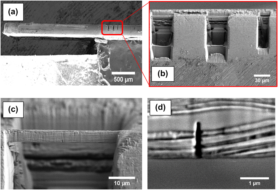
Figure 3 shows one such example of double clamped beams fabricated by FIB [Reference Radchenko, Anwarali, Tippabhotla and Budiman69]. Special care is taken to minimize the defect introduction from the FIB process. The top surface is polished to remove the inherent microcracks in the samples. Milling for many hours may be needed to release a film from the substrate. To minimize the milling ion exposure on the predefined notch at the center of the microbeam, a very low current is used to mill as one cut across the width of the beam.
Cu/Nb ARB beam made by FIB beam milling—(a) beams are made along the edge of the bulk sample circled with a red box. (b) 3 milled beams of various sizes in μm (l × b × t) (40 × 5 × 2), (40 × 5 × 4) and (20 × 5 × 2), (c) Closeup of one of the beams to check for defects and measurements (40 × 5 × 2) and (d) the sharp notch from this beam.

FIB is inherently a destructive technique to the specimen. When the high-energy ions bombard the sample, they will sputter atoms of the sample from the surface. The bombarding atoms (e.g., gallium) will also be implanted into a few nanometers from the surface, making the surface amorphous. Care needs to be taken to minimize the exposure of the milling as much as possible with a staggered milling process to make the structures and a final low voltage and current slow milling (or “polishing”) in the end. However, just like in any destructive process, the remnants from the milling process have to be deposited elsewhere. The milling steps such as the areas of interest (where we want to understand the effect of the interface on their mechanical properties) need to be planned such that the key areas do not get deposited with the remnants. Examples of critical areas include the front and back sides of the beam where we view the multilayered interfaces and crack propagation from the notch across the layers. Any presence of amorphous surface due to the deposited milled material on these critical areas affects the results and analysis.
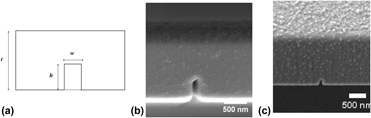
The accuracy of the FIB milling depends on the beam spot size at the surface being milled. An example is how the prenotch is created by a single cut across the beam of interest. However, this step results in the back notch being smaller in width and height than the front notch. If there is significant beam drift during the FIB milling, an uneven wide notch formation is formed instead of the expected sharp narrow notch for that particular beam.
There has been some studies on the effect of gallium (Ga+)-induced damage on the FIB milled microstructures and their plastic deformation mechanisms. The relative depth of ion penetration and damage in materials has been observed through experimentation and simulation [Reference Kiener, Motz, Rester, Jenko and Dehm67, Reference Bei, Shim, Miller, Pharr and George70]. For example, the penetration depth of 30 kV Ga+ ions in Cu is calculated to be ∼24 nm [Reference Kiener, Motz, Rester, Jenko and Dehm67]. Xiao et al. [Reference Xiao, Wehrs, Ma, Al-Samman, Korte-Kerzel, Gӧken, Michler, Spolenak and Wheeler71] recently investigated the effect of gallium as well as xenon ions on single crystalline and ultrafine-grained aluminum cantilevers and pillars. The minimal effect on the yield strength was observed for single crystalline aluminum samples, but gallium deposition along the grain boundaries of ultrafine-grained aluminum was observed and had a significant impact on the mechanical properties of the samples.
However, it is difficult to conclude that the effects observed in the in situ microfracture experiments can be influenced by the existence of the surface damage layer. Burek and Greer [Reference Burek and Greer72] did a comparison study of the mechanical behavior of gold and copper nanopillars made by FIB as well as electron beam lithography followed by electroplating. They did not observe any difference in the mechanical behavior between the two techniques due to the influence of Ga+ ion bombardment or electroplating technique for a broad range of diameter sizes. Other issues of the FIB milling technique include the rounding at the edges, different milling rates for heterogeneous materials, and a nonuniform foot geometry complicating the control and assessment of the final dimensions [Reference Hütsch and Lilleodden73]. Despite these concerns, FIB is being used extensively as the choice of method in the fabrication of micron test structures for in situ small-scale microfracture tests [Reference Dehm, Jaya, Raghavan and Kirchlechner40, Reference Alfreider, Kozic, Kolednik and Kiener47, Reference Lauener, Petho, Chen, Xiao, Michler and Wheeler74].
Once a crack starts to propagate in the beams upon loading, fracture mechanic concepts of linear elastic fracture mechanics (LEFM) for brittle materials or EPFM can be applied for nanoscale bulk materials depending on the load, crack length, and geometry of the tested structure [Reference Anderson and Anderson75]. However, for multilayers, this scenario is not as straightforward, taking into account the material inhomogeneity effect [Reference Simha, Fischer, Kolednik and Chen76].
The interface of multilayers can be a potential crack initiation site or a crack arrestor since the crack path depends on the orientation of the original crack with respect to the interface plane. The architecture of the multilayer structure at the nanoscale can be tweaked to enhance the crack resistance by metal combination, texture, grain size, coherency and growth strains, and defect distribution.
Take a scenario of a multilayer of two different metals, M1 and M2, where E M1 > E M2 and σy_M1> σy_M2. The alternating stacking of M1 and M2 metal layers will bring out sharp gradients in the residual stress along with the elastoplastic property mismatch along the coating cross-section [Reference Dauskardt, Lane, Ma and Krishna77, Reference Erdogan78, Reference Hutchinson and Evans79]. As the crack tip travels across an interface from M1 to M2, the crack is able to propagate across due to the anti-shielding effect. However, if the crack travels to a subsequent layer from M2 to M1, crack propagation is hindered and the crack tip experiences a shielding effect [Reference Simha, Fischer, Kolednik and Chen76, Reference Simha, Fischer, Kolednik, Predan and Shan80].
As the test structures shrink in size especially in the width and notch height, the necessary stress to generate a dislocation at a crack tip becomes very high, significantly larger than the typical yield stress of a coarse-grained metal or alloy. The far-field stress will decrease to a lesser extent compared to the elastic stress field. As a result, dislocation sources become fewer and those dislocations being generated may escape from the sample too.
The way the test structures are loaded and tested will affect the fracture behavior, especially in EPFM. When tested in bending, besides the multilayered structure arrangement, the dislocation movements will be controlled by the dislocation pile-up at the neutral axis of the bending [Reference Wurster, Motz, Jenko and Pippan81]. The extent of dislocation pile-up will not only be dependent on the sample size but also on the orientation of the dislocation glide plane(s) within the sample [Reference Motz, Schӧberl and Pippan82, Reference Kapp, Kirchlechner, Pippan and Dehm83]. The dislocations in front of the crack will be densely packed. However, if tested in tensile, there will be the influence of the multilayers but little on the influence on the crack tip due to the loosely packed arrangement.
ASTM standard fracture mechanics tests have been established for 10 mm and above structures [45, 46]. However, they are not suitable at the micro- and nanoscale. The size of the plastic zone around the crack tip influences the fracture behavior [Reference Anderson and Anderson75]. If the plastic deformation and opening (CTOD) occur within the K-dominated zone, small-scale yielding with the use of LEFM is performed to calculate the fracture toughness of materials. However, if the size of the plastic zone exceeds the K-dominated zone, EPFM is used to describe the stress and strain behavior in front of a crack. One can refer to Dehm et al. [Reference Dehm, Jaya, Raghavan and Kirchlechner40] for the specific LEFM and EFEM equations that can be used. This technique of the J-integral is established for homogeneous materials [45], but not so much for heterogeneous materials for multilayered systems [Reference Zechner and Kolednik84].
Progress is also being made in modeling such as interfaces and studying their fracture behavior via simulations. To quantify the dislocation activities around the crack tip, crystal plasticity or molecular dynamics models are required to analyze the stress the deformation behavior in front of the crack where the relevant fracture processes take place. The dislocations generated usually reduce the elastic stress field at the crack tip—dislocation shielding. Dislocations can also increase the local elastic field depending on their Burgers vector and position—anti-shielding—and may induce decohesion at the crack tip. Hence, the crack tip shielding in microsamples can be different from that of observed in macrosamples. This should result in a sample size-dependent fracture resistance controlled by the interplay between the slip distance, specimen dimensions, and the extent of the K-dominated zone. The arrangement of the dislocations and the extent of the dislocation-free zone can be affected by the sample size and loading type.
With this understanding, is only in situ techniques will enable us to see changes in fracture mechanisms with reducing the thickness of individual layers in multilayered nanolaminates, where the process zone begins to overlap between two or more layers simultaneously. As shown in the examples, multilayering in the nanoscale is not a straightforward but evolving optimization process.
Highlights from recent advances in In situ fracture
Fracture upon tensile testing of film on a substrate
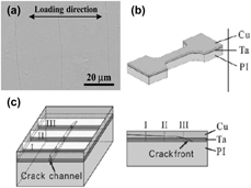
With the increasing trend in flexible electronics and paper-like displays, there was a need to study the plastic deformation and cracking behavior of the multilayered film that could be adhered to a polymer substrate. It has been demonstrated that such a film/polyimide composite could be used to investigate plastic deformation and cracking behaviors by applying a certain strain to the composite [Reference Macionczyk and Brückner85, Reference Xiang, Li, Suo and Vlassak86]. The group by Zhang investigated how the plastic deformation is localized and cracks initiate from the localized damage regions in nanoscale Cu with FCC/BCC/HCP metal (called X) multilayers bonded to flexible polyimide substrates [Reference Zhang, Zhu, Tan and Liu87, Reference Zhu and Zhang88, Reference Li, Tan and Zhang89, Reference Li and Zhang90, Reference Zhu, Li, Zhang, Tan and Liu91, Reference Zhu, Zhang, Yan, Zhu and Sun92, Reference Zhang, Liu, Wang and Tan93, Reference Li, Kreuter, Luo, Schwaiger and Zhang94, Reference Li, Zhang, Wang, Tan and Zhu95, Reference Yan, Zhu, Yang and Zhang96, Reference Li, Zhu, Tan, Wu and Zhang97]. Upon tensile testing of the dog bone sample, the sample is examined in situ to understand the microfracture and mechanisms behind the fracture of the multilayered metallic films.
Equal layers of Cu and X are deposited by radio frequency (RF) magnetron sputtering system under a high vacuum base pressure of 1 × 10⁻⁷ torr onto a 125-µm-thick polyimide substrate. The total thickness of the deposited multilayer is about 1 µm. They investigated a wide range of individual layer thicknesses from 1 to 250 nm. The composite is then reshaped to a tensile dog bone with a gauge section of 15 mm in length and 5 mm in width as shown in Fig. 4(b). The tensile test is performed using a microforce testing machine at a constant strain rate of 1.6 × 10⁻⁴ s−1 up to 5% strain, and then the samples were unloaded. The amount of strain was accurately measured by the extensometer or electrical resistance method, R. The critical strain, εc, was recorded, defining the inflexion point between a linear and nonlinear change in resistance due to the presence of voids and cracks. The Young’s modulus and yield strength of the film from the film/substrate system can thus be calculated from the following equations [Reference Yu and Spaepen98, Reference Avilés, Llanes and Oliva99]:
 $${E_{\rm{f}}} = \left( {{{{t_{\rm{s}}}} \!\left/{\vphantom{{{t_{\rm{s}}}} {{t_{\rm{f}}}}}}\right.{{t_{\rm{f}}}}}} \right)\left( {{E_{{\rm{total}}}} - {E_{\rm{s}}}} \right)\quad ,$$
where E f, E s, and E total are the Young’s moduli of the film, substrate, and total film/substrate system, respectively. t f and t s are the thicknesses of the film and substrate, respectively.
 $${\sigma _{\rm{f}}} = \left( {{{{t_{\rm{s}}}} \!\left/{\vphantom{{{t_{\rm{s}}}} {{t_{\rm{f}}}}}}\right.{{t_{\rm{f}}}}}} \right)\left( {{\sigma _{{\rm{total}}}} - {\sigma _{\rm{s}}}} \right)\quad ,$$
where σf, σs, and σtotal are the Young’s moduli of the film, substrate, and total film/substrate system, respectively.
(a) SEM image of the surface of the Cu/Ni multilayered film after the tensile test experiment. [Reproduced with permission of Taylor & Francis [Reference Zhu, Zhang, Yan, Zhu and Sun92]]. (b) Design of the dog bone-shaped tensile sample of the multilayered film on a polyimide substrate. (c) Schematic illustration of the damage zone ahead of a channel crack in the out-of-plane direction which is cross-sectioned at positions I, II, and III. To understand the multilayered film fracture, in particular, a position I is chosen. [(b) and (c) Reproduced with permission of Cambridge Core [Reference Zhu, Zhang, Tan, Liu and Zhu100]].

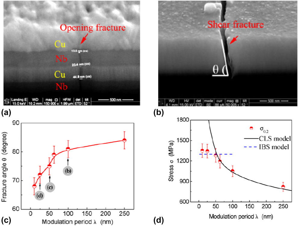
After the tensile test, some cracks formed in the multilayer and grew along the direction almost perpendicular to the loading axis as shown in Fig. 4(a). FIB cross-sectioning was done at specific locations of interest as shown in Fig. 4(c) to understand the localized deformation across the multilayers. They observed the resultant fracture angle between the macrocracking direction and the horizontal direction as well as the extent of the crack across the layers. Respective SEM images are often shown after that to characterize the fracture behavior as shown in Figs. 5(a) and 5(b).
Different fracture profiles as the individual nanolayer decreases for Cu/Nb multilayered nanolaminates from (a) an opening fracture at h = 125 nm to (b) a shear fracture at h = 5 nm [(a) and (b) Reproduced with permission from Elsevier [Reference Zhang, Zhang, Wang, Lei, Zhang, Niu, Liu, Zhang and Sun101]]. (c) Dependence of theta on λ for the Cu/Cr multilayered films with η = 1. (d) Dependence of stress σ0.2 on λ for the Cu/Cr multilayers with η = 1 where the solid curve is calculated from the CLS model and the dash curve is from the IBS model [(c) and (d) Reproduced with permission from Elsevier [Reference Zhang, Zhang, Liu, Zhang and Sun102]].

From these studies, they developed a rationale between the trend of fracture at different individual layer thicknesses and theorize them with the known dislocation plasticity mechanisms of Hall–Petch relation, CLS, and dislocation crossing across the layers. A large resultant fracture angle with a brittle fractography represented a thicker (>50 nm) individual layer thickness, whereas a smaller fracture angle represented a ductile shear fracture as shown in Figs. 5(c) and 5(d). They could also quantify the K IC at the notch tip to determine the stresses and trend of fracture. The cracking of brittle films was described analytically with 2D steady-state models, in which the steady-state energy release rate, ξ, can be described as follows [Reference Zhang and Zhang103]:
 $$\xi = {{\pi {\sigma ^2}{t_{\rm{f}}}} \over {2E}}\left( {1 - {\nu ^2}} \right)g\left( {\alpha ,\;\beta } \right)\quad ,$$
where E is the Young’s modulus of the multilayered nanocomposite, ν is the Poisson’s ratio, σ is the tensile stress at critical strain, t f is the total multilayer thickness, and g(α, β) is a dimensionless quantity with α and β being the two Dundurs’ parameters [Reference Dundurs and Mura104].
The fracture toughness (K IC) is thus expressed as follows [Reference Was and Foecke105]:
 $${K_{{\rm{IC}}}} = \sqrt {{{E\xi } \over {1 - {\nu ^2}}}} \quad .$$
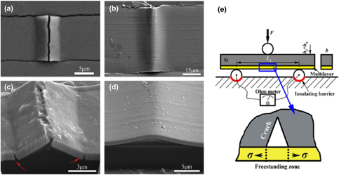
If strained further till 20%, compressive transverse stresses arise in the film due to a Poisson’s ratio mismatch between the substrate and film. The compressive stresses will cause buckling and delamination of the film. The interfacial adhesion energy can be measured from the buckled geometry and film thickness as shown in Figs. 6(a)–6(d) [Reference Wu, Zhang, Liu, Zhang, Cheng, Li, Zhang and Sun106].
Respective SEM images showing (a) cracked buckle in the Cu/Nb multilayers and (b) a faultless buckle in the Cu/Zr multilayers, (c) the buckles in Cu/Nb multilayers crack not only at the top but also the base (marked by arrows). (d) The buckles in Cu/Zr multilayers are symmetrical and have a smooth arch shape. [Reproduced with permission from Elsevier [Reference Wu, Zhang, Liu, Zhang, Cheng, Li, Zhang and Sun106]]. (e) Schematic illustration of three-point bending apparatus used for localized fracture experiment. [Reproduced with permission of Elsevier [Reference Li and Zhang90]].

For Cu/Ta and Cu/Ni on polyimide substrates, fatigue tests were also performed under load control between a maximum tensile load and a constant minimum tensile load of 0.2 N at a frequency of 20 Hz with the same setup. After 1 × 10⁶ cycles were completed at a specific load range, the samples were checked by an SEM. If there was no fatigue damage observed at the specimen surface, P m was raised to a higher level until fatigue damage could be observed on the specimen surface by the SEM within 1 × 10⁶ cycles. The trend observed is similar to that of the yield strength of multilayers. The higher the nominal fatigue strength, the lower the individual spacing.
In one of their papers, the use of three-point bending tests on the multilayered film/polyimide substrate system for Cu/Au and Cu/Cr multilayers was investigated [Reference Li and Zhang90] as shown in Fig. 6(e). A brittle 525-µm-thick Si(100) single crystal was selected as the substrate to ensure substrate cracking before multilayer fracture. The bending span was set as 6 mm, and the width of all specimens was 1.2 mm. Static bending tests were conducted. Manufacturing a precrack, loading to induce crack propagation, measuring the critical stress needed to inflict fracture, and observing the fracture morphology is followed by a simple procedure to conduct.
During the bending process, the critical energy release rate equation [Reference Jaeger, Endler, Heilmaier, Bartsch and Leonhardt107], ξc, can be calculated, knowing the compliance, C, and crack length, r:
 $${\xi _{\rm{c}}} = - {{{\rm{d}}{U_{\rm{e}}}} \over {{\rm{d}}{A_{\rm{c}}}}} = - {{{1 \over 2}\Delta {F^2} \cdot {\rm{d}}C} \over {2{t_{\rm{f}}} \cdot {\rm{d}}r}}\quad ,$$
where U e is the elastic energy, A c is the area of the crack, t f is the film thickness,  ${{{\rm{d}}C} \over {{\rm{d}}r}}$ is the change in the compliance of the film with respect to the change in crack length, and ΔF is the measured force difference. The fracture toughness, K c, of the multilayer of Young’s modulus, E, can be thus calculated as:
 $${K_{\rm{c}}} = \sqrt {E{\xi _{\rm{c}}}} \quad .$$
The multilayer must be thin enough relative to the substrate in order to eliminate the effects of stress nonhomogeneity at the crack tip. The effects of the constituent layer scales, layer interfaces, and grain boundaries on plasticity and fracture of the multilayers were examined experimentally and evaluated theoretically.
As expected, a crack preferentially initiated in the middle of the Si substrate, close to the film/substrate interface due to the maximum tensile stress, and then a local free-standing multilayer was produced ahead of the opening crack. Thus, plastic deformation of the free-standing multilayer subject to tensile stress continued with substrate crack opening until final rupture of the multilayer/substrate system. This method was a slight improvement over the tensile method.
Interface shear strength determination through clamped beam bending
As seen in the previous section, performing mechanical experiments in the tensile mode until fracture is the easiest way to understand fracture mechanisms in multilayers. However, the formation of cracks in the sample becomes random such that it becomes challenging to analyze the fracture quantitatively. An alternate fracture test geometry needed to be explored to analyze fracture across the multilayers.
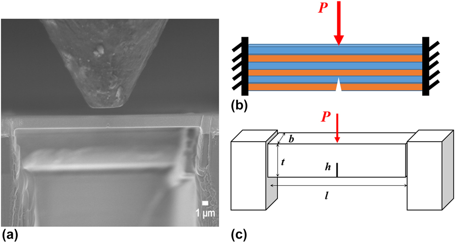
Clamped beam bending was first demonstrated as a fracture test geometry at the nanoscale on PtNiAl bond coats [Reference Jaya, Jayaram and Biswas55]. It is based on a modification over the three-point bend test by clamping the ends instead of letting them free as shown in Fig. 7. The concept of in situ microfracture clamped beam bending for fracture across metal–metal multilayers was presented by Budiman as an invited talk in the International Conference on Plasticity, Damage and Fracture 2017 [Reference Budiman108]. Since then, two works by Radchenko et al. [Reference Radchenko, Anwarali, Tippabhotla and Budiman69] and Anwar Ali et al. [Reference Anwar Ali, Radchenko, Li and Budiman109] have been published with the help of this technique.
(a) SEM image of clamped beam bending geometry for nanoscale PVD metal–metal multilayered composite where the beam is made by FIB. A conical flat tip of 5 µm diameter is used to load the beam. (b) Schematic representation of the clamped beam bending geometry with a notch across the layers and (c) 3D model representation of the clamped beam bending geometry with the beam dimensions.

Within elastic limits, simply supported beams deform four times more than rigidly clamped ones [Reference Timoshenko110]. A clamped beam offers a more stable setup with crack arrest after a certain amount of propagation from the notch tip. The position of the maximum principal tensile stress changes from the notch tip to the fixed ends once the h/t ratio of the crack exceeds ∼0.5 [Reference Jaya and Jayaram54, Reference Jaya, Jayaram and Biswas55]. This transition makes the clamped beam bend configuration transform from an unstable to a stable system for crack propagation.
The beam dimensions made by FIB should adhere to an l/t ratio between 4 and 8 and an initial h/t ratio between 0.3 and 0.5 based on satisfying both plane strain and small-scale yielding criteria [Reference Jaya, Kirchlechner and Dehm59, Reference Iqbal, Ast, Gӧken and Durst111]. A much shorter or longer starting crack length will not provide stable crack growth and also give rise to free surface effects. The notch sizes (h × w) in all beams are varied due to the challenging process of creating these notches by FIB as a single cut across the beam as shown in Fig. 8. The width of the notch, w, is to be as small as possible to almost a knife edge (i.e., 100–300 nm range).
Sharp notches made by FIB: (a) schematic of a notch of width, w and height, h in the microbeam of thickness t, (b) SEM image of the front notch of h = 400 nm and w = 120 nm, and (c) SEM image of the back notch which is smaller than the front notch [Reproduced with permission from Elsevier [Reference Anwar Ali, Radchenko, Li and Budiman109]].

The in situ mechanical experiments are carried out inside the JEOL FESEM (JSM-7600F) using a PI-85 SEM picoindenter (Bruker Inc., Minneapolis, Minnesota) with a 20 mN maximum load transducer. Two beams were tested for each material system. The beams were loaded using a conical flat tip of 5 µm diameter and carried out in displacement control mode. A constant loading displacement rate of 5 nm/s with a Q-control of 0.2, an integral gain of 0.2, a derivative gain of 1, and a specific preload was maintained for all experiments. The load–displacement data and the real-time video of the experiments were synchronized and captured during the experiment using a frame grabber with the TriboScan software (Bruker Inc.). Care was taken to perform drift correction before the experiment started and corrected to the final load–displacement measurements.
This geometry offers pure mode I loading as well as controlled mixed mode loading by placing the indenter at fixed offsets from the notch position. The crack can be seen to grow and arrest in stages before complete failure ensues. Such controlled crack growth is important in the measurements of R-curve or fatigue behavior of materials [Reference Jaya and Jayaram54, Reference Jaya, Kirchlechner and Dehm59] as well as in following crack trajectory and study of toughening mechanisms after the experiment.
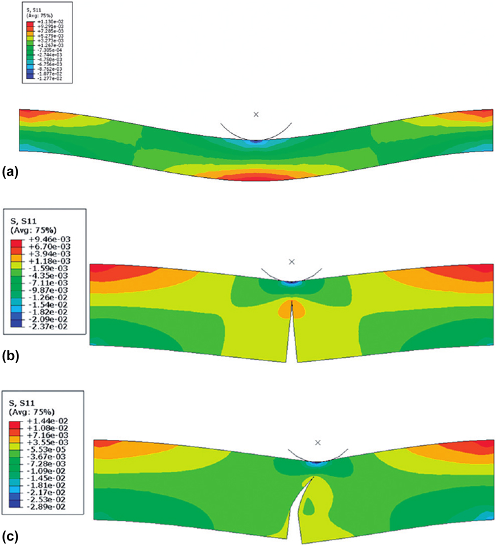
Jaya et al. [Reference Jaya, Jayaram and Biswas55] did FEM models of the clamped beam geometry for PtNiAl bond coats as shown in Fig. 9. The unnotched beam showed maximum tensile stress occurring at both fixed ends and bottom edge center. If the tip was aligned with the notch correctly, the crack was seen to propagate in mode I in the direction of maximum tangential stress toward the loading line. If the tip was offset away from the notch, the crack tended to follow the loading line but did not significantly change the fracture mode based on their extended finite element method (XFEM) results [Reference Jaya, Jayaram and Biswas55]. Cracks were only observed at the edges when the beams are overloaded.
Stress contour plots at a specific load of P = 0.75 N using beam specification of PtNiAl bond coats, showing positions of maximum tensile stress S11 and crack trajectories for mode I and mixed mode cases—(a) unnotched beam in bending, (b) 0 µm load offset and (c) 5 µm load offset [Reproduced with permission from Taylor & Francis [Reference Jaya, Jayaram and Biswas55]].

The maximum principal stress that opens up the crack acts along the line connecting the notch tip and the indenter. Therefore, the indenter should ideally be positioned precisely across the notch for mode I loading, but misalignments up to 5% of beam length are tolerable. The indenter tip should be sufficiently blunt not to cause indentation impressions or cracking. The test is no more valid if and when edge cracking initiates at the clamped ends. Maintaining larger l/t ratios prevents edge cracking. K I is obtained via XFEM simulations and has a sinusoidal dependence on h/t. Though the general form of this dependence remains constant for this geometry, each case differing in sample dimensions has to be separately simulated for quantitative determination of K I in the absence of readily available analytical solutions [Reference Jaya, Bhowmick, Asif, Warren and Jayaram53, Reference Jaya and Jayaram54]. If there are cracks greater than the notch height present at one or both edges, the clamped beam might fail prematurely [Reference Jaya and Jayaram54].
One might question why not to use single cantilever beams instead of clamped beam geometry to measure the stresses and quantify the resulting K I. Single cantilever beams are inherently unstable loading systems subjected to maximum shear during the initial loading, and the extent of shear to tensile mode drops off at later time steps. Catastrophic failure of the beams occurs, preventing the extraction of information post-mortem. The point of contact does not remain constant since the position is displaced due to the large displacement of the beam in the vertical direction. Hence, the span length becomes variable. Load offsets cannot be quantified easily with single cantilever beams too. However, there have been attempts to use notched cantilever beams to study fracture in multilayered nanocomposite beams [Reference Alfreider, Kozic, Kolednik and Kiener47, Reference Kozic, Gänser, Brunner, Kiener, Antretter and Kolednik112, Reference Treml, Kozic, Schӧngrundner, Kolednik, Gänser, Brunner and Kiener113].
There are challenges in performing fracture toughness values to determine the critical stress intensity factor, K IC or J-integral. This is especially so for clamped beam bending geometry where there is a lack of analytical formulation for K I. Since K I does not follow a monotonically linear relationship with increasing h/t ratio, FE modeling is performed to calculate K I [Reference Jaya, Bhowmick, Asif, Warren and Jayaram53, Reference Jaya and Jayaram54, Reference Jaya, Jayaram and Biswas55]. Standard geometries used to determine fracture toughness such as single edge notch bend (SENB) [45] cannot be scaled down easily due to limitations in specimen size and instrumentation. It is complicated to obtain a free-standing thin film specimen mounted on roller supports to replicate SENB test. That is why nonstandard geometries such as single cantilever and clamped beam geometries are used.
Further, the fatigue starter cracks or notches of the microbeams are made with FIB [Reference Dehm, Jaya, Raghavan and Kirchlechner40]. Since the fracture toughness is sensitive to the material composition, there is a concern of the material around the crack tip to be significantly altered by ion implantation. As the dimensions of the beam specimen shrink into the micro- and nanoscale, the crack tip plastic zone becomes a more significant fraction of the specimen dimension, while also interacting with the free surface and indentation-affected zone.
Another interesting part of Cu/Nb accumulative roll-bonded (or ARB) multilayered nanolaminates is that they have a large anisotropy of the interface shear strength between the rolling (RD) and transverse (TD) directions. To study this effect, Radchenko et al. [Reference Radchenko, Anwarali, Tippabhotla and Budiman69] studied the effect of interface shear strength on the failure in Cu/Nb 63 nm ARB multilayered nanolaminates using the in situ clamped beam bending microfracture technique experimentally based on molecular dynamic results by Demkowicz and Thilly [Reference Demkowicz and Thilly114].
The results showed a substantial difference between the fracture behaviors along the RD and TD owing to differences in the interface shear strength and grain size. The maximum relative notch width which was increased before crack initiation was between 50 and 100% for the RD beams and exceeded 400% for the TD beams depending on the material of layer at the notch tip. Through confirmation of the stresses with FEM [Reference Radchenko, Anwarali, Tippabhotla and Budiman69], they identified that the notch widening is due to plasticity for the RD beams, whereas the influence of interface shear is prevalent in TD beams.
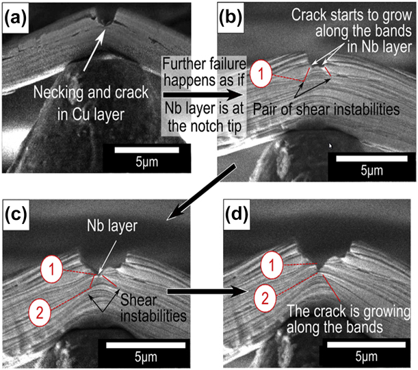
The in situ technique provided insights into identifying the specific material (Cu or Nb) influencing the notch widening and eventual fracture across the beam as shown in Fig. 10. The material was identified from the low angle backscattering emission (LABE) SEM images. Shear instabilities were formed when the Nb layer was at the notch tip followed by crack initiation. If the Cu layer was at the notch tip, necking and crack happened at the Cu layer followed by slip bands and crack initiation at the subsequent Nb layer. The intricate details of the fracture were captured all due to the in situ technique. Thus, the slip bands originated from the Nb layers at the notch/crack tip in the RD beams followed by crack propagation along these bands.
Crack initiation and propagation in the rolling direction (RD) beam that varies depending on the layer material (Cu or Nb) on the notch tip. The example shows if Cu was at the notch tip. (a) After some notch widening, necking occurred with a crack initiation. (b) As the crack propagates, a shear instability is formed in the subsequent Nb layer, and the crack starts to grow along the bands in the Nb layer. (c) The crack propagates along one of the shear instabilities until the end. (d) The crack continues to propagate along one of the shear instabilities toward the loading line until it becomes close to the beam surface. [Reproduced with permission from Elsevier [Reference Radchenko, Anwarali, Tippabhotla and Budiman69]].

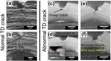
For the TD beams, the crack propagation is inhibited by interface shear. We suggest that shear bands form subsequently through the beam and lead to the final beam failure. Though the FE simulations for the TD beams show the similar result through complication in the beam stress evolution [Reference Radchenko, Anwarali, Tippabhotla and Budiman69], it could not capture one of the actual experiment beam cases of crack initiation as shown in Fig. 11. The influence of the grain boundary at the notch tip resulted in a sharp microcrack formation with limited notch widening to failure. The interface shear in the TD beams could not be inhibited due to the presence of the grain boundaries near the stress concentration zone. The crack growth can be attributed to the formation of microcracks at the grain boundaries besides the main crack. Further, the differences in shear instabilities between RD and TD beams were only understood through the videos of the in situ testing. Post-fracture beams might not have captured all the in between events and result in just speculation.
Crack initiation and propagation in the TD beams. (a) The crack initiates in the middle of the notch followed by (b) an interface shear for most of the tested beams. However for one of the beams, (c) a sharp crack initiation in the layer at the notch tip with no significant interface shear. (d - e) This is followed by the microcrack formation in the Nb layer besides the main crack. (f) The main crack and microcrack are then connected via shear with the main crack growing through the Cu layer. [Reproduced with permission from Elsevier [Reference Radchenko, Anwarali, Tippabhotla and Budiman69]].

Influence of fabrication technique on the FCC/BCC interface role in fracture
Nanoscale metal–metal multilayered materials are known to be fabricated by physical vapor deposition (PVD) or sputtering. However, they can also be made by the top-down process of accumulative roll bonding (ARD). Not much work has been done to look into the differences in the interface interactions of crack propagation in real time in nanoscale metal–metal multilayered materials made by these two fabrication processes. Cu/Nb nanolayers of the similar individual layer thickness of 20 nm are chosen based on the vast literature of its elastic and plastic properties.
Through the in situ technique as mentioned in Interface shear strength determination through clamped beam bending, the fracture of the beams across the multilayers can be observed instantaneously. It was unexpected to observe a sudden catastrophic brittle fracture for the Cu/Nb PVD beams as shown in Fig. 12(a). A linear elastic load–displacement curve was observed up to the maximum load before a sudden breakage across the layers. Further, from their in situ video, no sign of slip band or shear instability being formed before the fracture is observed unlike what was observed in the Cu/Nb micropillar compression (successive ex situ micropillar compression) of the similar layer thickness [Reference Budiman, Han, Li, Wei, Dickerson, Tamura, Kunz and Misra22, Reference Budiman, Narayanan, Li, Wang, Tamura, Kunz and Misra23]. The presence of the multilayers did not attempt to stop the fracture. The fracture only lasted 1–2 frames. Thus, the Cu/Nb PVD beams fractured before yielding along the columnar grain boundaries.
(a) Cu/Nb PVD beam’s catastrophic fracture is observed at the end of the test with the crack propagating nearly parallel to the direction of the applied load across the full beams. (b) Notch widening is observed for the Cu/Nb ARB beam. Initial crack from the back of beam while the notch is widening. (c) The crack starts to propagate and tear through the beam with a shear instability is formed at the end of the crack tip, resulting in a ductile fracture. [Reproduced with permission from Elsevier [Reference Anwar Ali, Radchenko, Li and Budiman109]].

More interesting fracture events leading to crack tip blunting effects were observed for the Cu/Nb ARB multilayered beams. The Cu/Nb ARB beams experience significant fracture events such as notch widening, crack initiation and propagation, and final fracture along shear instability as shown in Figs. 12(b) and 12(c). The large notch widening in the beams is due to the plastic dislocations emitting within the layers below the notch tip, attempting to blunt the crack tip [Reference Hsia, Suo and Yang115]. The dislocations are able to be emitted in the absence of confinement away from the crack tip, lowering the stress at the crack tip and suppressing cleavage as much as possible.
These phenomena can be attributed to the differences in the interfaces and grain sizes and shapes created by the different fabrication paths of the same Cu and Nb multilayers. However, further detailed examinations of both fracture behaviors of the materials at the nanoscale levels showed competing mechanisms between individual grain structures and interface properties during the fracture of the nanoscale multilayered materials.
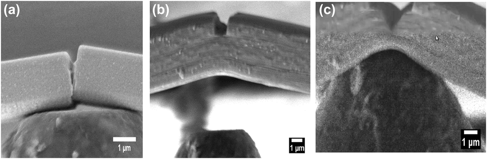
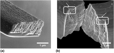
The Cu/Nb ARB beams experience significant fracture events such as notch widening, crack initiation and propagation, and final fracture along shear instability. The large notch widening in the beams is due to the plastic dislocations emitting within the layers below the notch tip, attempting to blunt the crack tip as shown in Fig. 13(b) [Reference Hsia, Suo and Yang115]. The dislocations are able to be emitted in the absence of confinement away from the crack tip, lowering the stress at the crack tip and suppressing cleavage as much as possible. In a layered material, the dislocations are confined by the adjacent, less ductile layers. These confined dislocations send back stress to the crack tip which impedes further dislocation emission [Reference Hsia, Suo and Yang115]. The applied stress intensity is increased after some extent of blunting till it reaches the cohesive strength of the layers in the multilayered beam. The ARB multilayered beam starts to fail by necking with a crack formation and cleavage fracture. Thus, the crack initiated from the back propagated through the beam. Once the plastic zone approached the bottom of the beam, the tip of the notch started to interact with it. This interaction can be associated with the formation of shear instability as shown in Fig. 12(c). The ARB interface, which is known to have a high interface shear strength compared to the PVD interface, permits slip transmission and thus promotes nearly crystallographic slip bands [Reference Zheng, Wang, Carpenter, Mook, Dickerson, Mara and Beyerlein116]. The crack continued to grow along the shear instability. This crack extended all the way through the remaining beam thickness to its final failure. A similar shear band failure was also observed during the microcompression of Cu/Nb ARB pillars [Reference Snel, Monclús, Castillo-Rodríguez, Mara, Beyerlein, Llorca and Molina-Aldareguía117]. As a result, a ductile fracture was observed for the Cu/Nb ARB beams due to the dislocation plasticity behavior at the Cu/Nb ARB interface confirmed from the fractography in Fig. 13(b).
(a) The fractured Cu/Nb PVD beam cross section shows the crack propagating through the columnar grains. (b) Fracture profile of the broken Cu/Nb ARB 4-µm-thick beam from the inside. The notch widening is observed at the edges highlighted by the white boxes with arrows. [Reproduced with permission from Elsevier [Reference Anwar Ali, Radchenko, Li and Budiman109]].

In contrast with the Cu/Nb ARB beams as described above, the Cu/Nb PVD beams experienced a sudden catastrophic fracture event, typical of brittle fracture in the present experiment. In earlier nanoindentation [Reference Mara and Beyerlein20] and micropillar compressions [Reference Mara, Bhattacharyya, Dickerson, Hoagland and Misra18, Reference Mara, Bhattacharyya, Hirth, Dickerson and Misra19, Reference Budiman, Han, Li, Wei, Dickerson, Tamura, Kunz and Misra22, Reference Budiman, Narayanan, Li, Wang, Tamura, Kunz and Misra23, Reference Mara, Bhattacharyya, Dickerson, Hoagland and Misra118] experiments using Cu/Nb multilayered nanolaminates, significant plasticity in the Cu/Nb nanoscale multilayered materials was observed due to the influence of the multilayered interface. Thus, at 20 nm layer thickness, the Cu/Nb PVD beams fractured before yielding along the columnar grain boundaries. The fractography of Cu/Nb PVD multilayered film in Fig. 13(a) shows the availability of grain boundaries through the columnar grain layers for the crack to extend along the grain boundaries. Both layers had a small grain size which made it difficult to deform by dislocation sliding. The columnar grains in Cu and Nb layers were aligned, forming an almost perpendicular fracture path to the tip loading condition [Reference Mara, Bhattacharyya, Hoagland and Misra35]. Due to the stress concentration and loss of the interface barrier at the crack tip, the deformation was confined to a local area which severely limited the plasticity of both Cu and Nb layers. Similar observations were made for Cu/Cr multilayered films [Reference Li and Zhang90]. The sites of crack initiation became random due to the inhomogeneous distribution of the cohesive strength of the columnar grain boundaries, which lead to the formation of the grain-sized steps or cavities at the fracture surface of Cu/Nb PVD beams.
Delamination along the multilayered interface
The simplest approach to understand the delamination of a particular interface is to perform nanoindentation tests to calculate the interfacial fracture energy by determining the buckle geometry around the indents. However, not all the interfaces will buckle upon indentation. Other explored methods include notched microcantilevers [Reference Matoy, Schӧnherr, Detzel, Schӧberl, Pippan, Motz and Dehm119] and DCBs [Reference Liu, Wheeler, Howie, Zeng, Michler and Clegg50] to understand delamination or adhesion between two layers of the nanoscale metal–metal multilayers. However, all these techniques will test the weakest of all the interfaces in the multilayer stack with little control over the interface of interest. Kiener et al. [Reference Kozic, Gänser, Brunner, Kiener, Antretter and Kolednik112, Reference Treml, Kozic, Schӧngrundner, Kolednik, Gänser, Brunner and Kiener113, Reference Treml, Kozic, Zechner, Maeder, Sartory, Gänser, Schӧngrundner, Michler, Brunner and Kiener120] found a more systematic way to understand the propagation of a crack along the layers using notched cantilever beams.
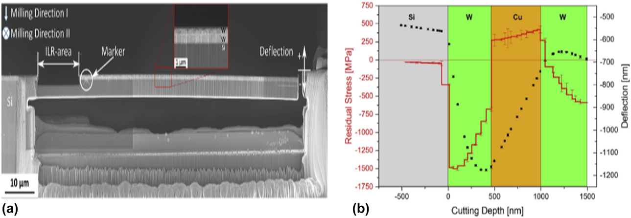
Before the actual in situ fracture experiment, residual stresses and stress gradients were measured through an improved ion beam layer removal (ILR) method [Reference Treml, Kozic, Zechner, Maeder, Sartory, Gänser, Schӧngrundner, Michler, Brunner and Kiener120, Reference Massl, Keckes and Pippan121]. Cantilevers were prepared from single-, bi- and tri-layer systems with an individual layer thickness of 500 nm using FIB machining. Subsequently, residual stress profiles were determined with a depth resolution of 50 nm, employing the ILR method.
To determine the stress profile, the cantilever is cut free on one side, and the thickness of the film in the rear part of the sample, called ILR area with a length of approximately 15 μm, is reduced gradually using the FIB. Thus, the curvature changes in the ILR area. The rest of the cantilever stays unaltered and acts as an amplifier for this curvature. The cantilever deflection is measured at the tip. Due to stress redistribution, this deflection changes gradually with each step of thickness reduction [Reference Massl, Keckes and Pippan121, Reference Schӧngrundner, Treml, Antretter, Kozic, Ecker, Kiener and Brunner122]. The evaluated film stresses in an individual layer depends on the layer order and can be tensile or compressive. An example of a residual stress profile is W–Cu–W done by Treml et al. [Reference Treml, Kozic, Zechner, Maeder, Sartory, Gänser, Schӧngrundner, Michler, Brunner and Kiener120] as shown in Fig. 14. As single layers deposited on a silicon substrate at room temperature, both W and Cu exhibit compressive behavior on silicon. However, in the combination of W–Cu–W, the residual stress profile changed from compressive to tensile when transiting from W to Cu with pronounced stress gradients. This technique highlighted the need to consider residual stresses in cantilever beams together with the substrate.
(a) The cantilever beam with the multilayered (W–W) film on top with the indication of the ILR area close to the support. (b) Deflection and residual stress profile of a W–Cu–W multilayer on a Si substrate. [Reproduced with permission from Elsevier [Reference Treml, Kozic, Zechner, Maeder, Sartory, Gänser, Schӧngrundner, Michler, Brunner and Kiener120]].

Kozic et al. [Reference Kozic, Gänser, Brunner, Kiener, Antretter and Kolednik112] and Treml et al. [Reference Treml, Kozic, Schӧngrundner, Kolednik, Gänser, Brunner and Kiener113] used the FIB notched single cantilever bending combined with nonlinear FEM analysis to calculate the J-integral at each stage of crack growth as the crack propagated along the W/Cu/W layers under displacement control of 1 µm/min. They observed that a crack tip transition from a softer/more compliant layer into a harder/stiffer layer enhanced the crack tip shielding effect and retarded the crack driving force. The intrinsic fracture toughness of the single material layers in complex, multilayered films can be expressed in terms of J-integral, utilizing the concept of configurational forces together with the residual forces.
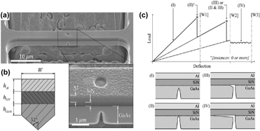
Another way to initiate stable interfacial delamination within a multilayer system is by the four-point bending of microbridges by Mead et al. [Reference Mead, Lu and Huang123]. Microscale prenotched bridges with clamped ends were machined into an Al/SiN/GaAs multilayer using FIB milling as shown in Fig. 15. A square flat-end indenter was used to induce bending of the bridge by two contact locations. Bridge failure occurred via substrate fracture at the prenotch, followed by crack deflection, and stable interfacial delamination of the SiN/GaAs interface. Substrate fracture and delamination were identified within the obtained load–displacement curves as a pop-in and region of linear load reduction, respectively.
(a) SEM of the clamped beam viewed at 45° tilt. Al, SiN, and GaAs components are labeled. (b) Indicative beam cross-section. (c) Indicative load–deflection curve with position labels (I–IV) to explain the changes to the beam during the loading [Reproduced with permission from Elsevier [Reference Mead, Lu and Huang123]].

Conclusion
A quick overview of in situ microfracture techniques for nanoscale metal–metal multilayers has been presented in this paper. By analyzing fracture in situ, we have the ability to observe and even quantify the behavior as the crack propagates along or across the multilayers. These techniques are only possible by advances in electron microscopy and in situ instrumentation tools highlighted by the examples. The challenges of analyzing the fracture in multilayers are explained with the hope that with further understanding and experimentation, a systematic approach can be identified. FIB fabrication remains to be the popular choice to create the structures for in situ testing due to the convenience of visually seeing the structure being made inside the SEM to our specifications despite concerns of ion implantation influencing the fracture results.
Four recent examples of in situ microfracture experimentation were highlighted in this review. The fracture upon tensile testing of film on a substrate technique involves the use of a standard technique known to material scientists followed by an in situ examination of the multilayered film fracture profile through FIB and SEM. Though the substrate may influence the result of the fracture, the ease of testing and available fracture toughness equations provides an easy solution for those who need an overall K IC value of the multilayered film of interest under tensile conditions.
The in situ microfracture clamped beam bending provides a controlled method to analyze the fracture of free-standing nanoscale metal–metal multilayered film across the layers. Two particular case studies were looked into using this technique—interface shear strength determination through clamped beam bending and influence of fabrication technique on the FCC/BCC interface role in fracture. Both case studies highlighted the influence of the multilayered interface and grain size and boundary in the fracture of these multilayers. However, more work needs to be done on the quantification of the fracture measurements obtained. Last but not least, the technique of delamination along the layers highlighted the need to measure the residual stresses of the individual layers before performing the fracture across the layers by the ion layer removal method. The directed notch cantilever beam method of the film on the silicon substrate allows for the crack to propagate from the notch to the interface of interest along the layers with the ease of calculation using the J-integral method.
It is obvious today that we have to evaluate the fracture behavior of materials at the length scales where they are used in applications, which is progressively getting miniaturized. Some of the challenges of in situ technique are the availability of high-resolution video imaging, the absence of true displacement control, accounting for plastic penetration of indenter and machine compliance among most in situ indenters. Some key scientific questions that need to be addressed for nanoscale metal–metal multilayers are as follows:
(1) How does one quantify the fracture behavior of heterogeneous material system such as multilayers at the nanoscale? Currently, a few assumptions are taken to approximately quantify this value due to the size of the structure, the electron microscopy (SEM versus TEM), and the employed mechanical technique, but a more detailed study is required into the quantification of crack propagation and eventual fracture toughness either analytically or through simulations.
(2) Is the continuum-based fracture mechanics criterion still valid for the dimensions of the microfracture beam structures? Can these techniques be used for even smaller structures like 2D nanomaterials or even graphene?
These direct observations and insights could lead to the enabling of the novel and extreme materials design. An example is the Cu/Nb metal/metal nanolayers with a possibility of tunable interface shear strength and thus unique fracture-delaying capacity. It requires a combined approach of simulations, in situ experimental measurements of real system interfaces, and finally quantification of the results to evaluate the fracture properties. It will also assist in the further and more in-depth exploration into the mechanical behavior of the nanoscale metal–metal multilayers and pursue on into other aspects such as elastic–plastic fracture mechanics (EPFM), dynamic testing, and fatigue and reliability studies. Some possible research areas to consider are in situ studies of metal–metal multilayered composites under high temperature, environmental conditions (i.e., humidity, moisture, or gas exposure) and phase changes at the nanoscale. With this understanding, nanoscale metal–metal multilayers can be further designed and even tuned for enhanced mechanical properties that could be useful for specific technological applications.
Acknowledgments
This work is also funded by the SUTD-MIT International Design Center (IDC), Singapore, under contract IDG31400102.