Introduction
Since 2000, the extraordinary versatility and the large potential for employing vertical free-standing semiconducting nanowires (NWs) as mesoscopic components in next-generation devices in the areas of electronics, photonics, and biochemical sensing have been demonstrated [Reference Duan, Huang, Cui, Wang and Lieber1, Reference Wang, Gudiksen, Duan, Cui and Lieber2, Reference Cui and Lieber3, Reference Thelander, Matensson, Björk, Ohlsson, Larsson, Wallenberg and Samuelson4, Reference Duan, Huang, Agarwal and Lieber5, Reference Zhang, Li, Liu, Han, Tang and Zhou6, Reference Offermans, Crego-Calama and Brongersma7, Reference Tian, Zheng, Kempa, Fang, Yu, Yu, Huang and Lieber8, Reference Wallentin, Anttu, Asoli, Huffman, Åberg, Magnusson, Siefer, Fuss-Kailuweit, Dimroth, Witzigmann, Xu, Samuelson, Deppert and Borgström9, Reference Han, Wang, Hou, Yip, Lin, Xiu, Fang, Yang, Shi, Dong, Hung and Ho10, Reference Hong, Yang, Lee, Ruoff, Kim and Fukui11, Reference Ren, Hu, Zhang, Zhu, Zhuang, Ma, Fan, Zhou, Liao, Duan and Pan12]. For example, practical ways for incorporating vertical surrounding-gate field-effect transistors (FET) based on vertical NWs into current integrated circuits based on CMOS technologies have been introduced [Reference Bao, Yakimets, Ryckaert, Ciofi, Baert, Veloso, Boemmels, Collaert, Roussel, Demuynck, Raghavan, Mercha, Tokei, Verkest, Thean and Wambacq13]. So far, the majority of the publications on NWs is based on NWs synthesized by the vapor–liquid–solid (VLS) method, a very popular bottom-up fabrication technique. The VLS method typically uses gold nanoparticles as catalysts. However, such conventional metal catalysts may lead to deterioration of the performance of NW devices mainly due to deep-level formation by incorporated metal impurities. In addition, the VLS-grown NWs are randomly distributed on a semiconducting substrate in most cases, which might hinder practical applications of NWs in devices in the future. We, on the other hand, have demonstrated the catalyst-free formation of vertical free-standing semiconducting NW arrays, e.g., GaAs, InGaAs, InP, InAs, GaAs/AlGaAs core–shell, and GaAs/GaAsP core–shell NWs, by selective-area growth, or selective-area metal–organic vapor-phase epitaxy (SA-MOVPE), using partially SiO2-masked {111}A and B substrates. The SA-MOVPE method yields a precise control of the size, aspect ratio, position, and density of NWs on various semiconducting substrate materials [Reference Sato, Kobayashi, Motohisa, Hara and Fukui14, Reference Tomioka, Motohisa, Hara and Fukui15]. Nanoelectronic devices such as vertical surrounding-gate FETs have been fabricated, and their performance has been demonstrated. Thus, our semiconducting NWs grown by SA-MOVPE possess a great potential for future device applications [Reference Tanaka, Tomioka, Hara, Motohisa, Sano and Fukui16, Reference Kobayashi, Kohashi, Hara and Motohisa17].
One of the most famous review papers, Ref. Reference Dasgupta, Sun, Liu, Brittman, Andrews, Lim, Gao, Yan and Yang18, dealing with semiconducting NW technologies was published by Yang’s group. It introduced an extremely wide variety of future applications of semiconducting NWs. Recent review articles on semiconducting NWs, on the other hand, mostly focus on an introduction to a specific topic related to a specific material property and/or device application. For example, progress in photovoltaic and energy applications [Reference Goktas, Wilson, Ghukasyan, Wagner, McNamee and LaPierre19, Reference Li, Tan, Jagadish and Fu20, Reference Mokkapati and Jagadish21], photonic and optical device applications [Reference Eaton, Fu, Wong, Ning and Yang22, Reference Holzman and Ivry23], electrical properties in the terahertz regime [Reference Joyce, Boland, Davies, Baig and Johnston24], biological and medical applications [Reference Wang, Lee, Koo and Kim25, Reference Doucey and Carrara26, Reference Li, Lu, Wang and Fan27], and electronic device characteristics [Reference Mikolajick, Heinzig, Trommer, Baldauf and Weber28, Reference Lind29] has been reported individually. The tendency of the latest review articles to focus on specific applications prominently indicates increasing expectations in now well-established semiconducting NW technologies to deliver results of industrial importance. However, only one of these review articles discusses the electrical spin injection and transport in semiconducting NWs [Reference Tang and Wang30]. Thus, the attractive perspective of semiconducting NW devices in the context of magneto-nanoelectronic or nanospintronic device applications has, to the best of our knowledge, not been reviewed yet. Activities to achieve diluted magnetic semiconductor (DMS) layers [Reference Gould, Pappert, Schmidt and Molenkamp31] and the heteroepitaxy of ferromagnetic layers and III–V compound semiconductors (FM III–V hybrids) have recently attracted great attention in semiconductor nanospintronics research owing to possible additional functionalities that may be added to current semiconducting devices and integrated circuits. Among these approaches, granular hybrid structures, in which ferromagnetic nanoclusters (NCs) are embedded into semiconductor layers, are one of the most attractive material candidates for future nanospintronic devices due to their huge magnetoresistance (MR) effects [Reference Elm, Klar, Ito and Hara32, Reference Michel, Elm, Goldlücke, Baranovskii, Thomas, Heimbrodt and Klar33, Reference Wellmann, Garcia, Fend and Petroff34, Reference Elm, Michel, Stehr, Hofmann, Klar, Ito, Hara and Krug von Nidda35, Reference Hai, Ohya, Tanaka, Barnes and Maekawa36] and a comparatively long spin-relaxation time [Reference Hai, Ohya and Tanaka37, Reference Tanaka, Ohya and Hai38]. Devices of these materials have been fabricated on semiconducting substrates mostly by low-temperature molecular beam epitaxy in combination with conventional top-down fabrication techniques. Various kinds of NWs based on FM III–V hybrids or DMSs [Reference Radovanovic, Barrelet, Gradečak, Qian and Lieber39] have recently been synthesized to produce NW spintronic devices using several techniques based on the conventional VLS method as the bottom-up fabrication approach, e.g., GaMnAs NWs [Reference Kim, Cho, Kong, Kim, Chung, Park, Kim, Yoon, Jung, Jo, Kim and Ahn40, Reference Borschel, Messing, Borgström, Paschoal, Wallentin, Kumar, Mergenthaler, Deppert, Canali, Pettersson, Samuelson and Ronning41], GaAs/GaMnAs core–shell NWs [Reference Rudolph, Soda, Kiessling, Wojtowicz, Schuh, Wegscheider, Zweck, Back and Reiger42, Reference Yu, Wang, Pan, Zhao, Misuraca, von Molnár and Xiong43], MnAs nanoparticles on InAs [Reference Ramlan, May, Zheng, Allen, Wessels and Lauhon44] and GaAs [Reference Wolff, Görlitz, Nielsch, Messing and Deppert45] NWs, GaAs/MnAs core–shell NWs [Reference Hilse, Takagaki, Herfort, Ramsteiner, Herrmann, Breuer, Geelhaar and Riechert46, Reference Liang, Wang, Paul, Cooley, Rench, Dellas, Mohney, Engel-Herbert and Samarth47], GaN-related DMS NWs [Reference Radovanovic, Barrelet, Gradečak, Qian and Lieber39, Reference Choi, Seong, Chang, Lee, Park, Kim, Lee, He, Kuykendall and Yang48, Reference Seong, Kim, Kim, Lee, Kim, Kim, Park and Choi49], heterojunction NWs between MnGe alloys and Ge [Reference Lensch-Falk, Hemesath and Lauhon50, Reference Tang, Wang, Hung, Jiang, Chang, He, Liu, Yang, Tuan, Chen and Wang51] and between MnSi alloys and Si [Reference Lin, Chen, Shailos and Huang52], and vertical multiple-segment AuGe/Ge NWs [Reference Li, Meng, Qin, Xu, Chu, Zhu, Kong and Li53]. However, it is also crucial to recognize, avoid, and overcome possible problems arising in the growth process which may limit the performance of current and future nanoelectronic and photonic NW devices. One challenge, in particular when using conventional VLS methods in the growth of NWs, is to avoid metal impurities in the NW material originating from the metal catalysts employed. Therefore, we have developed a hybridization technique to grow ferromagnetic MnAs NCs [Reference Hara, Kawamura, Iguchi, Motohisa and Fukui54] on vertical free-standing semiconducting NW templates grown by our catalyst-free SA-MOVPE technique [Reference Sato, Kobayashi, Motohisa, Hara and Fukui14, Reference Tomioka, Motohisa, Hara and Fukui15] in the research field of semiconductor nanospintronics, and reported on the formation and characterizations of MnAs NC/GaAs hybrid NWs [Reference Yatago, Iguchi, Sakita and Hara55, Reference Hara, Sakita and Yatago56]. The SA-MOVPE technique allows us to directly synthesize single-crystal ferromagnetic MnAs NCs on a semiconducting substrate. We also demonstrated that the NCs can be used as promising building blocks for fabricating future nanospintronic devices as they exhibit large angle-dependent MR effects [Reference Elm, Klar, Ito, Hara and Krug von Nidda57, Reference Fischer, Elm, Sakita, Hara and Klar58]. However, it still remains challenging to form vertical heterojunction NWs between ferromagnetic MnAs and semiconducting layers. Such vertical heterojunctions would enable the injection of spin-polarized carriers and currents into semiconducting NW channels [Reference Zwanenburg, van der Mast, Heersche, Kouwenhoven and Bakkers59]. However, it remains challenging to control the crystal orientations of the MnAs NCs on a 〈111〉B-oriented GaAs NW template [Reference Yatago, Iguchi, Sakita and Hara55, Reference Hara, Sakita and Yatago56] and to obtain atomically abrupt heterointerfaces between MnAs and GaAs even when using our hybridization techniques. It is likely that the difficulties in forming vertical heterojunction NWs are mainly due to the rather stable crystal facet of the c-plane, i.e., the {0001}-oriented surface, of hexagonal NiAs-type MnAs NCs grown by SA-MOVPE [Reference Yatago, Iguchi, Sakita and Hara55]. We believe that the combination of a magnetic tunnel junction electrode (e.g., CoFeB/MgO [Reference Inokuchi, Marukame, Ishikawa, Sugiyama and Saito60] and CoFe/MgO [Reference Jiang, Wang, Shelby, Macfarlane, Bank, Harris and Parkin61]) and vertical ferromagnetic/semiconducting heterojunction NWs with atomically abrupt heterointerfaces [Reference Tang, Wang, Hung, Jiang, Chang, He, Liu, Yang, Tuan, Chen and Wang51] could overcome major obstacles of conductance mismatch and poor controllability of heterointerface formation in current spin MOSFETs [Reference Sugahara and Nitta62]. In addition, the {111}B-oriented semiconducting NW channels may also have a great advantage for enhancing spin lifetime in the channels of spin MOSFETs [Reference Biermann, Hernandez-Minguez, Hey and Santos63].
Thus, in this paper, we introduce our recent technological developments for the synthesis of high-quality vertical ferromagnetic MnAs NC/semiconducting InAs heterojunction NWs with atomically abrupt heterointerfaces on semiconducting substrates utilizing the so-called endotaxy of MnAs NCs after the selective-area growth, i.e., SA-MOVPE, of host InAs NW templates and by adjusting the synthesis conditions [Reference Kodaira, Hara, Kabamoto and Fujimagari64, Reference Kabamoto, Kodaira and Hara65, Reference Kodaira, Kabamoto and Hara66, Reference Kodaira, Horiguchi and Hara67]. After the structural and magnetic characterizations by transmission electron microscopy and magnetic force microscopy (TEM and MFM, respectively), we show some preliminary results of the transport properties of InAs host NWs and MnAs/InAs heterojunction NWs. The temperature dependence of the resistance and the magnetotransport properties of NWs were investigated. We believe that our vertical ferromagnetic MnAs NC/semiconducting InAs heterojunction NWs in the current work are definitely exhibiting new possibilities and versatility for creating novel magneto-nanoelectronic or nanospintronic devices using vertical free-standing semiconducting NWs, e.g., spin-NW-MOSFETs, spin-NW-light-emitting diode arrays, and NW-array-terahertz-wave emitters, as was reported and discussed in our review paper [Reference Elm and Hara68].
Results and discussion
Selective-area growth and endotaxy
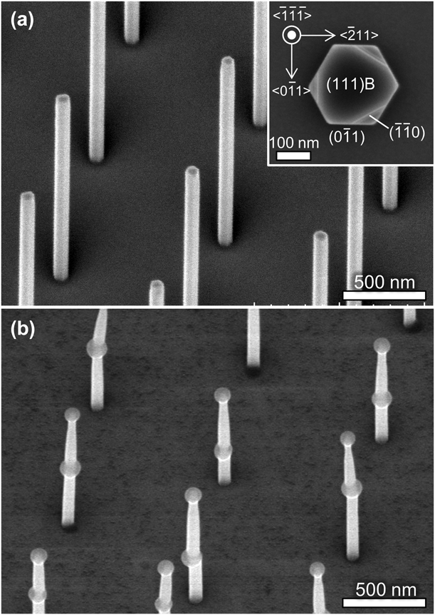
At first, a template structure of InAs NW arrays was grown by SA-MOVPE to fabricate vertical ferromagnetic MnAs NC/semiconducting InAs heterojunction NWs. Figure 1(a) shows a typical bird’s-eye view obtained by secondary electron imaging with scanning electron microscopy (SEM) of the template structure of InAs NW arrays before the growth of MnAs NCs. Prior to the growth, initial circular openings with diameters, d 0, of 110–140 nm and a period, or pitch, a, of 1.0 μm were prepared in the SiO2 thin films. The diameter of the resulting InAs NWs shown in Fig. 1(a) is estimated to be approximately 150 nm and their height is about 1.5 μm. For initial circular openings with d 0 between 80 and 90 nm, typically InAs NWs with a diameter of approximately 120 nm are grown. The inset in Fig. 1(a) is a highly magnified top view of one of the InAs NWs. The InAs NWs reveal a hexagonal prismatic shape surrounded by six  $\left\{ {0\bar{1}1} \right\}$ crystal facets and grow in the 〈111〉B direction on the GaAs(111)B substrates. The top of the NWs reveals that flat {111}B crystal facets surrounded by tilted
 $\left\{ {\bar{1}\bar{1}0} \right\}$ ones are formed during the growth. Figure 1(b) shows typical ferromagnetic MnAs NC/semiconducting InAs hybrid NWs grown at 580 °C for 1 min. The NCs are formed on the top {111}B crystal facets of the InAs NWs, and also some additional NCs are grown around the middle parts of the NWs. We utilized the phenomenon of the “endotaxy” of MnAs in InAs for the growth of MnAs NCs after the InAs NW growth [Reference Bonev69]. Endotaxy is associated with a diffusion process that leads to a redistribution of substances, i.e., MnAs NCs in the host crystals, InAs NWs in the current work, and the formation of new stable phases, as introduced in Ref. Reference Bonev69. This is the key technique for forming ferromagnetic MnAs NCs “inside” semiconducting NWs grown by SA-MOVPE [Reference Yatago, Iguchi, Sakita and Hara55, Reference Hara, Sakita and Yatago56, Reference Hara, Fujimagari, Sakita and Yatago70]. The endotaxial nanoclustering of magnetic materials in semiconducting thin films has also been observed in other material systems, such as MnSb:GaSb [Reference Braun, Trampert, Kaganaer, Jenichen, Satapathy and Ploog71] and MnP:GaP [Reference Nateghi, Ménard and Masut72] thin films.
Bird’s-eye views of secondary electron microscope images of a typical (a) host InAs NW array template before the synthesis of MnAs NCs and (b) MnAs/InAs heterojunction NWs. The inset of (a) is a top view of the secondary electron microscope image of the crystal facets typically formed on top of host InAs NWs. Reprinted with permission from Ref. Reference Kodaira, Hara, Kabamoto and Fujimagari64 [Copyright (2016), the Japan Society of Applied Physics].

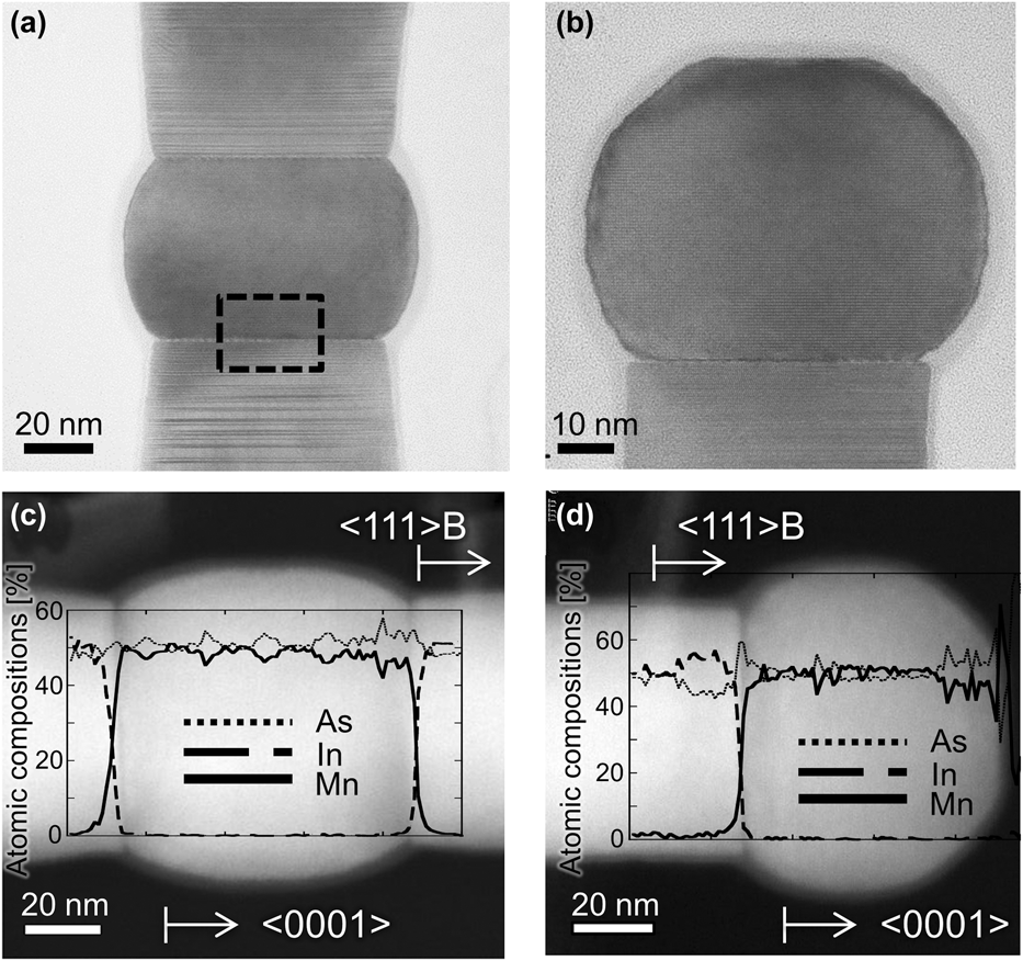
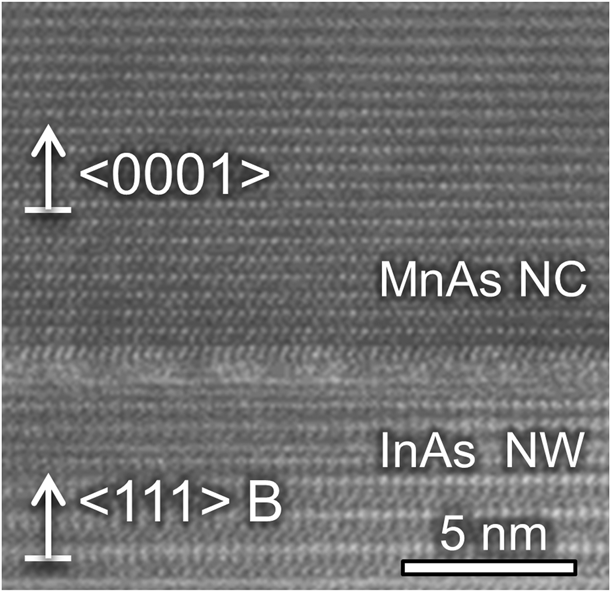
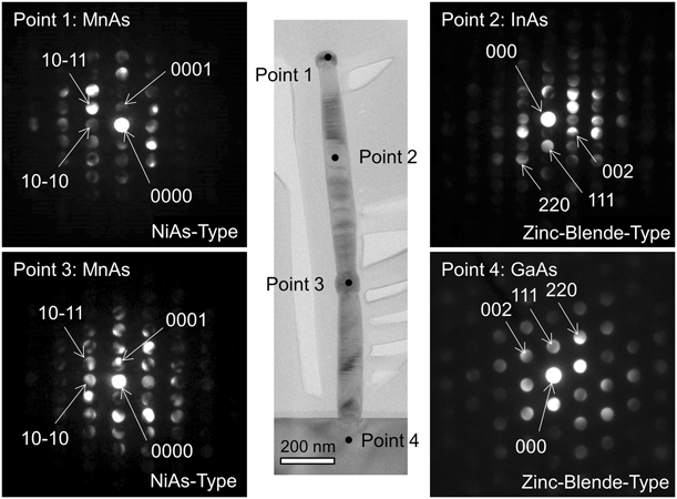
Structural characterization was conducted by TEM for comparable hybrid NWs to carefully investigate the structural characteristics of the ferromagnetic MnAs NC/semiconducting InAs hybrid NWs shown in Fig. 1(b). Figures 2(a) and 2(b) show highly magnified cross-sectional bright-field TEM images of the MnAs NCs that were formed in the middle and on the top {111}B crystal facets of the host InAs NWs, respectively. The width and height of the NC in Fig. 2(a) were estimated to be approximately 85 and 55 nm, respectively, and those in Fig. 2(b) were estimated to be approximately 72 and 54 nm, respectively. TEM measurements confirm that rotational twin defects are randomly formed in the InAs NWs, and that no dislocations or other defects, on the other hand, can be observed in the MnAs NCs. The characterization results of energy-dispersive X-ray (EDX) spectroscopy of the corresponding MnAs NCs are shown in Figs. 2(c) and 2(d), respectively. The atomic compositions of the NCs and NWs in terms of three elements, i.e., arsenic, indium, and manganese, were estimated from the line profiles obtained by EDX spectroscopy. This way we precisely determined the solid compositions of the NCs and NWs and eliminated possible external contamination by chemicals (or atoms), such as carbon, oxygen, and silicon, which were possibly introduced during the sample preparation processes or originated from the materials of the sample holders used for the TEM observations. The solid compositions (atomic compositions in %) of arsenic, indium, and manganese elements are found to correspond to approximately 52, 1.0, and 47%, respectively, in the regions of the NC positioned in the middle of the host InAs NWs, as shown in Fig. 2(c). The MnAs NC formed on the top {111}B crystal facets of the host InAs NWs has similar solid compositions of approximately 51, 0, and 49% of arsenic, indium, and manganese elements, respectively, as shown in Fig. 2(d). Figure 3 shows a lattice image of the interface between the NW and the NC which was formed in the middle of the NW. As shown in Fig. 3, atomically abrupt heterointerfaces are formed between the MnAs NC and InAs NW. It appears that a small number of the observed MnAs NCs investigated are possibly rotated along the c-axes parallel to the 〈111〉B directions of the host InAs NWs according to additional cross-sectional lattice images of the NCs (not shown here). Similar results in terms of the heterointerfaces were obtained for the NCs formed on the top {111}B crystal facets of the NWs. The results of the structural characterization show that vertical ferromagnetic MnAs NC/semiconducting InAs heterojunction NWs with atomically abrupt heterointerfaces were successfully grown by utilizing the endotaxy of MnAs NCs at a growth temperature, T g, of 580 °C. In addition to the cross-sectional lattice images by TEM, the electron-beam diffraction (ED) patterns from the MnAs NC, the host InAs NW, and the GaAs substrate were measured, as shown in Fig. 4. The ED patterns reveal that the MnAs NCs exhibit a hexagonal NiAs-type crystal structure, which is confirmed by the ED patterns of points 1 and 3 in Fig. 4. The host InAs NW and the GaAs substrate, on the other hand, have a zinc-blende-type crystal structure, as shown in the ED patterns of points 2 and 4 in Fig. 4, respectively. The c-axis, i.e., the 〈0001〉 direction, of the NiAs-type MnAs NCs is approximately parallel to the 〈111〉B direction of the host zinc-blende-type InAs NWs. The possible growth mechanism and the formation control of MnAs NCs in the host InAs NWs as the result of endotaxy are discussed in detail in our previous studies [Reference Kodaira, Hara, Kabamoto and Fujimagari64, Reference Kodaira, Kabamoto and Hara66].
Cross-sectional TEM images of ferromagnetic MnAs NC formed (a) in the middle and (b) on the top {111}B crystal facet of semiconducting InAs NWs. MnAs NCs were grown at 580 °C for 1 min. Cross-sectional TEM images with corresponding line profile obtained by energy-dispersive X-ray spectroscopy for (c) middle and (d) top of NW. The percentages of arsenic, indium, and manganese atoms were estimated by eliminating possible external contamination by chemicals or atoms, such as carbon, oxygen, and silicon, which were possibly introduced during the sample preparation processes and from materials of the sample holders used for TEM observations. Reprinted with permission from Ref. Reference Kodaira, Hara, Kabamoto and Fujimagari64 [Copyright (2016), the Japan Society of Applied Physics].

Lattice image of an atomically abrupt heterointerface between InAs and MnAs that is formed in the middle of a MnAs/InAs heterojunction NW. The observed area is indicated by a black dashed line in Fig. 2(a). Reprinted with permission from Ref. Reference Kodaira, Hara, Kabamoto and Fujimagari64 [Copyright (2016), the Japan Society of Applied Physics].

Cross-sectional transmission electron microscope image and electron diffraction patterns of vertical ferromagnetic MnAs nanocluster (NC)/semiconducting InAs heterojunction NWs on GaAs(111)B substrates: Points 1 and 3 for MnAs NCs, Point 2 for InAs NW, and Point 4 for GaAs(111)B substrate. The MnAs NCs were grown at 580 °C for 1 min. Reprinted with permission from Ref. Reference Kodaira, Hara, Kabamoto and Fujimagari64 [Copyright (2016), the Japan Society of Applied Physics].

Magnetization
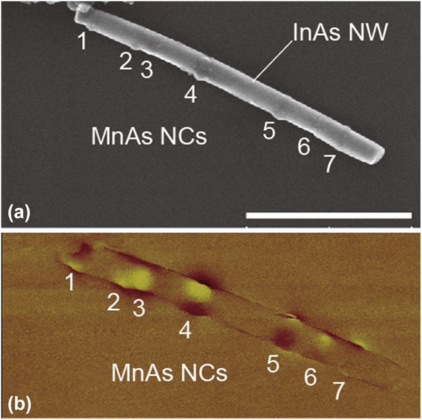
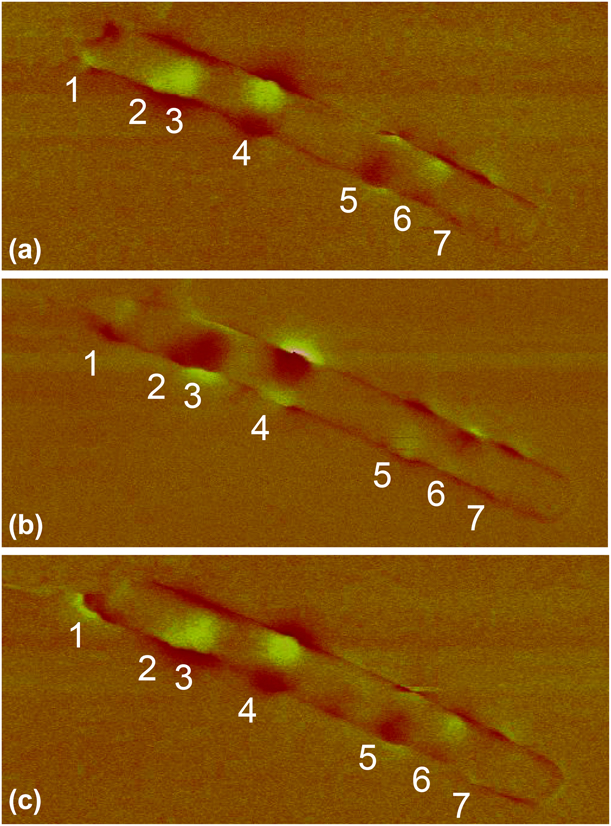
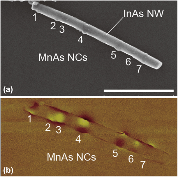
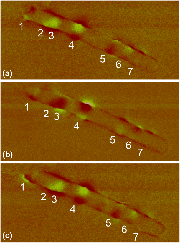
In this section, we introduce typical magnetization characterization results of the MnAs/InAs heterojunction NWs by MFM performed at room temperature. The sample used in the current work is the same one used in our previous study, Ref. Reference Kabamoto, Kodaira and Hara65. Figure 5 shows the secondary electron and MFM images of a typical MnAs/InAs heterojunction NW. We identify seven MnAs NCs in the host InAs NW, which are labeled in the view graphs as #1 to #7 from the left to right, using a combined characterization by SEM and MFM. Since the MFM image in Fig. 5(b) was obtained without applying an external magnetic field, B, before and during the MFM observation, the measurements clearly confirm the presence of spontaneous magnetization, i.e., a ferromagnetic behavior, of the MnAs NCs at room temperature. Subsequently, MFM measurements with different orientations of the tip magnetization were performed for the same MnAs/InAs heterojunction NW. The corresponding results are shown in Fig. 6. The directions of the MFM tip magnetization are downward and upward in Figs. 6(a) and 6(b), respectively. Prior to the MFM measurements shown in Figs. 6(a) and 6(b), a magnetic field of B = 500 Gauss was applied in the upward direction, perpendicular to the substrate. In the corresponding MFM images, the dark and bright contrasts correspond to attractive and repulsive forces respectively, which are detected by the magnetized MFM tips from the stray magnetic fields of the NCs. Therefore, the measurements clearly confirm that the magnetizations of the NCs affect the MFM tip. Figure 6(c), finally, shows the dependence of NC magnetization on an applied magnetic field, B, of the same MnAs/InAs heterojunction NW characterized in Figs. 5, 6(a), and 6(b). The MFM image in Fig. 6(c) was obtained by increasing the applied B to 2,000 Gauss. B was applied in the upward direction perpendicular to the substrate. The magnetization direction of the MFM tip used in the observations was downward, which was the same orientation as that employed in the measurements shown in Figs. 5(b) and 6(a). For both the applied B fields of 500 and 2,000 Gauss, no marked differences in the dark and bright contrasts at the NCs are observed (in addition, neither for B of 3,500 Gauss, not shown here). In other words, the dark–bright contrast series observed for NCs, #1 to #7, confirm a magnetization alignment, i.e., a magnetic easy axis, perpendicular to the 〈111〉B direction of the NW. As shown in the TEM observations (Figs. 2–4), the c-axis, which is the magnetic hard axis of the hexagonal NiAs-type MnAs NCs, is parallel to the 〈111〉B direction of the zinc-blende-type InAs NWs. This means that the a-axes, which are the magnetic easy axes of the NCs, are oriented perpendicular to the 〈111〉B direction of the NWs in agreement with our MFM observations.
(a) Secondary electron microscope image of a typical MnAs/InAs heterojunction NW. White scale bar represents 1 μm. (b) Magnetic force microscope (MFM) image of the same MnAs/InAs heterojunction NW shown in (a). At room temperature, the NW clearly shows spontaneous magnetization only at positions #1 to #7, where we observe MnAs NCs, without any application of an external magnetic field. The magnetization direction of the MFM tip used in the MFM observation in (b) is downward. The NW characterized in the current work is the same one characterized by backscattered electron imaging in our previous study, Ref. Reference Kabamoto, Kodaira and Hara65.
MFM images for varying tip magnetization directions of the same MnAs/InAs heterojunction NW characterized in Fig. 5. The magnetization directions of the MFM tip are (a) downward and (b) upward. Applied magnetic field dependence of the magnetization direction for the same MnAs/InAs heterojunction NW was characterized. Prior to the investigations, an external magnetic field, B, of 500 Gauss was applied for (a) and (b), and B of 2,000 Gauss was applied for (c). The applied B direction was upward, perpendicular to the substrate in all the cases. For (c), the magnetization direction of the MFM tip used in the observation is downward, which is the same as the case of (a).
Bulk MnAs shows a first-order structural phase transition between the paramagnetic orthorhombic β-phase (β-MnAs, MnP-type) and the ferromagnetic hexagonal α-phase (α-MnAs, NiAs-type) in the vicinity of room temperature. From our TEM characterization in the previous section, we conclude that the MnAs NCs in the MnAs/InAs heterojunction NWs are α-MnAs with a NiAs-type crystallographic structure. A detailed discussion of the MnAs crystal phase of comparable samples has been reported elsewhere [Reference Kodaira, Horiguchi and Hara67]. We have not determined the Curie temperature, T c, of the MnAs NCs in the InAs NWs in the current work. However, in our previous studies, measurements of the hysteresis curves [Reference Hara and Fukui73] and the magnetization [Reference Elm, Michel, Stehr, Hofmann, Klar, Ito, Hara and Krug von Nidda35] reveal an increased T c of 340 K for comparable samples with NiAs-type MnAs NCs on InGaAs(111)B layers. For different types of the samples with MnAs NCs formed in Mn-incorporated InGaAs(001) layers, we observed a decrease in T c from 320 to 290 K, probably caused by a change in the solid composition of the NCs from MnAs to MnP, due to the existence of undoped InP capping layers on the top of InGaAs(001) layers with MnAs NCs [Reference Hara, Lampalzer, Torunski, Volz, Treutmann and Stolz74]. Some researchers have also reported on MnAs NCs with a single magnetic domain, which were epitaxially grown on GaAs NWs. From measurements of the hysteresis curve of the MnAs NCs, they estimated a T c of 313 K for such MnAs NCs on GaAs NWs [Reference Hubmann, Bauer, Körner, Furthmeier, Buchner, Bayreuther, Dirnberger, Schuh, Back, Zweck, Reiger and Bougeard75]. Thus, the T c of the MnAs NCs in InAs NWs in the current work can be expected to be larger than 320 K.
Transport properties
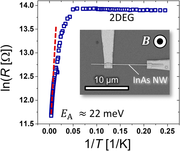
To investigate the influence of the MnAs NCs on the transport properties of the MnAs NC/semiconducting InAs heterojunction NWs, we performed first measurements of the temperature dependence of the resistance and magnetotransport measurements. For comparison, transport measurements were also performed for the InAs host NW without MnAs NCs, i.e., grown by the same SA-MOVPE process without a subsequent endotaxy step. Figure 7 shows the temperature-dependent resistance of a single InAs NW in an Arrhenius representation. At high temperatures, the NW exhibits a thermally activated transport behavior with an exponential increase in resistance with decreasing temperature following Arrhenius’ law:
 $$R\left( T \right) = {R_0}\;{\rm{exp}}\left( {{{{E_{\rm{A}}}} \over {{k_{\rm{B}}}T}}} \right)\quad .$$
Temperature dependence of a host InAs NW showing an activated transport behavior at higher temperatures with an activation energy of about 22 meV. At low temperatures, the resistance slightly decreases with decreasing temperature, indicating the formation of a two-dimensional electron gas (2DEG). The dashed line corresponds to the linear fit of the high-temperature region.
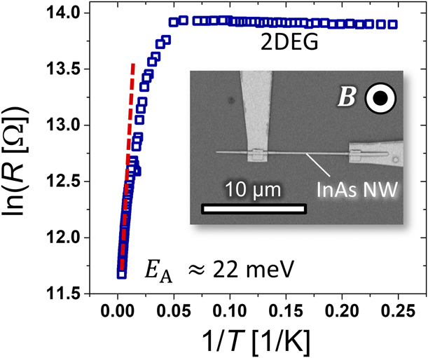
Using a linear fit, the activation energy E A in the temperature range between 120 and 280 K was determined to be around 22 meV. Comparable activation energies ranging between 10 and 25 meV were also reported for InAs NWs grown by low-pressure MOVPE or InAs thin films, and are attributed to structural defects, i.e., twin boundaries, stacking faults [Reference Wirths, Weis, Winden, Sladek, Volk, Alagha, Weirich, von der Ahe, Hardtdegen, Lüth, Demarina, Grützmacher and Schäpers76] between wurtzite and zinc blende, or arsenic vacancies [Reference Voronina, Lagunova, Moiseev, Rozov, Sipovskaya, Stepanov, Sherstnev and Yakovlev77]. At temperatures below T = 25 K, the resistance saturates and even slightly decreases with decreasing temperature. This behavior indicates the formation of a two-dimensional electron gas (2DEG) at the NW surface, which arises due to pinning of the Fermi energy at surface states above the conduction band edge [Reference Blömers, Lepsa, Luysberg, Grützmacher, Lüth and Schäpers78, Reference Estévez Hernández, Akabori, Sladek, Volk, Alagha, Hardtdegen, Pala, Demarina, Grützmacher and Schäpers79, Reference Olsson, Andersson, Håkansson, Kanski, Ilver and Karlsson80, Reference Noguchi, Hirakawa and Ikoma81].
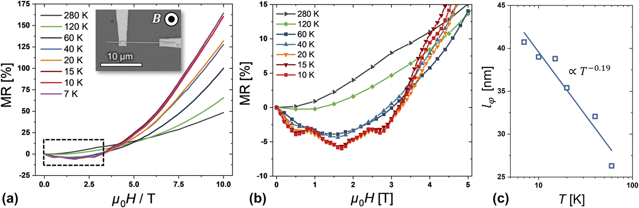
The magnetotransport properties of the InAs NW were investigated for a magnetic field, B, oriented perpendicular to the NW axis. As shown in Fig. 8(a), a strong positive MR effect is observed in the whole temperature range investigated. At 280 K, the NW exhibits a MR effect of about 50%, which increases with decreasing temperature up to 165% at 7 K. The large positive MR effect is often observed in thin InAs layers and arises from the formation of the 2DEG surface accumulation layer [Reference Sun, Soh and Kosel82, Reference Wieder83]. The charge-accumulation layer at the surface forms a second alternative transport channel for the charge carriers in addition to the transport path through the bulk. The positive MR observed under these circumstances can be described well by the two-band model [Reference Sun, Soh and Kosel82, Reference Wieder83, Reference McCarthy84, Reference Tsuji and Okamoto85] introduced by Nedoluha and Koch [Reference Nedoluha and Koch86].
(a) MR of the host InAs NW at different temperatures and for a magnetic field applied perpendicular to the NW axis. (b) Negative MR effect and universal conduction fluctuations at low temperatures for the regions indicated by a black dashed rectangle. (c) Temperature dependence of the phase coherence length l φ determined from the analysis of the WL effect.
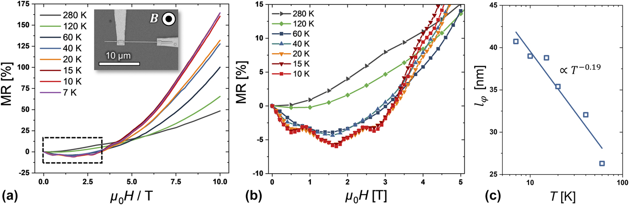
As shown in Fig. 8(b), at low temperatures also electron interference phenomena contribute to the MR of the InAs NW investigated, i.e., a negative MR contribution due to a weak localization (WL) effect [Reference Bergmann87] and universal conductance fluctuations (UCFs) [Reference Lee, Stone and Fukuyama88, Reference Washburn and Webb89] are observed for temperatures below 60 K. Such interference effects typically occur in mesoscopic samples, e.g., NWs [Reference Blömers, Lepsa, Luysberg, Grützmacher, Lüth and Schäpers78, Reference Estévez Hernández, Akabori, Sladek, Volk, Alagha, Hardtdegen, Pala, Demarina, Grützmacher and Schäpers79, Reference Elm, Uredat, Binder, Ostheim, Schäfer, Hille, Müßener, Schörmann, Eickhoff and Klar90, Reference Yang, Wang, Hsu and Lin91, Reference Uredat, Hille, Schoermann, Klar, Eickhoff and Elm92], whose dimensions are smaller or comparable to the so-called electron phase-coherence length l φ, which is the characteristic length over which the electron phase is maintained [Reference Lin and Bird93]. The phase coherence length can be determined from the WL effect, the magnitude of the fluctuations rms (ΔG), or the so-called correlation field B C [Reference Elm, Uredat, Binder, Ostheim, Schäfer, Hille, Müßener, Schörmann, Eickhoff and Klar90, Reference Uredat, Hille, Schoermann, Klar, Eickhoff and Elm92, Reference Beenakker, van Houten, Ehrenreich and Turnbull94]. For the InAs NW, we analyzed only the WL effect in small magnetic fields up to 0.5 T. For higher magnetic fields, the positive MR contribution dominates the overall MR behavior, making it impossible to determine the phase coherence length from the universal conductance fluctuations. For quasi-one-dimensional transport in the weakly disordered regime, the phase coherence length can be determined from the WL magnetoconductance in the low magnetic field limit, which is given by [Reference Hansen, Björk, Fasth, Thelander and Samuelson95, Reference Roulleau, Choi, Riedi, Heinzel, Shorubalko, Ihn and Ensslin96]:
 $$\eqalign{{\rm{\Delta }}G\left( B \right) = \cr- {2 \over L}{{{{\rm{e}}^2}} \over h}\left[ {{3 \over 2}{{\left( {{1 \over {l_\varphi ^2}} + {4 \over {3l_{{\rm{SO}}}^2}} + {1 \over {D{\tau _{\rm{B}}}}}} \right)}^{ - {1 \over 2}}} - {1 \over 2}{{\left( {{1 \over {l_\varphi ^2}} + {1 \over {D{{\rm{\tau }}_{\rm{B}}}}}} \right)}^{ - {1 \over 2}}}} \right]\quad .$$
The relaxation time τB is given by [Reference Hansen, Björk, Fasth, Thelander and Samuelson95]
 $${\tau _{\rm{B}}} = {{3l_{\rm{B}}^4} \over {{w^2}D}}\quad ,$$
where  ${l_{\rm{B}}} = \sqrt {{\hbar / {{\rm{e}}B}}}$ denotes the magnetic length; D denotes the diffusion coefficient; w = 110 nm and L = 7800 nm are the NW diameter and its length, respectively; and l SO is the spin–orbit interaction length. Depending on the ratio between l φ and l SO, a change from WL to weak anti-localization (WAL) can occur [Reference Hansen, Björk, Fasth, Thelander and Samuelson95, Reference Roulleau, Choi, Riedi, Heinzel, Shorubalko, Ihn and Ensslin96, Reference Dhara, Solanki, Singh, Narayanan, Chaudhari, Gokhale, Bhattacharya and Deshmukh97]; i.e., for l φ < l SO WL is observed, while for l φ > l SO, strong spin–orbit coupling results in a WAL, i.e., a positive correction of the conductance with increasing magnetic field, are observed [Reference Dhara, Solanki, Singh, Narayanan, Chaudhari, Gokhale, Bhattacharya and Deshmukh97, Reference Wang, Guo, Kang, Pan, Li, Fan, Zhao and Xu98]. We conclude that spin–orbit coupling is negligible because in our InAs NW, only a WL effect is observed and, thus, l φ ≪ l SO. Equation (2) is then simplified to [Reference Uredat, Hille, Schoermann, Klar, Eickhoff and Elm92, Reference Dhara, Solanki, Singh, Narayanan, Chaudhari, Gokhale, Bhattacharya and Deshmukh97]
 $$\Delta G\left( B \right) = - {2 \over L}{{{{\rm{e}}^2}} \over h}{\left( {{1 \over {l_\varphi ^2}} + {{{e^2}{B^2}{w^2}} \over {3\hbar }}} \right)^{ - {1 \over 2}}}\quad .$$
Figure 8(c) shows the l φ values determined by fitting Eq. (4) to the WL effect at the low magnetic field (B ≤ 0.5 T) as a function of temperature, revealing a decrease of l φ with increasing temperature following a T −0.19 dependence. According to theory, a temperature dependence of l φ ∝ T −1/3 is expected as quasi-elastic electron–electron scattering (Nyquist dephasing) is the dominant phase-breaking mechanism in one-dimensional nanostructures at low temperatures [Reference Lin and Bird93, Reference Altshuler, Aronov and Khmelnitsky99]. However, a slightly smaller absolute value of the exponent, such as 0.19 in our case instead of the theoretically predicted 0.33, is often observed in semiconducting NWs [Reference Elm, Uredat, Binder, Ostheim, Schäfer, Hille, Müßener, Schörmann, Eickhoff and Klar90, Reference Uredat, Hille, Schoermann, Klar, Eickhoff and Elm92, Reference Alagha, Estévez Hernández, Blömers, Stoica, Calarco and Schäpers100, Reference Blömers, Schäpers, Richter, Calarco, Lüth and Marso101]. Also, a phase coherence length of about 40 nm at T = 7 K is in good agreement with other values reported in the literature at low gate voltages and comparable temperatures [Reference Liang, Sakr and Gao102, Reference Liang and Gao103].
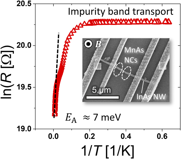
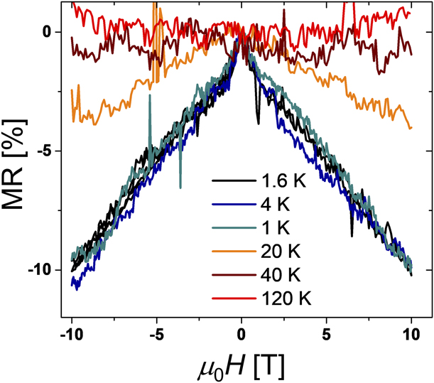
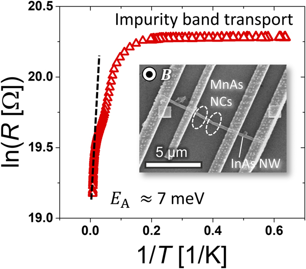
The temperature dependence of the resistance of a MnAs/InAs heterojunction NW including two MnAs NCs is shown in Fig. 9. As for the InAs NW, the MnAs/InAs heterojunction NW shows a thermally activated transport behavior at high temperatures between 50 and 280 K. However, the activation energy determined in this temperature range is drastically reduced to approximately 7 meV compared to 22 meV in the InAs NWs. This change in the activation energy is attributed to a high Mn doping of the semiconducting NW during the endotaxy of the MnAs NCs. In InAs, Mn is incorporated on the In lattice site and, thus, acts as an acceptor dopant with an activation energy for the isolated impurity of about 20–30 meV above the valence band maximum [Reference Okabayashi, Mizokawa, Sarma, Fujimori, Slupinski, Oiwa and Munekata104, Reference Shen, Zhao, Bai, Yu, Liu, Xie, Dong, Yang, Yang and Wang105, Reference Chiu, Blattner, May and Wessels106]. With increasing doping concentration, a broad impurity band is formed, reducing the activation energy for activated transport in the high temperature region. At temperatures below 50 K, transport takes places in the impurity band, resulting in a nearly metallic transport with an activation energy of about 3 µeV. A comparable behavior is also found for highly doped GaN:Ge [Reference Elm, Uredat, Binder, Ostheim, Schäfer, Hille, Müßener, Schörmann, Eickhoff and Klar90] NWs or GaAs:Mn NWs [Reference Borschel, Messing, Borgström, Paschoal, Wallentin, Kumar, Mergenthaler, Deppert, Canali, Pettersson, Samuelson and Ronning41]. The strong influence of the incorporation of Mn into the NWs is also found in the MR behavior of the heterojunction NW shown in Fig. 10. For temperatures below 40 K, the NW exhibits a large linear negative MR, and even at higher temperatures, the large positive MR found in the case of the InAs NW completely vanishes. A negative MR effect is often observed in Mn-doped InAs [Reference Iye, Oiwa, Endo, Katsumoto, Matsukura, Shen, Ohno and Munekata107, Reference Ohno, Munekata, Penney, von Molnár and Chang108] or GaAs semiconductors [Reference Elm and Hara68, Reference Michel, Baranovskii, Thomas, Heimbrodt, Elm, Klar, Goldlücke, Wurstbauer, Reinwald and Wegscheider109, Reference Ohno110], which typically follows a Brillouin-like behavior. This negative MR effect is explained either by an alignment of the localized magnetic moments of the Mn atoms in the external field, which reduces spin-dependent scattering and thus results in a decreasing resistance [Reference Iye, Oiwa, Endo, Katsumoto, Matsukura, Shen, Ohno and Munekata107, Reference Edmonds, Campion, Wang, Neumann, Gallagher, Foxon and Main111, Reference May, Blattner and Wessels112], or by a magnetic field splitting of the valence bands due to p–d exchange interaction (giant Zeeman effect). In the latter case, the corresponding valence band is shifted toward the energetic position of the acceptor level, leading to an increase in the carrier concentration in the current-carrying band and, therefore, to a negative MR effect [Reference Michel, Baranovskii, Thomas, Heimbrodt, Elm, Klar, Goldlücke, Wurstbauer, Reinwald and Wegscheider109, Reference Michel, Klar, Baranovskii and Thomas113]. However, the Brillouin-like decrease of the MR predicted in both models is not observed for the MnAs/InAs heterojunction NW. A comparable linear MR effect was also reported for heavily doped Mn ion-implanted GaAs NWs, where charge transport takes place via hopping conduction [Reference Borschel, Messing, Borgström, Paschoal, Wallentin, Kumar, Mergenthaler, Deppert, Canali, Pettersson, Samuelson and Ronning41, Reference Paschoal, Kumar, Borschel, Wu, Canali, Ronning, Samuelson and Pettersson114, Reference Kumar, Paschoal, Johannes, Jacobsson, Borschel, Pertsova, Wang, Wu, Canali, Ronning, Samuelson and Pettersson115], as in the case of our MnAs NC/semiconducting InAs heterojunction NWs. Kumar et al. explain the negative MR effect by the existence of bound magnetic polarons (BMP), i.e., quasi-localized holes surrounded by magnetic impurities which couple antiferromagnetically to the holes. Due to the competition of the magnetic coupling between localized holes and adjacent impurities with the coupling between the magnetic impurities far away from the polarons, the BMPs are separated by an intermediate unpolarized region. An increase of the external magnetic field aligns the magnetic polarons, leading to an improved spin-dependent hopping transport between the polarons. Additionally, the alignment of spins in the unpolarized region increases the hopping probability. Both of the effects result in a negative MR, which is larger than the MR effect typically observed in metallic thin films [Reference Matsukura, Ohno, Shen and Sugawara116]. As our MnAs/InAs heterojunction NWs also exhibit hopping transport in an impurity band at low temperatures, it is possible that the same effect is responsible for the negative MR effect. Interestingly, for temperatures below T = 10 K, i.e., where impurity band transport dominates, the MR effect is independent of temperature in contrast to the results found for the Mn-implanted GaAs NW. Here, further investigations are needed to identify the underlying transport mechanisms in detail and to understand the influence of the MnAs NCs on the transport processes in the MnAs/InAs heterojunction NWs.
Temperature dependence of the MnAs/InAs heterojunction NW revealing an activated transport behavior at higher temperatures and impurity band transport at temperatures below 10 K.
MR of the MnAs/InAs heterojunction NW at different temperatures and a magnetic field oriented perpendicular to the NW axis.

Conclusions
The authors reported on recent experimental results of the selective-area growth of vertical MnAs/InAs heterojunction NW arrays on GaAs(111)B substrates and preliminary characterization of the transport properties of a single MnAs/InAs heterojunction NW and a single InAs NW as host material for MnAs NCs, which were detached from the substrates after the selective-area growth. The vertical heterojunction NW arrays were fabricated by endotaxial MnAs nanoclustering after the selective-area growth of host InAs NW templates on partially SiO2-masked GaAs(111)B substrates. The 〈0001〉 direction of hexagonal NiAs-type MnAs NCs is parallel to the 〈111〉B direction of zinc-blende-type InAs NWs, as revealed by TEM and MFM. The MnAs NCs formed in the InAs NWs showed marked spontaneous magnetization at room temperature and a magnetization orientation perpendicular to the NW axis along the 〈111〉B direction. A large positive ordinary MR effect up to 165% was observed for temperatures between 7 and 280 K. In addition, magnetotransport measurements of a single host InAs NW showed UCFs and WAL effect at low temperatures up to 20 K. A single MnAs/InAs heterojunction NW, on the other hand, showed only a negative MR effect independent of temperature for T < 10 K, which linearly decreases with increasing magnetic field, B, up to –10% at 10 T.
Experimental details
Selective-area growth and characterizations of vertical NWs
We used InAs NW arrays as a template, which were fabricated heteroepitaxially on GaAs(111)B substrates by utilizing the SA-MOVPE process, for creating high-quality vertical ferromagnetic MnAs NC/semiconducting InAs heterojunction NWs. First, we prepared the initial circular openings, which were arranged and defined in SiO2 thin films by electron beam lithography. There were typically two types of the observed diameter d 0 of the initial circular openings: one was approximately 80–90 nm and the other was approximately 110–140 nm. The distances between the initial circular openings, the pitch a, were 0.5, 1.0, and 3.0 μm on the substrates. The SiO2 thin films, whose typical thicknesses were estimated to be approximately 20–30 nm, were deposited on GaAs(111)B wafers by plasma sputtering. The growth temperature T g and the growth time t for the InAs NWs were 580 °C and 30 min, respectively. Conventional organometallic and hydride sources, such as (CH3)3In and 20% AsH3 diluted in H2, were used as the group III and V sources, respectively, in all the growth experiments. The estimated partial pressures of (CH3)3In [Reference Shenai-Khatkhate, DiCarlo and Ware117] and 20% AsH3 diluted in H2 were 4.9 × 10⁻⁷ and 1.3 × 10⁻⁴ atm, respectively, for the SA-MOVPE of undoped InAs NW templates. We utilized the phenomenon of “endotaxy” of MnAs in InAs for MnAs NC growth after InAs NW growth. Endotaxy is associated with a diffusion process that leads to the redistribution of substances, i.e., MnAs NCs in a host crystal, which is the InAs NWs in the current work, and the formation of new stable phases. This is the key technique for forming ferromagnetic MnAs NCs “inside” semiconducting NWs grown by SA-MOVPE. We observed in our previous studies that some single-crystal MnAs NCs grow in GaAs NW templates even without any supply of AsH3 source gas as the result of endotaxy [Reference Yatago, Iguchi, Sakita and Hara55, Reference Hara, Sakita and Yatago56]. During the endotaxial growth of MnAs NCs into the host InAs NW templates, we only supplied the organometallic source of (CH3C5H4)2Mn diluted in H2. The growth temperature T g for the MnAs NCs was set to 580 °C, and the growth time t was 1 min. The estimated partial pressure of (CH3C5H4)2Mn was 3.0 × 10⁻⁶ atm. During the decrease in temperature during the purging process after the MnAs NC growth, 20% AsH3 diluted in H2 was supplied. Structural characterization in terms of the size and position of the MnAs NCs and the InAs NW templates was carried out by SEM. TEM was also used for obtaining lattice images of NCs and NWs. Detailed structural characterizations, such as the analyses of crystal structures and solid compositions of the NCs and NWs, were performed by ED measurements and EDX spectroscopy in combination with TEM, using an electron beam with a spot diameter of about 1 nm.
Characterizations of NWs detached from the substrate
To characterize the heterojunction NWs, they were separated from the GaAs(111)B wafers mechanically by ultrasonic vibration in isopropanol solution, and deposited again on SiO2/Si substrates. Structural characterizations of the single heterojunction NWs was carried out mainly by secondary electron imaging using SEM, SU8010 system (Hitachi High-Technologies, Tokyo, Japan). The accelerating voltage of the electron beam was set to 30 kV for the secondary electron microscopy imaging in the current work. For the magnetic characterizations of the MnAs NCs, we used MFM combined with atomic force microscopy in a Nanoscope IIIa system, Digital Instruments, at room temperature and without any application of an external magnetic field, B, during the observations. All the MFM observations were carried out in an ambient atmosphere using a high-resolution–type MFM tip of Si coated with Co/Cr alloy materials, MESP-HR10 (Bruker AXS, Karlsruhe, Germany). For investigating the influence of an external magnetic field on the magnetic properties of the NCs, additional MFM measurements were performed. Prior to the MFM investigations, an external magnetic field, B, of 0.5 and 2.0 kG was applied to the heterojunction NWs on SiO2/Si substrates using a conventional stand-alone electromagnet. The applied B direction was in the upward direction, perpendicular to the SiO2/Si substrate. To confirm the magnetic response from the ferromagnetic MnAs NCs in the semiconducting InAs NWs, we changed the magnetization directions, i.e., downward and upward, of the Co/Cr alloy–coated MFM tips used.
To investigate the transport properties of InAs and MnAs/InAs heterojunction NWs, the NWs were again mechanically detached from the GaAs substrate using ultrasonic vibration in isopropanol solution, and the solution was dropped onto an SiO2/Si substrate. Electrical contacts were prepared using electron beam lithography, and, as electrode materials, Ti/Au with a thickness of 25 nm/165 nm was deposited by electron beam evaporation. Transport measurements were performed at a temperature range between 1.6 and 280 K using a He-4 flow cryostat, Oxford, in a superconducting magnet system. External magnetic fields, B, of up to 10 T were applied perpendicular to the NW axis, and a DC current of 100 nA was used to measure the resistance of the NWs.
Acknowledgments
The authors sincerely thank Professor J. Motohisa for the stimulating and productive discussions, and Dr. R. Kodaira, P. Uredat, R. Horiguchi, T. Kadowaki, K. Kabamoto, H. Fujimagari, M. Yatago, Dr. S. Sakita, and Dr. Y. Kohashi for supporting the experiments. This work was financially supported in part by the Japan Society for the Promotion of Science (JSPS) and the German Research Foundation (DFG). S.H. sincerely thanks financial support of the JSPS via Grant-in-Aid for Scientific Research (B), KAKENHI Grant No. JP17H02727, and Grant-in-Aid for Challenging Exploratory Research, KAKENHI Grant No. JP16K13671. M.T.E. and P.J.K. gratefully acknowledge financial support of the DFG via project No. EL 863/4-1 (367007721).