I. INTRODUCTION
An increasing investigation effort has been directed toward the study of polymer/fullerene-based organic solar cell (OSC) devices: flexibility, lightweight, transparency, Reference Betancur, Romero-Gomez, Martinez-Otero, Elias, Maymó and Martorell1 and low-cost large-scale production representing their most appealing prospective benefits for a sustainable development. Reference Li, Zhu and Yang2–Reference Yu, Ga, Hummelen, Wudl and Heeger4 A fertile scientific research area has risen over the last years around polymer/fullerene cells Reference Brabec, Sariciftci and Hummelen5–Reference He, Zhong, Su, Xu, Wu and Cao8 and efficiencies have been recently improved up to more than 10%. Reference Green, Emery, Hishikawa, Warta and Dunlop9 This is an excellent result, however a large effort is still needed to enhance the devices’ lifetime.
OSCs undergo plenty of degradation processes, both chemical, Reference Ye, Jing, Guo, Sun, Zhang, Zhang, Huo and Hou10–Reference Kim, Kim, Kim, Ahn, Wang and Park13 photochemical, Reference Rivaton, Tournebize, Gaume, Bussier̀e, Gardette and Theŕias14–Reference Tremolet de Villers, O’Hara, Ostrowski, Biddle, Shaheen, Chabinyc, Olson and Kopidakis16 and physical. Reference Uk Lee, Woong Jung, Woong Jo and Ho Jo17 Several solutions have been proposed to face this challenge: encapsulation with epoxy resins Reference Sapkota, Spies, Zimmermann, Dürr and Würfel18 and multilayers Reference Romero-Gomez, Betancur, Martinez-Otero, Elias, Mariano, Romero, Arredondo, Vergaz and Martorell19 among others. Furthermore, since the best operating nanostructure of the active layer may be thermodynamically unstable, this might tend to be spontaneous and have rapid deterioration in time. An important challenge is the morphological control of the active layer on the nanoscale, the optical transport properties being related to structure, morphology, and interfacial characteristics of the device components Reference Hains and Marks20–Reference Ali, Abbas, Karim Shah, Tuerhong, Generosi, Paci, Hirsch and Gunnella26 as well as their stability. Reference Paci, Spyropoulos, Generosi, Bailo, Rossi Albertini, Stratakis and Kymakis27–Reference Chirvase, Parisi, Hummelen and Dyakonov30 Actually, many research groups are focusing their studies on the analysis of the structural and morphological properties of these systems. Reference Liu, Zhao, Tumbleston, Wang, Gu, Wang, Briseno, Ade and Russell31–Reference Paci, Generosi, Rossi Albertini, Perfetti, De Bettignies, Firon, Leroy and Sentein36
In this context, the present study deals with devices using poly[[4,8-bis[(2-ethylhexyl)oxy]benzo[1,2-b:4,5-b′]dithiophene-2,6-diyl][3-fluoro-2-[(2-ethylhexyl)carbonyl]thieno[3,4-b]thiophenediyl]] (PTB7) and [6,6]-phenyl-C71-butyric acid methyl-ester (PC71BM) donor/acceptor couple. PC71BM is able to enhance the absorption in the visible range Reference Zhang, Zhuo, Zhang, Wang, Xu, Wang, Xin, Wang, Wang, Tang, Xu and Wang37 and a significant fraction of the total photogenerated current is assignable to the contribution of the fullerene component of the active layer. Reference Nicolaidis, Routley, Holdsworth, Belcher, Zhou and Dastoor38 PTB7 has proven to be one of the newest and most successful low-band gap polymers used for bulk heterojunction (BHJ) solar cells over the last few years. It belongs to the family of PTB alternating copolymers with a structure based on alternating benzodithiophene and thieno[3,4-b]thiophene units. In the intent of developing flexible OSCs, one interesting feature is that no high temperature post-fabrication treatment is necessary in the case of thermosensitive low-band gap polymers (such as PTB7). Reversely, this remarkable possibility may originate a drawback from the point of view of device stability. In particular, in OSC devices based on P3HT (poly(3-hexylthiophene-2,5-diyl)) the post-fabrication device annealing performed to raise the efficiency also results in an enhancement of the stability of the cell active materials and interfaces. Reference Paci, Generosi, Wright, Ferrero, Kakavelakis, Stratakis and Kymakis39,Reference Paci, Generosi, Wright, Ferrero, Kakavelakis, Stratakis and Kymakis40 It follows that in the case of thermosensitive low-band gap polymers, the detection of possible degradation pathways in absence of thermal post-fabrication annealing is an issue to be addressed.
II. EXPERIMENTAL
A. Device fabrication and photovoltaic (PV) measurements
The OSC devices were prepared on indium tin oxide (ITO)-glass substrates (Kintec ∼10 Ω/sq) patterned with 0.5 cm wide ITO parallel stripes. They were cleaned in an ultrasonic bath in acetone and then in isopropyl alcohol for 10 min at each step. After that, the substrates were put in a glove box and the poly(3,4-ethylenedioxythiophene) polystyrene sulfonate (PEDOT:PSS-Heraeus) layer was spin-coated on the substrate at 6000 rpm for 60 s and subsequently thermally treated at 150 °C for 10 min. The solution of PTB7/PC71BM, in a ratio of 1:1.5 dissolved at 2% in weight in chlorobenzene with 3% v/v of 1,8-diiodooctane was spin coated on PEDOT:PSS at 1000 rpm for 120 s. The resulting BHJ film was approximately 100 nm thick. Reference Susanna, Salamandra, Ciceroni, Mura, Brown, Reale, Rossi, Di Carlo and Brunetti41
Two series of samples were prepared: (i) pristine samples, which did not undergo any kind of treatment and (ii) treated samples, which underwent a vacuum treatment at 10−1 bar for 20 min.
Furthermore, for each series (pristine and treated) two sets of samples were deposited. A first set, left incomplete without the top electrode, was used to investigate the topography of the active layer. Evaporating on the blend a Ca/Al film, nominally 5 and 100 nm thick, respectively, completed the second set. Subsequently, the complete devices were characterized by collecting the current density–voltage (JV) curves outside the glove box with a source-meter (Keithley2420) under an AM1.5 Class A ABET solar simulator (100 mW/cm2). The samples without any encapsulation were aged under continuous 1 Sun (1000 W m2 light intensity) class C light-soaking system (Sunirad C-65 from Solaronix) for 27 h. Aging curves were measured after 1, 2, 3, 22, 25, and 28 h. The untreated sample was no longer working when measured after 22 h, while the treated sample was still showing a PV effect.
B. Time-resolved EDXD and AFM characterization
The experimental EDXD apparatus setup consists of a noncommercial diffractometer characterized by very simple set-up geometry, since neither monochromator nor goniometer are required in the energy dispersive mode, and no movement is needed during the measurements. This is the main advantage of the method allowing highly precise in situ measurements despite the lower accuracy on crystallinity determination, compared with more conventional techniques. Reference Rossi Albertini, Paci and Generosi42 The main elements of the apparatus are an X-ray tube and an energy sensitive detector, mounted on two benches pivoting around a common central axis. Four adjustable slits are used to define the optical X-ray path. The Bremsstrahlung of the X-ray tube (2 kW power tungsten anode) is used as a probe, and an EG&G high purity germanium solid state detector (energy resolution ∼1.5–2.0% in the 20–50 keV energy range) accomplishes the energy scan. Measurements were carried out on the film blend during illumination with a white light lamp (10 mW/cm2) in reflection geometry, i.e., ϑi = ϑr = 5.00° (ϑi and ϑr being the incident and the reflected angles, respectively).
The AFM measurements were performed in non-contact mode. The in-air-operating microscope used is non-commercial, compact, and with X-ray-transparent windows and alignment stages designed to be placed in the optical center of the X-ray machine, thus enabling joint AFM/X-ray measurements. Reference Paci, Generosi, Generosi, Bailo and Rossi Albertini43 The AFM was also supplied with an aperture enabling the illumination of the sample during data collection.
C. Space-resolved X-ray characterization
The beamline ID11 of the ESRF, Grenoble (France) was used for spatially resolved diffraction measurements on thin films composing the active layers of OSC devices. Due to the constraints imposed by the geometry of the OSCs (the thickness of each layer was in the range between 50 and 200 nm), the use of a strongly focused X-ray beam was required to perform nanodiffraction experiments. To probe each layer of the device cross section, the beam direction was set parallel to the cell surface (x–y plane). By progressively shifting the device in the vertical (z) direction, the X-ray beam probed all the layers of the sandwiched specimen, from one electrode to the other, while diffraction patterns were continuously recorded and azimuthally integrated. The entire scan spanned a total spatial region of about 1200 nm, of which 800 nm belonging to the actual device region. Each vertical step amounted to 10 nm. During the scan the beam was accurately re-aligned to the ITO layer utilizing the indium fluorescence line to ensure parallelism between the X-ray beam and the different layers composing the device.
An X-ray energy of 42 keV was selected using the Laue–Laue monochromator of ID11. The beam was focused horizontally with a KB mirror to increase the photon flux. A vertical line focus was obtained using planar silicon lenses. The X-ray beam was defined by slits located before the lenses and a 1 mm pinhole was mounted between lenses and sample to remove X-ray scattering from the slit blades. Behind the sample, a compound detector-moving system allowed the switching among different detectors. A high-resolution Sensicam X-ray camera (1.3 μm pixel size) was used for alignment purposes and a fiber optic coupled “Frelon” charge coupled device (CCD) camera detector was used for the diffraction measurements. Once the optimal alignment was reached, the sample position was set for X-ray diffraction (XRD) by locating the height of the ITO layer in the substrate using the indium fluorescence signal. X-ray beam size and profile were critical parameters to attain the spatial resolution needed for the experiment. The spatial profile of the incident beam was measured by recording the indium fluorescence as a function of the position of the ITO film relative to the beam. Reference Paci, Bailo, Rossi Albertini, Wright, Ferrero, Spyropoulos, Stratakis and Kymakis44 A beam size of about 60 nm was obtained vertically. This was an outstanding result, the measured beam size being the smallest ever reached on ID11. Following the collection of the diffraction data during repetitive scans a layer-by-layer analysis was performed to extract information on the spatial distribution of the respective XRD peaks.
In addition, by means of a fluorescence detector close to the sample surface it was possible to track the positions of various elements composing the device (In, Sn in the ITO) and to identify possible diffusion processes. The experimental details of the layer-wise analysis, the sample preparation, the positioning, and alignment procedures are described in Ref. Reference Paci, Bailo, Rossi Albertini, Wright, Ferrero, Spyropoulos, Stratakis and Kymakis44. A minimal exposure time (30 s) and the high X-ray energy allowed minimizing the polymer damage. Additionally, to ensure that the polymeric matrix was not damaged a consistent number of scans were repeated stating that no appreciable changes occurred in the diffraction patterns after the previous irradiation.
D. FTIR characterization
FTIR measurements were carried out by a Jasco FTIR 470 Plus interferometer equipped with an IRTRON IRT-30 microscope. Each spectrum was acquired in reflectance mode by executing 300 scans at 8 cm−1 resolution.
III. RESULTS AND DISCUSSION
In the present study, both time resolved in situ EDXD and space-resolved (high-resolution) XRD (HR-XRD) were used with the aim of elucidating the effect of post-fabrication vacuum treatments and of device aging under prolonged illumination in working conditions on the structural and interface properties of OSC devices using PTB7 as the active layer polymeric component.
A. PV characteristics
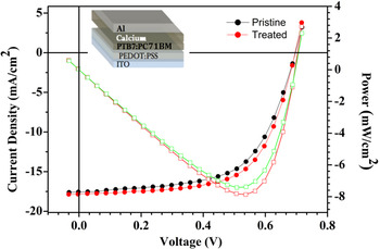
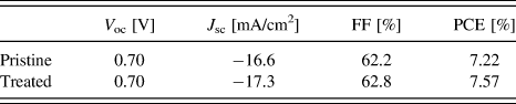
The general scheme of the OSCs used for the experiment is shown in the inset of Fig. 1. The studied system consists of the glass/ITO substrate, the PEDOT:PSS hole transport layer, the PTB7/PC71BM active layer and the Ca/Al electrode, which is in general an efficient contact to maximize the open circuit voltage V OC with polymer/fullerene systems for direct architectures. Reference Zampetti, Fallahpour, Dianetti, Salamandra, Santoni, Gagliardi, Auf der Maur, Brunetti, Reale, Brown and Di Carlo45 The use of Ca/Al as a contact with the PTB7:PC71BM blend in the same architecture like that proposed in this work has achieved an efficiency of about 9%, Reference Elshobaki, Anderegg and Chaudhary46 matching the record efficiency for PTB7:PC71BM blends. Reference He, Zhong, Huang, Wong, Wu, Chen, Su and Cao47 The integrated devices were characterized collecting J–V curves under the Sun simulator mentioned in Sec. II. A. The J–V characteristics of the as-deposited devices are shown in Fig. 1. The PV parameters extracted from the J–V curves are presented in Table I that compares short-circuit current (J SC), fill factor (FF), open circuit voltage (V OC), and power conversion efficiency (PCE) of pristine and vacuum treated devices.
J–V characteristics of the as-deposited devices (chart). General scheme of the OSC (inset).

PV parameters of the PTB7/PC71BM devices.

The values shown are average values obtained from J–V measurements performed on different devices. Evidence is provided that post-fabrication vacuum treatments have a beneficial effect on the initial PCE of the devices. These results are consistent with those in previous reports. Reference Susanna, Salamandra, Ciceroni, Mura, Brown, Reale, Rossi, Di Carlo and Brunetti41,48
To understand/interpret the OSC results, an insight into the molecular ordering of the photoactive layer and interfaces between different layers is needed.
B. EDXD/AFM analysis
An EDXD investigation was first performed to understand the effects of the vacuum treatment on the structural and morphological properties of the multilayered system with particular focus on the active layer. This goal was met by performing a systematic study via diffraction, AFM, and spectroscopic tools on the BHJ layer using the set of the devices manufactured without the metallic top electrode.
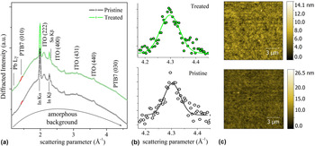
The diffraction spectra referring to the two as-deposited samples (pristine and vacuum treated) are depicted in Fig. 2 as a function of the scattering parameter q.
(a) EDXD spectra referring to the as-deposited pristine/treated PTB7/PC71BM samples, reporting the (010) PTB7 peak fit in red; (b) zoomed view of the PTB7 peaks fitted as Gaussian curves after background subtraction; (c) (10 × 10) m AFM images of the surfaces of the pristine/treated as-deposited PTB7/PC71BM samples.

In the low q region, the weak and broad diffraction peak arising from the blend at about q = 1.47(6) Å−1 is associated to the (010) diffraction of PTB7; this value, considering the error bar, complies with the 1.4–1.8 Å−1 range typically established for π–π stacking of such conductive polymers. Reference Szarko, Rolczynski, Lou, Xu, Strzalka, Marks, Yu and Chen49–Reference Zhong, Tuan Trinh, Chen, Purdum, Khlyabich, Sezen, Oh, Zhu, Fowler, Zhang, Wang, Nam, Sfeir, Black, Steigerwald, Loo, Ng, Zhu and Nuckolls56
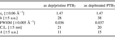
In particular, this peak results from the diffraction in the π–π stacking direction. It has already been demonstrated that PTB7 has a different preferential stacking orientation than other extensively used polymers, such as P3HT. Actually, P3HT shows an edge-on orientation on the PEDOT:PSS buffer layer. Reference DeLongchamp, Vogel, Jung, Gurau, Richter, Kirillov, Obrzut, Fischer, Sambasivan, Richter and Lin57 In contrast, polymers from the PTB family were proved to exhibit a face-on orientation on the PEDOT:PSS buffer layer, with planes parallel to the surface. Reference Lu and Yu58 This is a remarkable feature, given that the π–π direction plays a leading role in intermolecular charge transfer. Reference Sirringhaus, Brown, Friend, Nielsen, Bechgaard, Langeveld-Voss, Spiering, Janssen, Meijer, Herwig and de Leeuw59 Consequently, we examined how and how much the crystalline properties of the active layer of the pristine and vacuum treated samples differ one from another at the as-deposited stage, i.e., just after the deposition process and the vacuum treatment. The EDXD peaks were modeled as Gaussian curves following an amorphous background subtraction procedure. The data extracted from the best fit are presented in Table II.
Peak parameters extracted from the Gaussian best fits- x c: center position; h: intensity; FWHM: full width at half maximum; C.L.: coherence length; A: area.

The PTB7 π–π stacking distance is d = 4.3(1) Å and is the same for the two samples: no apparent lattice stress arose following the vacuum treatment. As a general concept, area, height, and width [typically one takes the full width at half maximum (FWHM)] of the diffraction peaks are strictly correlated with the crystallinity of the material; the peak height is representative of the crystallinity degree of the material and the FWHM is inversely proportional to the paracrystalline coherence length. Reference Paci, Generosi, Bailo, Rossi Albertini and De Bettignies28 Considering the error bars, all of the quantities extracted from the best fit calculations turned out to be comparable between the two samples. One can reasonably assert that the two specimens have very similar crystalline properties.
It should be noticed that a rough crystallinity estimation does not deliver “absolute values”, since different samples have been examined. However, the estimates are an important initial reference for the subsequent in situ study performed on the same samples.
The next step of the analysis involves the study of the morphological properties of the active layer. Knowledge and optimization of morphological features of the layers composing a PV device are essential factors, because they strongly influence the PV performance by modifying the interface electronic characteristics, the charge carriers’ mobility and thus the open circuit voltage. Reference Potscavage, Sharma and Kippelen60 They also produce effects on the stability (and hence lifetime), the interfacial regions being the most critical ones. Reference Steim, Kogler and Brabec61 To appraise possible consequences of the vacuum treatment on the physical arrangement of the active species at the surface of the film, a thorough AFM analysis was carried out [see Fig. 2(c)]. AFM images of the blend show a relatively flat surface except for a limited number of defects, which are likely to appear following the deposition process. The surface roughness (rms) extracted from the AFM data analysis is 1.3(1) nm for the pristine blend and 1.0(1) nm for the treated one: the samples substantially have similar surface structures and profiles, thus implying that the vacuum treatment did not cause significant morphology modifications of the active layer.
C. Time resolved EDXD and AFM analysis
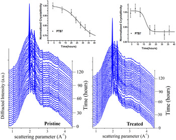
The in situ EDXD investigation consisted in acquiring a sequence of diffraction patterns collected every 4 h during illumination. Figure 3 shows the diffraction spectra evolution for the pristine and vacuum treated BHJ, respectively, as a function of the scattering parameter.
Time resolved EDXD for the pristine and treated BHJ under illumination. The inset reports the crystallinity trends as functions of illumination time for the pristine (left-hand side) and treated (right-hand side) samples, respectively.

The peak heights extracted from the fitting of each pattern allow evaluating the crystallinity behavior during illumination: the insets of Fig. 3 report the crystallinity trends versus illumination time for the pristine and vacuum treated BHJ, respectively.
The results show that PTB7 crystallinity decreases considerably over time: an insight into the crystallinity drop process was gained by modeling the experimental data trend using a Boltzmann sigmoid curve and deriving the temporal characteristics of the crystallinity time evolution. The sigmoid decrease of polymer crystallinity has a time constant of about 26 h. It can be seen that the crystallinity depletion process, starting a few hours after the light was turned on, resulted in a loss of about 30% after 40 h of illumination. A comparison can be made with the evolution of the vacuum treated sample during illumination time. In this case the time evolution of the diffraction spectra under illumination suggests that fullerene, very much like the pristine case, retains its initial overall crystallinity in the probed time range. On the other hand, during the same period of illumination, the loss of crystallinity of the polymeric component is much mitigated. It can be seen that the process is delayed, beginning only about 12 h after switching on the light and the crystallinity loss is only about 15% after 40 h. By fitting this trend with a sigmoid function, the time constant was found to be about 16 h.
Comparing the results obtained for the two samples, we can state that the polymer component is not stable under illumination, and for the pristine BHJ the drop in the total initial crystallinity is much larger (almost double) than its treated counterpart, after 40 h illumination. Also the crystallinity fall against time exhibits different kinetics in the two samples. In the pristine sample, the process starts immediately after turning on the light while in the vacuum treated sample it is slightly delayed.
The above observations are far from being obvious, considering that the samples presented very similar initial crystallinity. The vacuum treatment thus acts to stabilize the structure of the active blend and in particular of the BHJ polymeric fraction when submitted to lighting. This is a beneficial and desirable effect: indeed, one of the most impellent requirements to optimize polymer solar cells is finding pre- and/or post-production treatments that confer stability to the active layer, making it able to react to working conditions with negligible structural modifications.
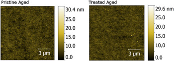
Figure 4 shows AFM images of the illuminated samples: it can be seen that in both samples the active material surface presents neither particular aggregates nor superstructures in relief.
AFM images of the aged pristine/treated samples (left- and right-hand side, respectively).

The roughness of these illuminated films was resolved: for the pristine sample a value of 1.3(1) nm is found; for its vacuum treated counterpart the roughness is estimated to be 1.0(1) nm. These are reasonably comparable values and are analogous to those detected for the as-deposited samples. It can be stated that the morphology of this new blend is not significantly affected by 40 h of illumination. This surprising result is in contrast with previous studies performed on OSCs based on other active systems such as the well-known P3HT/PC60BM pair. For this kind of BHJs, fullerene surface aggregates were found to build up after annealing or illumination processes Reference Paci, Generosi, Rossi Albertini and De Bettignies29 that were thought to deteriorate interface properties and consequently PV yields. Therefore, the above outcome is an important advance for the pressing requests to obtain durable and resistant PV devices.
D. FTIR analysis
The diffraction data have demonstrated that a simple vacuum treatment tends to stabilize the crystalline fraction of PTB7 under illumination. It is important to analyze the effects of the treatment also on the chemical stability of the two active materials after an aging process.
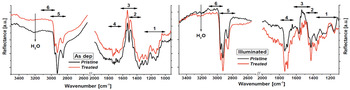
FTIR spectroscopy data, useful to detect possible chemical degradation of the used organic compounds, are reported in Fig. 5.
FTIR experimental curves: the as-deposited pristine (black line) and treated (red line) PTB7/PC71BM samples (left) and the effect of the illumination on the same samples (right).

The spectra of the two samples (pristine and vacuum treated) in the as-deposited and illuminated state are compared: it is evident that both samples underwent an outstanding and generalized degradation due to the illumination process.
All bands suffered a consistent intensity decrease, indicating that deterioration affects all the species of the active layer. This is an expected result: it is well known that light quickly and easily damages this kind of compounds. Reference Liu, Li and Yan62 Nevertheless, something more specific can be stated: the regions 1, 2, and 3 (see Table III) seem to be more affected by the intensity fall than the others; this effect is more evident in the pristine sample.
Attributions of the FTIR band vibrations.

Even though slightly, the vacuum treatment appears to reduce the extent of degradation of the active species. Another feature can be noted from the FTIR analysis: the spectrum corresponding to the illuminated/treated sample reveals sharper and clearer reflectance bands indicating that there is a more ordered structure in the treated blend.
This deduction agrees with the results obtained from the EDXD study for the higher crystallinity of the treated sample.
It must be highlighted that the specimen analyzed up to now is an intermediate device step without the second electrode capping the cell, to reach the active film with the AFM probe.
E. Space-resolved HR-XRD characterization of integrated devices
This section reports the results of the additional analysis conducted on the complete devices (glass/ITO/PEDOT:PSS/PTB7/PC71BM/Ca/Al system), based on HR-XRD measurements performed at the ID11 beamline (see Sec. II. C). In particular, the aim of this examination was to assess possible mutations of the active layer after operation and to evidence potential advantages deriving from a post-deposition vacuum treatment of the integrated devices. Firstly, the vacuum treatment effects on the as-deposited cells were examined for possible local structural differences. Secondly, the experiment was repeated on aged systems to point out the consequences of illumination and operation (under the Sun simulator mentioned in Sec. II. A) on both treated and untreated devices.
The structure and interface features of the OSCs were probed discriminating the contribution of each separate layer constituting the system by means of the HR-XRD setup and shifting the cell perpendicularly to the X-ray beam, i.e., from the ITO electrode up to the metallic cathode.
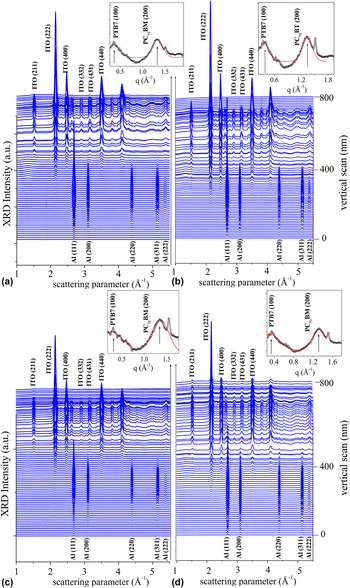
A vertical stack of diffraction maps along the cross section of each cell was recorded: Fig. 6 shows the sequence of XRD patterns (corrected for the parasitic scattering) collected during the scan of the four devices representing the “as-deposited” and “aged” states of both systems (pristine and treated), respectively.
Sequence of XRD patterns collected during the cross-sectional vertical scans of the four devices, representing the: (a) as-deposited pristine sample; (b) aged pristine sample; (c) as-deposited treated sample; and (d) aged treated sample.

The lower region corresponds to the Al film, while at higher vertical positions the ITO contribution is detected. Many diffraction peaks are visible and were accurately identified by extracting three distinct diffraction spectra referring to as many positions of the entire scan with the aim of isolating the contribution of Al electrode, BHJ layer, and ITO electrode, respectively. The peak identifiers are shown above or below each spectrum.
The peaks at q = 0.37(1) Å−1 and q = 1.33(1) Å−1 are associated to the Bragg reflections of the PTB7 lamellar stacking in the (100) direction and to the PC71BM (200) crystallites, respectively. Reference Wang, Kim, Seo, Park, Hong, Park and Heeger63–Reference Solé, Papillon, Cotte, Walter and Susini65 The π–π stacking of PTB7 was not detected, due to the presence in the same spectral region of all dominant crystalline contributions arising from the electrodes of the complete device.
The insets show the zooms of these peaks along with their Gaussian fitting curves. Their shape is characteristic of prevalently amorphous organic materials: they are very broad if compared with those associated to the crystalline ITO and Al lattices. The other peaks considered are the most intense and are related to the electrode response: the Al (111) and ITO (222) peaks at q = 2.686(1) Å−1 and at q = 2.144(1) Å−1, respectively.
This choice allows achieving an overview of the structural features of the multilayered system. As expected, the crystalline nature of calcium and PEDOT:PSS is not detectable, these two layers are thus excluded from the discussion about the diffraction behavior.
The data analysis consists in tracking the evolution of the four diffraction peaks of interest through the cross section of each sample, i.e., through the vertical scan. Peaks were fitted along the whole scan using Gaussian functions, the data processing procedure being fully described in Ref. Reference Paci, Bailo, Rossi Albertini, Wright, Ferrero, Spyropoulos, Stratakis and Kymakis44. In particular, the evolution of the peak intensities was studied to determine the crystallinity spatial trends.
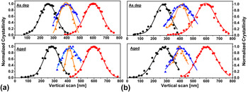
The normalized crystallinity spatial distributions of the diffraction peaks of Fig. 6 are depicted in Figs. 7(a) and 7(b), which compare the as-deposited and aged OSC devices for the pristine and treated systems, respectively. This data processing is necessary to plot the stratigraphic distribution, the contribution from the blend being much weaker (two orders of magnitude) with respect to those of the highly crystalline electrodes (as can be seen in the waterfall perspective, Fig. 6). Taking into account the 60 nm beam size and the vertical step size (10 nm), the interfaces between adjacent layers were probed by 6 ± 1 scans, corresponding to 8 patterns in Fig. 6 (and to 8 experimental points in Fig. 7). The few electrode points in the central part of the BHJ are characterized by relative signals intensities reduced to 0.5% of their maximum value and can be considered negligible compared to the PTB7 and PC71BM signals in the central part of the active layer.
Spatial trends of the normalized crystallinity as deduced by tracking the following diffraction peaks: black dot-Al (111); blue triangle-PC71BM (200); orange triangle-PTB7 (100); red dot-ITO (211). The continuous lines represent the Gaussian fits of the distributions. (a) refers to the as-deposited sample is analyzed, whereas (b) refers to the treated sample.

Considering the above-mentioned limits, it can be seen that the spatial distributions of the crystalline portions of the organic materials in the two as-deposited devices (treated and pristine) are comparable. Furthermore, the vacuum treatment does not seem to produce any clear phase intermixing.
These results are in agreement with the EDXD data that reveal similar structural and morphological properties among the as-deposited samples, suggesting that the vacuum treatment does not affect the crystalline properties of the system. Considering the crystallinity trends for the aged samples it can be observed that, generally, the interfaces both at the Ca/Al and ITO/PEDOT electrodes appear to be stable: there is no notable phase intermixing, at least of the crystalline phases, before and after device operation. In both samples, the signal arising from PC71BM appears to maintain the same spatial distribution across the BHJ in both pristine and vacuum-treated OSCs.
Remarkably, structural modifications become visible as a consequence of the continued illumination: analyzing the measured crystallinity values, it can be reasonably claimed that in both devices (treated and untreated) PTB7 undergoes a significant crystallinity decrease. Importantly, the reduction of the crystallinity amount along the organic film thickness is different in the two specimens. In the pristine device, a noticeable boundary effect has to be underlined: a conspicuous crystallinity loss is observed at the border regions of the active layer; this phenomenon produces a narrowing of the crystallinity spatial distribution toward the interfaces of the BHJ, visible in Fig. 7. Such an enhanced decrease of crystallinity at the interface between the BHJ and the Ca/Al electrode is not observed in the treated device.
This localized stabilization at the buried cathode interface can be ascribed to the beneficial effects of the vacuum treatment, as corroborated by the FTIR analysis; the vacuum treatment triggers the removal of the residual solvents (chlorobenzene and 1,8-diiodooctane) and water from the active layer. It is well known that calcium is very sensitive to water Reference Norrman, Gevorgyan and Krebs66 and quickly undergoes degradation, Reference Poh, Sanek, Ambrosi, Zhao, Sofer and Pumera67 thus the reduced presence of water in the treated device compared to its pristine counterpart may account for the stabilization of the interface between the active layer and the Ca/Al electrode promoting the polymer crystallinity stabilization near the interface. Further analysis was carried out on the spatial crystallinity distributions: the areas underneath the Gaussian curves were evaluated. Based on their estimation, the overall crystallinity losses of the as-deposited and aged devices could be qualitatively compared. From such evaluation, it emerges that in the pristine specimen the overall crystallinity drop of PTB7, resulting from the aging of the integrated device, amounts to about 30%, while in the treated sample the overall polymer crystallinity reduction is about 10%.
Although the HR-XRD investigation was made on different samples (namely the complete devices and not the BHJ films), the results are in good agreement with the crystallinity loss estimation resulting from the in situ EDXD analysis. The above findings suggest that the vacuum treatment is unable to totally prevent the degradation process during illumination and operation of the cell: the treated sample shows greater resistance to the crystallinity downturn process induced by illumination and operation. Therefore, the data indicate that the effect of treatment is a substantial stabilization.
In particular, the treatment proved to induce an enhanced durability of the active film toward the interface with the Ca/Al electrode, this being a far-reaching property for applications. It must be stressed that this result is a paramount outcome since the buried cathode interface is one of the most critical regions of such a multilayered system, strongly influencing the efficiency and lifetime of an organic PV device.
F. PV aging
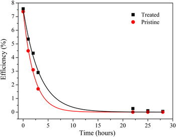
Owing to the above encouraging results, we also studied the effect of post-fabrication vacuum treatments on the OSC device’s durability: the OSCs were aged under a light soaker’s continuous illumination for 27 h in open circuit mode without encapsulation, in order for humidity to directly affect their performance. The evolution of the respective PV parameters versus exposure time was monitored for both tested devices: for each data point of the aging curves, a complete J–V characteristic was recorded and the normalized J SC, FF, V OC, and PCE values were subsequently calculated.
In both cases, degradation of the performances was observed, which can be imputed to the effect of humidity on the Ca/Al contact when the devices are not encapsulated (see Fig. 8). Reference He, Zhong, Huang, Wong, Wu, Chen, Su and Cao47,Reference Lloyd, Olson, Lu, Fang, Moore, White, Reese, Ginley and Hsua68
IV aging curves for the pristine/treated devices exposed to continuous illumination from a light soaker.

However, for the pristine device, the PCE after 3 h of aging was detected to be approximately 23% of the initial value.
Conversely, the treated device preserved 38% of its initial PCE. In general, for the treated cell, the degradation rate measured on the same time scale is much slower, revealing the benign role of vacuum treatments in protecting layers against degradation.
Summarizing, the vacuum treatment promotes the stabilization of the crystalline fraction of the active materials, reflecting on the maintenance of the initial structural arrangement of the BHJ materials. The consequence of this fact is the ability of preventing the optimized initial blend architecture from being quickly deteriorated under illumination, therefore allowing for a better preservation of the PV performances. Thus, the results provide evidence that the use of vacuum treatment contributes to protecting the device from the morphological modifications induced by working conditions, i.e., one of the degradation pathways responsible for device fading.
IV. CONCLUSIONS
The present research focuses on the effect of vacuum treatment on the structural and morphological properties and stability of OSCs based on a PTB7/PC71BM BHJ. For this purpose, two complementary techniques, i.e., time-resolved EDXD and HR-XRD, are applied to OSC devices: the results reveal that this unconventional approach is a powerful tool for the successful identification of aging routes related to bulk and interface structural properties.
Specifically, the vacuum treatment does not affect the initial structural properties of the acceptor/donor blend and enables removing residual moisture without perturbing the active film structure and morphology. Furthermore, aging studies under illumination target the morphological stability of the systems: the surface roughness remaining stable and no aggregates being visible on the surface in both pristine and treated aged samples. On the other hand, in situ EDXD shows that illumination affects the polymer component triggering a crystallinity decrease. This effect is much mitigated in the treated sample that appears to be significantly more stable.
Additionally, via space-resolved HR-XRD on the integrated devices interesting information is gathered on the local modification of the active blend as a consequence of device operation. It is recognized that in both the pristine and vacuum treated devices PTB7 loses part of its initial crystallinity (in agreement with EDXD results), but the spatial features and the extent of this loss is very different in the two cells. The polymer crystallinity spatial trend in the pristine device shows significant interface degradation. Conversely, in the treated device, the crystallinity drop is inhibited, particularly at the BHJ interface with the Ca/Al electrode; this result suggests that the vacuum treatment is able to locally preserve the active film/cathode interface. This stabilization capability is likely to be due to the water removal as observed by FTIR analysis.
In conclusion, the vacuum treatment augments the stability of the polymer/fullerene blend, limiting the deterioration of the bulk architecture upon illumination and operation and strengthening the buried interface with the Ca/Al cathode. This advantageous effect reflects on the PV properties, reducing device aging under working conditions.
ACKNOWLEDGMENTS
The authors are greatly indebted to Jonathan P. Wright for his invaluable help in performing the HR-XRD experiments. The authors acknowledge the European Union under Contract No. 309201 “GO-NEXTS”.