
Introduction
Organic thin films have attracted great interest due to their ability to interact with surfaces, tailoring specific properties for a myriad of applications.[Reference Richardson, Björnmalm and Caruso1] In this context, the layer-by-layer (LbL) technique is a simple method to modify large area surfaces.[Reference Decher, Hong and Schmitt2] This method forms multilayered nanostructured films by spontaneous adsorption of polyelectrolytes due to non-covalent intermolecular interactions (electrostatic, van der Waals, and hydrogen bonding). LbL film properties such as optical absorption,[Reference Dey and Pal3] roughness,[Reference Sakai, Webber, Vo, Wanless, Vamvakaki, Bütün, Armes and Biggs4] and conductivity[Reference Granholm, Paloheimo and Stubb5] depend on the assembled materials, the way they are nanostructured, and the number of adsorbed layers,[Reference Wang, Cao, Tagaya and Kobayashi6] demanding a precise control of the adsorption process during the LbL assembly. Consequently, new methods and instruments are fundamental to precisely track the film properties during the LbL growth at each deposited layer, independently of adsorption steps.
The use of capacitive devices such as electrolyte–insulator–semiconductor (EIS) capacitor to analyze DNA immobilization and hybridization inspired their use to monitor LbL film growth.[Reference Fritz, Cooper, Gaudet, Sorger and Manalis7, Reference Poghossian, Abouzar, Sakkari, Kassab, Han, Ingebrandt, Offenhausser and Schoning8] As an example, Poghossian et al. tracked the growth of LbL films formed by poly(allylamine hydrochloride) (PAH) and poly(sodium 4-styrenesulfonate) (PSS) in a (PAH/PSS)n architecture (n being the number of deposited bilayers) by means of capacitance as a function of voltage measurements (C–V) on EIS devices after each deposition step.[Reference Poghossian, Weil, Cherstvy and Schöning9, Reference Poghossian, Weil and Schöning10] The observed alternation in the polarization voltage according to the deposited polyelectrolyte layer demonstrated a dependence between the polarization voltage amplitude displacement as a function of NaCl concentration in the polyelectrolytes solutions.[Reference Poghossian, Weil, Cherstvy and Schöning9]
Moreover, Daikuzono et al. monitored LbL films formed inside microchannels filled with aqueous solutions passing on interdigitated electrodes (IDEs), without salt added to the polyelectrolyte solution.[Reference Daikuzono, Dantas, Volpati, Constantino, Piazzetta, Gobbi, Taylor, Oliveira and Riul11] They also observed capacitance zig-zag-like behavior as previously reported in the literature,[Reference Poghossian, Weil, Cherstvy and Schöning9, Reference Ladam, Schaad, Voegel, Schaaf, Decher and Cuisinier12] with a linear capacitance increase using poly(pyrrole) (PPy) as polyanion and a linear capacitance decrease after replacing PPy by nickel(II) phthalocyanine-tetrasulfonic acid tetrasodium salt, using PAH as the positive polyelectrolyte in both cases.
Despite the contribution of these methodologies, the electrical properties of the LbL films can be strongly influenced by the environmental conditions, such as aqueous and salty media.[Reference Poghossian, Weil, Cherstvy and Schöning9–Reference Daikuzono, Dantas, Volpati, Constantino, Piazzetta, Gobbi, Taylor, Oliveira and Riul11] Salt or aqueous solutions can inherently limit the number of layers that can be characterized. Here we present a new methodology and the corresponding automated setup to measure the capacitance of as-deposited LbL films in the air right after the material adsorption. This method is able to verify the film stabilization during the spontaneous drying process in the air and also measure changes in the electrical signal with high accuracy (~0.01 pF) and reproducibility in the formed multilayered nanostructures.
Instruments
The LbL technique by dipping deposition allows for self-assembled ultrathin films that can be carried out even manually. However, in order to increase the reproducibility, it is wise to control the substrate movement in polyelectrolyte solutions during immersion and rinsing steps.[Reference Clark and Hammond13] There are several commercial equipment available for this purpose; nonetheless, they do not allow ease integration with electrical measurements, which is fundamental to better comprehend the film formation, mainly if the optical characterization is not suitable. To overcome this difficulty, we present an instrument to perform LbL film growth independent of the number of deposited layers, totally integrated with a capacitance meter that analyzes the film fabricated after each deposition step, tracking the film formation and simultaneously analyze its electrical properties in the air.
Automated dipping LbL
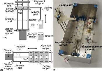
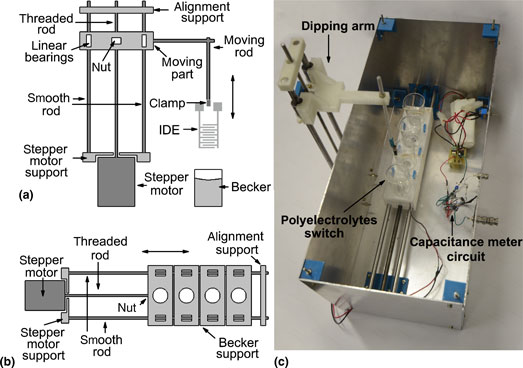
Figure 1 presents a scheme of the automated setup developed to perform dipping LbL assembly. The structural parts were made by acrylonitrile butadiene styrene using a fused deposition modeling three-dimensional printer. The setup illustrated in Fig. 1(a) is responsible for the dipping process and it is composed by two structural pieces that promotes the system alignment. One of them is fixed on a stepper motor, which is coupled to a threaded rod. The threaded rod rotation smoothly moves a nut fixed on the moving part promoting the desired linear motion. The stepper motor control was implemented using an Arduino UNO and a Pololu A4988 driver that fractionate the motor step until 1/16. Our aim was achieving 10 mm/min dipping speed with a smooth movement, which was possible adjusting the driver to fractionate the motor step by 1/8, obtaining 1600 steps/turn, which allows for the desired velocity with a threaded rod nut moving 0.8 mm/turn.
Automated dipping LbL films growth system: (a) side view scheme for immersion and emersion movement; (b) top view scheme for polyelectrolytes switch; (c) home-made built setup.
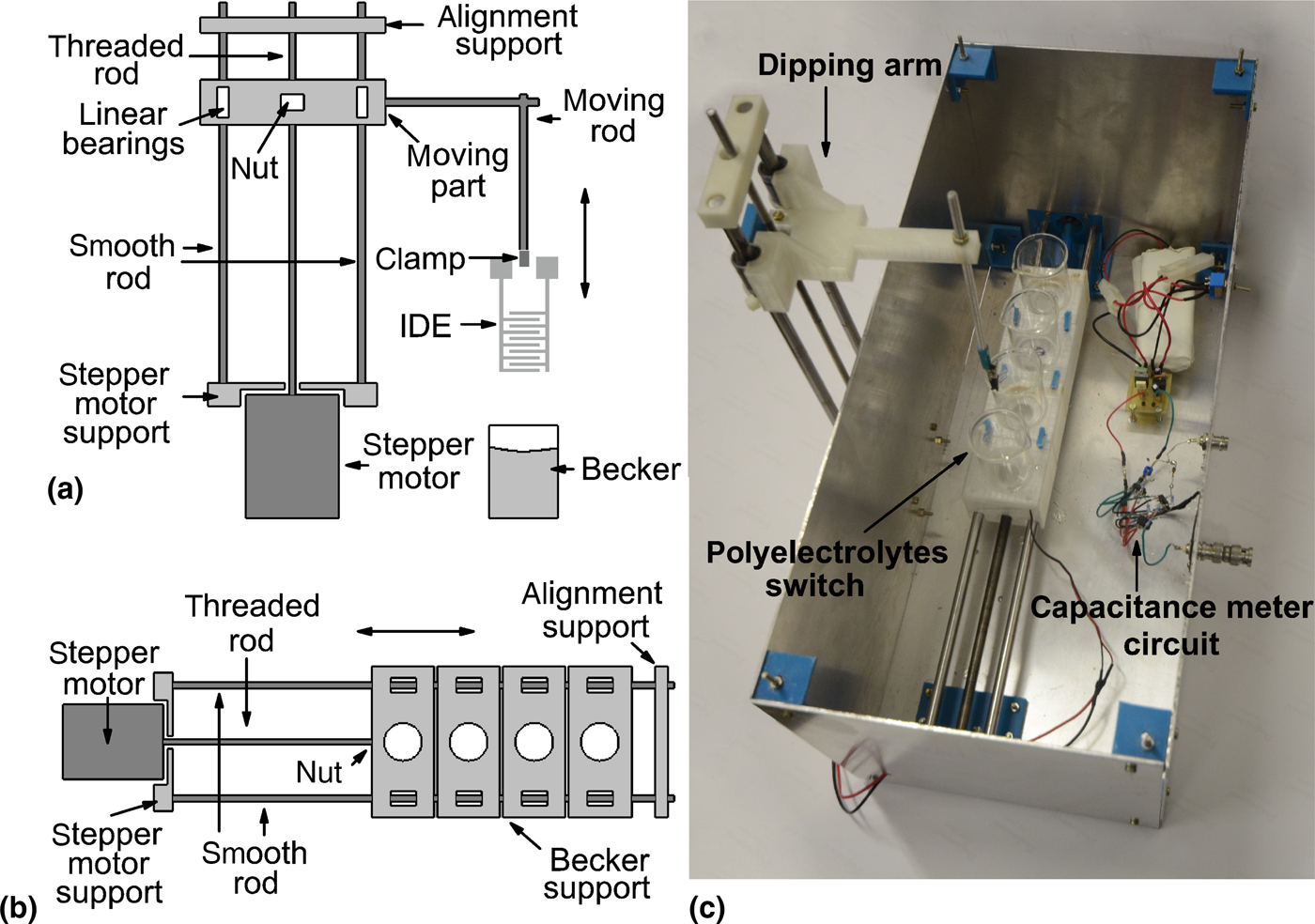
The LbL multilayer formation requires the sequential deposition of polycations and polyanions and, to minimize the film defects due to material loosely bound and decrease cross-contamination of the polyelectrolytes, a rinsing step between each adsorption step was used. To automate this process, we implemented a Becker switch setup that operates in close analogy to the mechanical dipping arm. The moving part was replaced by four pieces to support the Becker as shown in Fig. 1(b). We chose to use two independent systems to dip clean the substrate and to change the Becker to assure the wires connecting the electrode for electrical measurements would not break during the experiments and also to avoid capacitance variation introduced by the wires movement. The same Arduino UNO controlled dipping arm and Becker switch. Furthermore, we developed a graphic interface using Tcl/Tk to control the automated LbL dipping setup in order to integrate it with the capacitance meter system.
This setup can become useful to grow self-assembly films automatically for a myriad of experiments. Its versatility to control the immersion velocity due to stepper motor and Pololu A4988 driver use allows for making immersion process faster and also useful in kinetics experiments, for example.[Reference Ferreira, Gomes, Maneira, Ribeiro and Raposo14]
Capacitance meter
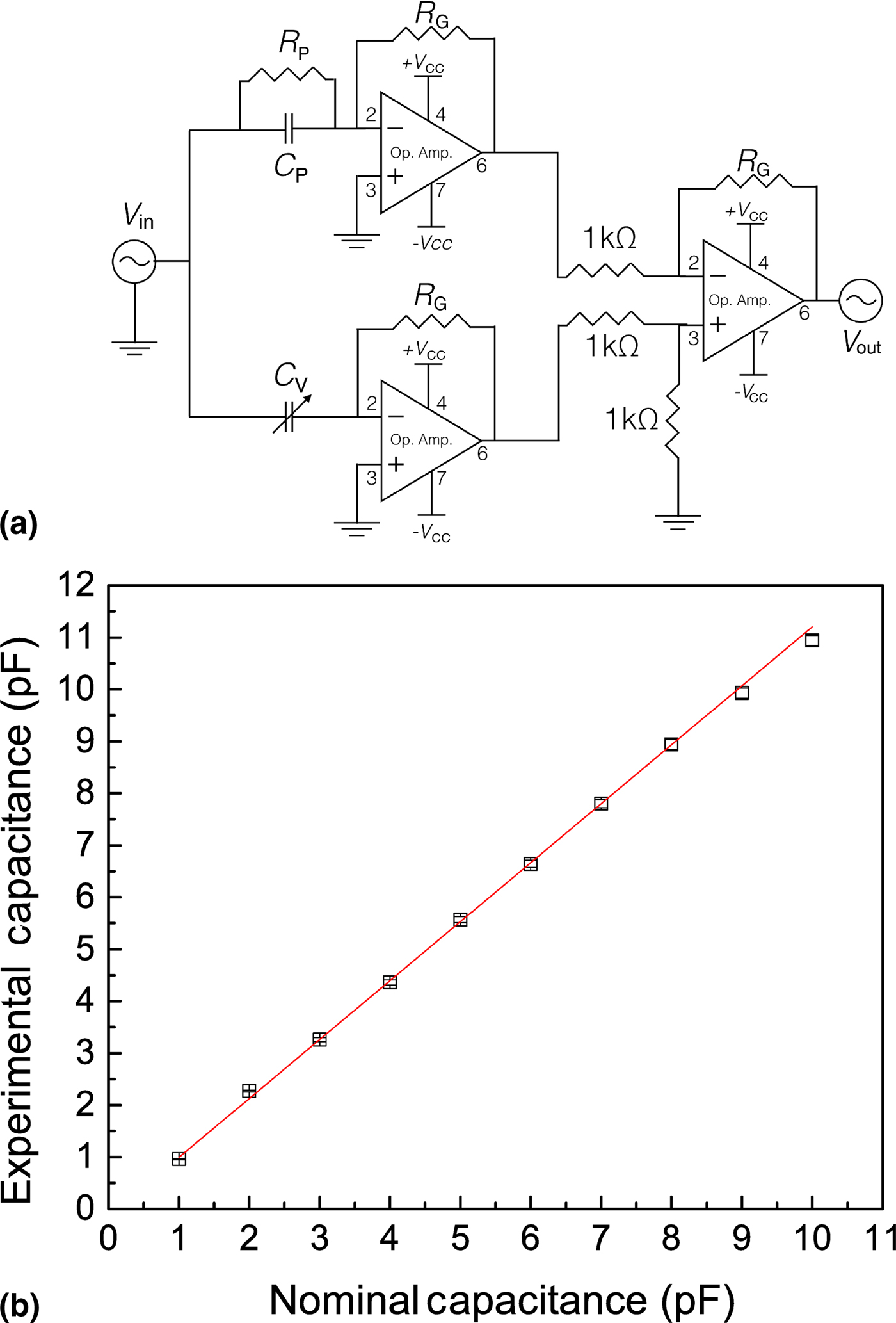
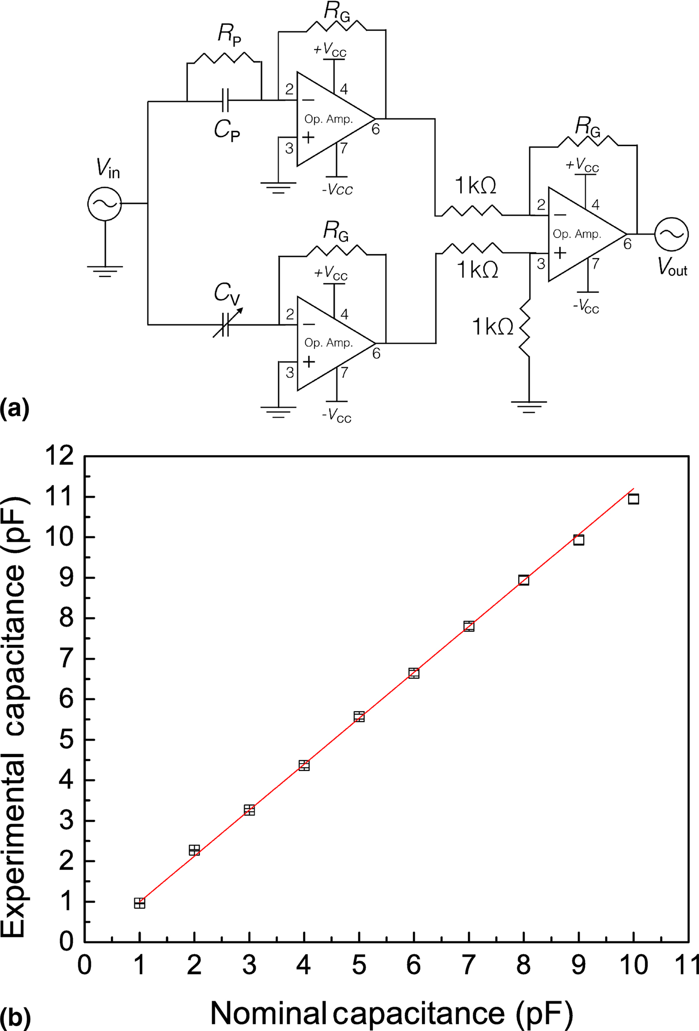
The capacitance meter was developed according to the scheme showed in Fig. 2(a). It consists of two operational amplifiers (Op. Amp.), on the left, that operates as current to voltage converters (IV converters). One acts on the current provided by the sample, modeled as a capacitor C P in parallel to a resistor R P. The other one acts on the current provided by a variable capacitor C V, which is used to compensate any parasitic capacitance on the IV that acts on the sample. The same AC input voltage V in with amplitude V 0 and frequency f excites both capacitance branches. The Op. Amp. on the right provides the difference between the two IV converters. To compensate for a parasitic capacitance in C P, we set the variable capacitor C V so that the output voltage V out cancels out. Therefore, associating the device of interest C i in parallel to C P, the output voltage amplitude A as a function of C i is given by Eq.(1), in which ω = 2πf, ϕ is the phase shift between the input and output voltages, and R G = 82 kΩ is the feedback Op. Amp. resistance.
 $${\bi A} = {\bi V}_0 {\bi R}_{\bf G} {\bi \omega}\;{\bi C}_{\bf i} \sqrt {\displaystyle{1 \over {\tan ^2 \phi}} + 1}. $$
(a) Capacitance meter's circuit composed by two IV converters on the left and a comparator circuit on the right. The variable capacitor C V compensates a parasitic capacitance in C P, minimizing the output voltage V out. Associating the device of interest C i in parallel to C P, its capacitance can be obtained measuring the output voltage amplitude A and phase shift between V in and V out; (b) experimental capacitance measured using the capacitance meter on commercial capacitors to verify the circuit performance.
Moreover, to reduce parasitic capacitances due to the circuit assembly, the components were directly welded to each other, maintaining the maximum geometric symmetry. The continuous voltages supplying inputs 7 and 4 of the three Texas Instruments LMC6001BIN Op. Amp. are provided by a symmetrical source composed of two batteries, voltage regulators (7806 and 7906) and capacitors, as specified in the voltage regulators datasheet.
We have characterized the capacitance meter using a RS830 Stanford Research Systems lock-in amplifier, V in = 1 V in amplitude at 2 kHz, provided by the lock-in internal source, and ten 1 pF commercial capacitors associated one by one in parallel to the C P. After each association, the output voltage amplitude and the phase between input and output signal using lock-in technique were acquired. The dependence between the experimental and nominal capacitance is presented in Fig. 2(b). The linear fit slope 1.13 ± 0.02 confirmed the correspondence between nominal and measured capacitance, so we could infer an excellent performance on the circuit operation.
Methodology
Sample preparation
For the LbL deposition, we deep clean the substrate surface to favor the spontaneous adsorption of molecules from the polyelectrolyte solutions.[Reference Decher, Hong and Schmitt2] To do so, we performed a hydrophilization process[Reference Kern15] that removes organic contaminants, turning glass and quartz surfaces negatively charged. After this procedure, the clean substrates were rinsed with ultrapure water provided by an Arium Comfort Sartorius system and dried with a gentle nitrogen flow.
The LbL film was obtained using poly(diallyldimethylammonium chloride) (PDDA) as polycation and copper phthalocyanine-3,4′,4″,4″′-tetrasulfonic acid tetrasodium salt (CuTsPc) as polyanion, both acquired from Sigma-Aldrich and used as received. PDDA solutions were prepared using 5 µL/mL of ultrapure water. Furthermore, CuTsPc solutions were performed using 0.5 mg/mL of ultrapure water. Both solutions pH were controlled using a PG 1800 GEHAKA pH meter and adjusted to 8 using 0.1 M HCl and 0.1 M NaOH solution.[Reference Daikuzono16]
The dipping arm was set to an immersion speed of 60 mm/min and the emersion speed was set to 10 mm/min to ensure that the LbL film left the polyelectrolyte solutions almost dried. The LbL deposition started with the positively charged polyelectrolyte. All polyelectrolyte emersions were followed by a rinsing process with ultrapure water to remove the material loosely bound, in a different Becker for each polyelectrolyte type. This sequential process resulted in a multilayered (PDDA/CuTsPc)n film that was then optically and electrically characterized.
Optical measurements
In order to verify that our setup was able to track the self-assembly thin film formation, we compared the capacitance measurements by the integrated LbL/capacitance meter with UV–vis absorption spectroscopy for each deposition step.
(PDDA/CuTsPc) LbL films were deposited onto quartz plates and optically characterized by a S50 visible ultraviolet spectrometer from Biochrom Libra. The LbL film optical absorption was analyzed using the CuTsPc Q band at 619 nm.
Capacitance measurements
As previously mentioned, our setup was able to investigate the LbL capacitance evolution in the air to avoid external interferences provided by salt and/or aqueous media. To do so, we used a 3.3 pF commercial capacitor as the C P and applying an AC signal 1 V amplitude at 2 kHz to the capacitance meter circuit. Then, we have adjusted the variable capacitor C V to minimize the output voltage amplitude. Gold IDEs on glass, composed by 30 pairs of digits 3 mm length, 40 µm width, and spaced 40 µm each other (cell constant ~ 88.5 mm), were welded in parallel to the C P capacitor. By measuring the output voltage amplitude and phase shift between the input and output voltages, it was possible to calculate the IDE capacitance using Eq. (1). All IDEs used in this work were produced at Microfabrication Laboratory in Brazilian Nanotechnology National Laboratory (LNNano/CNPEM).
We have also implemented a methodology to evaluate the capacitance evolution after each PDDA and CuTsPc layer deposition onto the IDEs to decide when to measure the capacitance after finishing the deposition of the newest layer. This procedure was necessary to improve the capacitance accuracy as we observed that it varies after each formed bilayer due to the presence of weakly bound water molecules trapped in the as-deposited LbL multilayer. Based on the output voltage and phase shift for each measurement, starting immediately after the layer deposition, we calculated the capacitance using Eq. (1) at 500 ms intervals. When the average dispersion of the last 100 measurements gets lower than 0.01 pF, the data acquisition is interrupted and the last capacitance average value is salved. If this dispersion limit is not reached within 600 s, the acceptable deviation for the average capacitance increases to 0.02 pF and if the minimum deviation is not reached within 800 s then it increases to 0.05 pF.
Results
The aim of this work was the study of electrical properties evolution as a function of the number of LbL deposited layers, using a simplified setup with no need of trained person. However, we observed that it takes certain time for the measurements stabilization after IDEs rinsing step. To understand how to deal with this stabilization time in our measurement, we have analyzed the capacitance time evolution immediately after the electrode leaves the water.
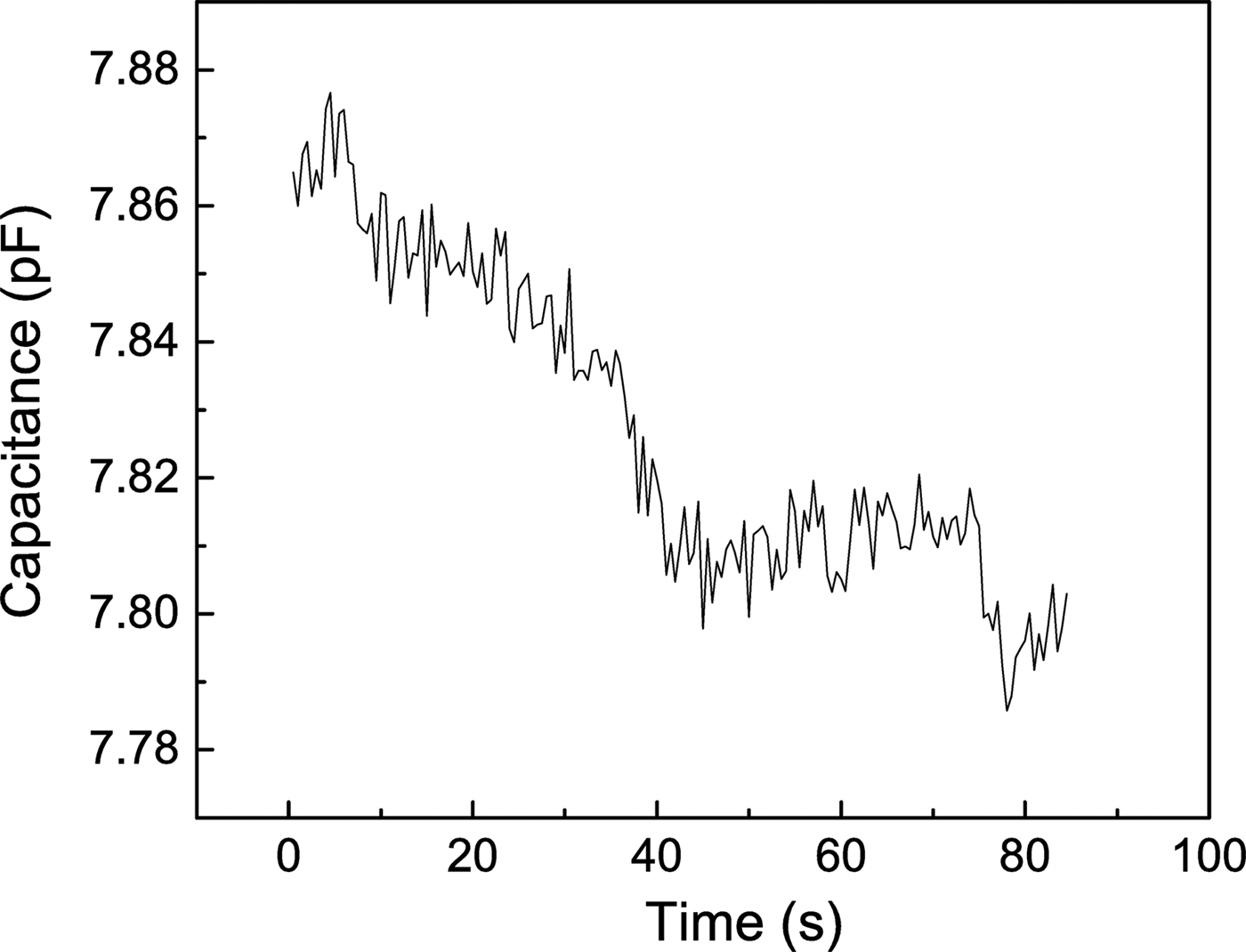
Figure 3 shows a typical capacitance time evolution after the PDDA rising step of a self-assembled films. The graph shows the capacitance variation in time, which oscillates until converge to a value which satisfied the dispersion limit, defined in ‘Capacitance measurements’ section, after 85 s.
Capacitance variation as a function of time to illustrate the method developed to evaluate the capacitance stabilization and increase the measurements accuracy.

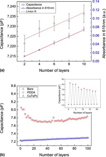
To verify the capability of our setup to monitor the LbL film formation, we also analyzed the film formed onto quartz plates by UV–vis absorption spectroscopy. Fig. 4(a) shows a comparison between the capacitance and UV–vis measurements at 619 nm[Reference Wang, Zheng, Qiao, Qu and Cao17] for the first five (PDDA/CuTsPc) deposited bilayers. It was possible to observe a linear increase in both capacitance and absorbance values with the number of deposited layers. Such behavior is associated with the dielectric material deposited onto the quartz plate and IDEs at the same rate in each deposition step, characteristic of the molecular-level thickness control provided by the LbL technique. The optical measurements were performed in duplicate and the electrical in triplicate, so we can also infer good reproducibility in LbL film formation due to fine control in the substrate vertical movements by the developed mechanical arm.
(a) Comparison between capacitance and absorbance as a function of the number of bilayers deposited on IDE (left side) and quartz (right side): linear increase with the number of adsorbed bilayers for both techniques; (b) capacitance measurement with the number of layers deposited on IDE: linear increase with the number of bilayers with a zig-zag-like behavior due to charge overcompensation of the outermost layer; inset: zoom-in to show the zig-zag-like behavior.
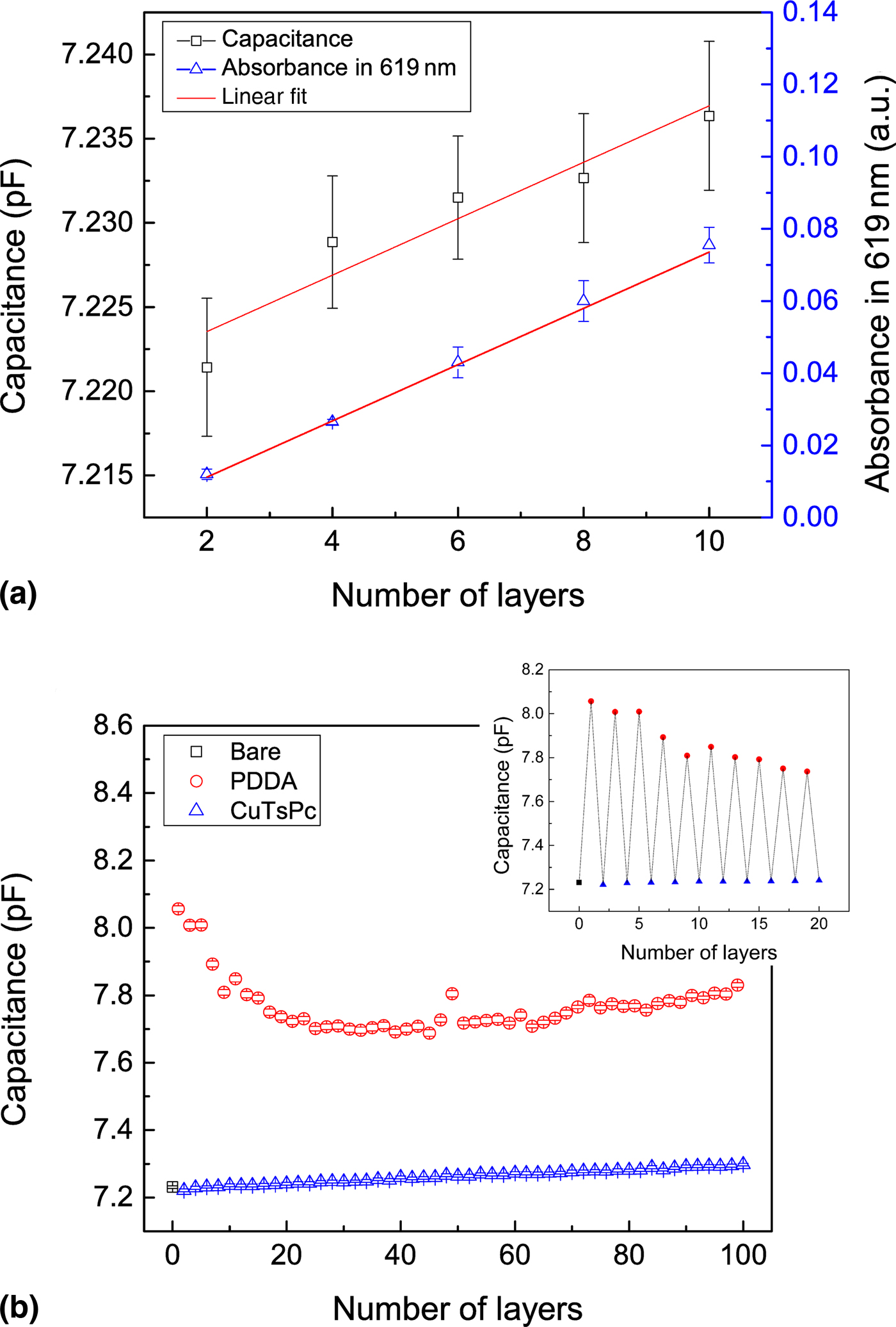
Considering capacitance measurements acquired after each deposited layer as shown in Fig. 4(b), we can clearly observe an alternation in the capacitance values, i.e., whenever the multilayer structure outermost layer is composed of PDDA, there is an increase in the measured capacitance, which is compensated after the adsorption of the next CuTsPc layer. This effect is well known on literature for ς potential[Reference Sakai, Webber, Vo, Wanless, Vamvakaki, Bütün, Armes and Biggs4, Reference Ladam, Schaad, Voegel, Schaaf, Decher and Cuisinier12] and capacitance[Reference Poghossian, Weil, Cherstvy and Schöning9, Reference Daikuzono, Dantas, Volpati, Constantino, Piazzetta, Gobbi, Taylor, Oliveira and Riul11] measurements performed in aqueous media and has been related to charge reversal on the multilayered structure. Therefore, our automated setup can monitor the charge reversal of the outermost layer in LbL films even when the substrate is not immersed into electrolytes.
In addition, we observed that the bilayer capacitance increases linearly with the number of layers, as depicted in Fig. 4(b), corroborating previous results from the literature that the same amount of material was adsorbed at each deposition step. Furthermore, our experiments did not reproduce the case reported by Daikuzono et al., in which a negative capacitance slope was observed for LbL capacitance monitoring using phthalocyanines as polyanion.[Reference Daikuzono, Dantas, Volpati, Constantino, Piazzetta, Gobbi, Taylor, Oliveira and Riul11] We attributed this difference to the fact that our measurements were taken in the air. To illustrate, at the beginning of the experiment, the electrode is immersed in the air, so after the first layer deposition, part of the air layer is replaced by the film. In this case, the capacitance increases because the film permittivity is greater than the air. In the case the measurements were performed in the water, for which dielectric constant is approximately 80, after each layer deposition, part of the water layer is replaced by the film, for which dielectric constant is smaller than the water. As a consequence, the capacitance decreases with the film deposition as observed by Daikuzono et al.[Reference Daikuzono, Dantas, Volpati, Constantino, Piazzetta, Gobbi, Taylor, Oliveira and Riul11]
Conclusions
We described here a methodology and experimental setup that was successfully integrated with a capacitance meter to automate the LbL film fabrication. The setup presented high accuracy (~ 0.01 pF) and reproducibility, being able to evaluate the capacitance evolution during the spontaneous drying process of the LbL films in the air after each deposition step. (PDDA/CuTsPc)n films were monitored up to 50 bilayers with capacitance measurements taken in the air to avoid influence from liquid systems during data acquisition. The experiments allowed for a precise monitoring of each deposited layer and also observe the capacitance zig-zag-like behavior even after rinsing and spontaneous drying steps. The method proposed here can become a valuable tool to study the electrical properties in nanostructured materials, opening up new prospects to study materials nanostructuration during the LbL film formation, affording the appropriate choice of materials, thickness, and molecular architecture for specific applications.
Acknowledgments
The authors are grateful to FAPESP (2014/03691-7), CNPq, and CAPES for financial support, and Microfabrication Laboratory in Brazilian Nanotechnology National Laboratory for the experimental support.