I. INTRODUCTION
Due to the fast growing popularity of the wireless communication systems, high efficiency power amplifiers (PAs) have become one of the most important components in modern RF transmitters. Since high efficiency leads to lower power consumption, smaller battery size, and reduced cooling requirements, the efficiency has become one of the most important design parameters, not only for hand-held terminals where the power is generated from a limited power supply, but also for base station applications where it can reduce the amount of wasted energy [Reference Cripps1].
By careful design of the transistor load network in the PA, it is possible to produce voltage and current waveforms that do not overlap. As a result, in these so-called switched mode power amplifiers (SMPAs), there is no power dissipation across the transistor and theoretically 100% efficiency is achieved [Reference Raab2]. In practical high-frequency SMPAs, however, the efficiency is degraded from 100% due to non-idealities of the components. Typical non-idealities are parasitic elements, finite on-resistance, non-zero transition time, and non-zero knee voltage.
Regarding the active device, silicon laterally diffused metal oxide semiconductor (Si LDMOS) has been the best candidate at frequencies around 1 GHz. However, its performance limited in the high-frequency region due to its relatively large output capacitance. Wide-bandgap devices such as gallium nitride high electron mobility transistor (GaN HEMT) overcome this problem and provide high electron mobility, high current density, and high breakdown voltage. The GaN HEMT has been addressed as a substitute for Si LDMOS [Reference Pribble3, Reference Nagy, Brown, Borges and Singhal4].
One specific type of SMPA that has recently attracted a lot of attention in high-frequency applications is the inverse class-F. Analysis and experiments, which demonstrated advantages of the inverse class-F amplifier, have been reported in [Reference Inoue, Ohta, Goto, Ishikawa and Matsuda5–Reference Woo, Yang and Kim8].
Recently, we have presented in [Reference Saad, Nemati, Thorsell, Andersson and Fager9] state-of-the-art high-efficiency microwave PA which is based on the inverse class-F configuration. The design is based on a harmonic load-pull simulation approach and the design of a suitable matching network.
In this paper we present an extension of [Reference Saad, Nemati, Thorsell, Andersson and Fager9], where the model used has been presented and evaluated by comparing simulations with the measurement results. Moreover, the PA performance has been more investigated by performing more measurements like large signal return-loss and modulated measurements using different types of signals.
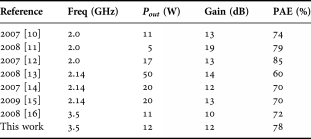
Comparisons between the performance of the presented PA with state-of-the-art results for GaN PAs are summarized in Table 1. The outstanding performance of the PA presented verifies the success of the design procedure adopted.
State-of-the-Art SMPAs using GaN HEMTs technology, f ≥ 2 GHz and P out ≥ 5 W

This paper is organized as follows. Section II gives a brief overview of inverse class-F PAs. An overview of the transistor model and the design procedure used for the PA is given in Section III. The implementation of the PA and the measurement results are presented in Section IV and finally conclusions are given in Section V.
II. INVERSE CLASS-F PAs
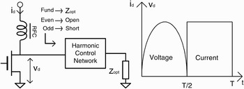
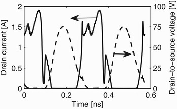
All high-efficiency PAs are based on careful control of the harmonic content of the voltage and current waveforms at the transistor intrinsic terminals. The construction of an ideal inverse class-F PA consists in imposing a square and half-sinusoidal waveform for drain-current and drain-to-source voltage, respectively. Figure 1 presents the drain-current and drain-to-source voltage waveforms.
Current and voltage waveforms for an ideal inverse class F PA.

These idealized waveforms are obtained by control of the transistor load impedance at different harmonics. The optimum resistive load impedance must be matched to the system impedance (Z c) at the fundamental frequency. Moreover, the output impedance seen by the device at even harmonics has to be open circuited because the half sine voltage wave only consists of even harmonics. On the other hand, all odd harmonic impedances must be short circuited in order to approximate a square drain current. According to [Reference Raab17], the second, 2f 0, and third, 3f 0, harmonics are most important for high-efficiency operation. In [Reference Negra and Bachtold18], it is shown that controlling these two harmonics is usually enough in practical microwave PAs.
Furthermore, controlling more harmonics increases circuit complexity without necessarily improving the performance [Reference Negra, Ghannouchi and Bachtold19]. On the contrary, manipulation of excessive harmonics may reduce the bandwidth of the PA. Thus, close to optimal, load impedances are given by:



where f 0 is the fundamental frequency and Z opt is the optimal load impedance at the fundamental frequency.
III. DESIGN METHODOLOGY
In order to reduce the parasitics of the package and facilitate harmonic impedance optimization at the transistor output reference plane, a bare-die, Cree CGH60015DE GaN HEMT is used.
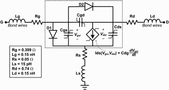
In SMPAs and harmonically tuned amplifiers, the transistor operates in the on- and off-regions. A simplified transistor model optimized for this type of operation is developed and used in the PA design. The model is based on simplified expressions for the nonlinear currents and capacitances where focus is put on accurately predicting the high efficiency, on- and off-regions of the transistor characteristics. The model allows the intrinsic waveforms to be studied in the PA design and therefore allows a careful investigation of the transistor operation. More details about the modeling approach used are given in [Reference Nemati, Fager, Thorsell and Herbert20]. In contrast to the model in [Reference Nemati, Fager, Thorsell and Herbert20], where an LDMOS model was used, diode models are added in this case to accurately predict forward gate voltage and negative drain voltage conditions of a GaN transistor. The topology of this model is shown in Fig. 2.
Large signal GaN HEMT equivalent circuit model.

The first step to design the PA was to find the optimum input and output load conditions to maximize the output power and efficiency of the transistor. The procedure for optimization of the fundamental and harmonic impedances is summarized as below:
1) Perform a fundamental load-pull/source-pull simulation to find the optimum fundamental load and source impedances for efficiency and output power.
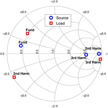
2) Using the impedances found in the previous step, a harmonic load-pull simulation was performed to find the optimum second and third harmonic load and source impedances for high-efficiency operation. The obtained optimum source and load impedances at fundamental, second, and third harmonics that maximize the power-added efficiency (PAE) are shown in Fig. 3.
Simulated optimum harmonic loads at the transistor reference plane for maximum PAE.

Figure 4 shows the simulated intrinsic drain voltage and current waveforms of the transistor, corresponding to 80% PAE. The drain voltage waveform is a half-sinusoid whereas the drain current waveform is close to a square wave, which corresponds to the inverse class-F waveforms shown in Fig. 1.
Simulated intrinsic current and voltage waveforms of the transistor resulting in 80% PAE at 3.5 GHz.

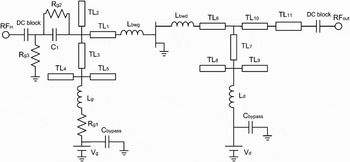
The circuit diagram of the designed inverse class-F PA is depicted in Fig. 5. The space between the bonding pads on the chip and the PCB lines is reduced as much as possible in order to avoid narrow-band and therefore sensitive harmonic matching. L bwg and L bwd are used in the circuit design to model the input and output bondwire inductances, respectively. Their values are estimated to 0.15 nH.
Circuit topology of the PA.

The input matching network consists of transmission lines TLi; i = 1…5, which are optimized to provide, at the input of the device, the optimum impedances obtained from the source/load pull simulations, see Fig. 3.
The input matching network has been slightly modified in order to stabilize the PA. The Rollet stability factor (k) of the amplifier can be improved by increasing the real part of Z 11 [Reference Rollett21]:

A 39 Ω series resistance R g2 is therefore added at the input of the amplifier to improve the stability in the high-frequency band. Further improvement in the amplifier stability in the low-frequency band can be achieved by reducing the low-frequency gain. The parallel resistance R g3, set to 400 Ω, increases low-frequency stability by reducing the input impedance.
The output matching network consists of transmission lines TLi; i = 6…11, which provides the optimum fundamental, second and third harmonics load impedances at the output of the device.
The values of the inductors L g and L d are equal to 28 and 8 nH, respectively. They are used to prevent the leakage of RF into the DC supply lines. The circuit was optimized for wideband operation to minimize the impact of mounting and manufacturing tolerances. It is important to note that the original design did not change significantly after the optimization.
Finally, Monte-Carlo simulations have been used to study the impact of components variability and uncertainty on the PA performance. Uncertainties introduced by the manufacturing process and the lumped components have been considered. The Monte-Carlo simulations have shown that the design is robust and not very sensitive to these variations.
IV. IMPLEMENTATION AND MEASUREMENT RESULTS
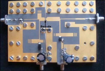
The inverse class-F PA was implemented on a Rogers 5870 substrate with εr = 2.33 and thickness of 0.8 mm. Figure 6 shows a picture of the fabricated inverse class-F amplifier using the bare-die GaN HEMT device.
Fabricated inverse class-F PA. Size: 11 × 8 cm2.

The implemented PA has been characterized by large signal and modulated measurements to study its performance.
A) Large signal measurements
All measurements were made using a continuous wave input signal generated by an Agilent E4438C microwave synthesized source boosted by a microwave driver amplifier and the relevant power levels were measured by a power meter (Agilent E4419B). A low-pass filter with cut-off frequency of 6 GHz has been added at the output of the PA to filter out the power at the harmonics. Hence, only the power at the fundamental frequency have been measured and used in evaluating the PA performance.
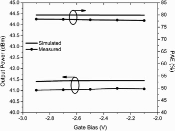
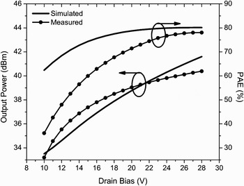
First the bias sensitivity was investigated by a gate bias, V GS sweep. Figure 7 shows simulated and measured output power, P out, and PAE versus V GS. The measurements show that the performance of the PA is not very sensitive to the gate voltage. Results of the drain voltage, V DS, sweep using 29 dBm input power are shown in Fig. 8. It can be noticed that the output power can be further increased by increasing V DS. The measured results agree well with simulations when the input drive level is high enough. From Figs 7 and 8 we conclude that the optimum bias for the PA is V DS = 28 V and V GS = −2.5 V.
Simulated and measured output power and PAE versus gate bias.

Simulated and measured output power and PAE versus drain bias.

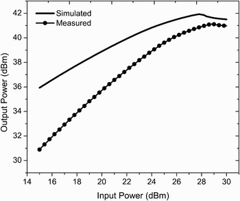
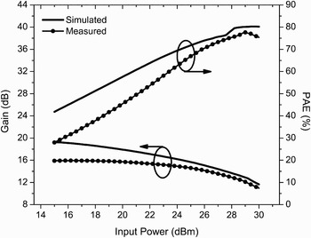
A power sweep measurement has been performed at 3.5 GHz. The simulated and measured output powers versus input power are shown in Fig. 9. As expected, good agreement between simulation and measurement results is obtained at high power levels, where the transistor is operated in a high-efficiency mode that the model was optimized for. The peak power level at the output of this amplifier is about 41 dBm or 12 W. Figure 10 shows the simulated and measured gain and PAE versus input power. A peak PAE of 78% is measured for an input drive level of 29 dBm. There is a good agreement between the simulated and measured results close to the peak efficiency operation.
Simulated and measured output power versus input power.

Simulated and measured PAE and gain versus input power level.

The poor agreement between simulations and measurements at low input powers in Figs 9 and 10 is due to the fact that as the input power is reduced and the device is less overdriven, the harmonic contents of its output waveforms are no longer strong enough to be able to form high-efficiency switching conditions. Therefore, the device operation extends outside of the region where the model is optimized and the simulation results start to deviate from measurements. This is a fact that the PA designer should be aware of. The model is mainly optimized for switched mode or harmonically tuned overdriven operations where conventional models lack accuracy and fail to provide convergence in simulations.
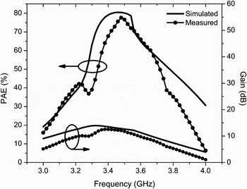
The PA has been characterized versus frequency from 3 to 4 GHz, with a 29 dBm fixed input power drive level. The PAE and gain of the PA are plotted in Fig. 11 and compared with simulations. A good agreement between simulation and measurements is observed at the PA operation frequency. A maximum gain and PAE of 12 dB and 78%, respectively, are located at 3.5 GHz corresponding to a drain efficiency of 82% at this frequency. The amplifier exhibits higher than 50% PAE between 3.32 and 3.72 GHz, which corresponds to greater than 10% fractional bandwidth.
Simulated and measured PAE and gain versus frequency for 29 dBm input power.

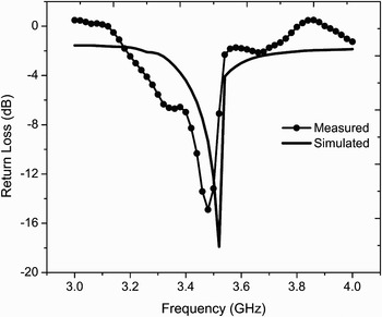
Input return loss have finally been measured under large signal conditions using 29 dBm input power, in the frequency band 3 –4 GHz. Simulated and measured input return loss are shown in Fig. 12, a return loss of 14 dB is obtained at 3.5 GHz and agrees well with simulations.
Simulated and measured large-signal input return loss.

B) Modulated measurements
Modulated measurements are used to evaluate the performance of the PA and show that the PA is linearizable to meet modern wireless communication system standards. In the experiment, a 20 MHz long-term evolution (LTE) signal with 11.2 dB peak-to-average ratio (PAR) and a 5 MHz WCDMA signal with 6.6 dB PAR are used. A relatively low average efficiency is expected when such signals with high PAR are used since the PA has to operate at large back-off most of the time.
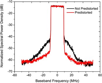
The digital-predistortion (DPD) used, for both LTE and WCDMA signals, is the memory polynomial model with nonlinear 11 and memory depth 5 [Reference Kim and Konstantinou22]. The measured output spectrum at 3.5 GHz of the LTE signal, before and after DPD for an average input power of 18 dBm, is shown in Fig. 13.
PA output signal spectrum of a 20 MHz LTE signal at center frequency of 3.5 GHz before and after DPD.

The adjacent channel power ratio (ACLR) of the PA without DPD reaches −32 dBc with an average PAE of 35% whereas the ACLR of the PA with the DPD applied reaches −42 dBc at an average PAE of 30%.
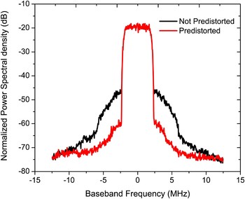
Figure 14 shows the measured output spectrum at 3.5 GHz of the WCDMA signal before and after DPD. In this measurement the average input power used is 19.4 dBm, so the PA was operating at 9.6 dB back-off. When the DPD is applied, the average PAE is decreased from 45 to 40% while 13 dB improvement in ACLR, from −34 to −47 dBc, is obtained.
PA output signal spectrum of a 5 MHz WCDMA signal at center frequency of 3.5 GHz before and after DPD.

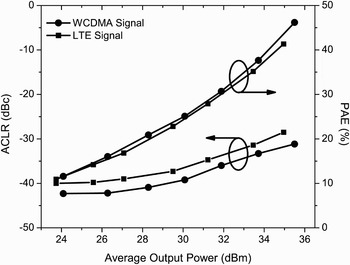
Average PAE and ACLR without DPD for WCDMA and LTE signals are displayed versus average output power in Fig. 15.
PA average performance with a power-swept 20 MHz LTE and 5 MHz WCDMA signals at center frequency of 3.5 GHz.

V. CONCLUSIONS
In this paper, a high-efficiency inverse class-F PA using a GaN HEMT has been presented. The design methodology is based on load-pull/source-pull and harmonic load-pull simulations. A bare-die device, instead of a packaged transistor, is used to minimize the influence of parasitics and therefore take full advantage of recent device technology improvements. The peak PAE of 78% with a power gain of 12 dB was achieved at an output power of 41 dBm at 3.5 GHz. A very broadband performance, with a power gain over 10 dB and PAE over 60%, was maintained over 300 MHz bandwidth. When DPD is used, modulated measurements demonstrate an average PAE of 30% and ACLR of −42 dBc for LTE signal. For WCDMA signal ACLR of −47 dBc and average PAE of 40% were obtained. These results represent state-of-the art for GaN PAs in this frequency range and demonstrate the success of the selected bare-die mounting, modeling, and circuit design methodologies used.
ACKNOWLEDGEMENTS
This research has been carried out in GigaHertz Centre in a joint project financed by the Swedish Governmental Agency for Innovation Systems (VINNOVA), Chalmers University of Technology, ComHeat Microwave AB, Ericsson AB, Infineon Technologies Austria AG, Mitsubishi Electric Corporation, NXP Semiconductors BV, Saab AB, and SP Technical Research Institute of Sweden.
 Paul Saad received the B.S. degree in electrical engineering from the Lebanese University, Beirut, Lebanon, in 2005, the M.S. degree in RF and microwave engineering from university of Gävle, Sweden, in 2007, and is currently working toward the Ph.D. degree at the GigaHertz Centre, Microwave Electronics Laboratory, Chalmers University of Technology. His research concerns the design of high-efficiency and wideband power amplifiers. Mr. Saad was awarded the Certificate of High Achievement of the 2009 Student High Efficiency Power Amplifier Design Competition at the IEEE International Microwave Symposium (IMS).
 Christian Fager received the M.Sc. and Ph.D. degrees in electrical engineering and microwave electronics, from Chalmers University of Technology, Sweden, in 1998 and 2003, respectively. Currently, he is working as a project leader in the GigaHertz Centre at the Microwave Electronics Laboratory. In 2002 he received the Best Student Paper Award at the IEEE International Microwave Symposium. His research interests are in the areas of large signal transistor modeling and high efficiency power amplifier architectures.
 Hossein Mashad Nemati was born in Tehran, Iran, in 1980. He received his B.Sc. degree in telecommunication engineering from Amirkabir University of Technology, Tehran, Iran, in 2004, the M.Sc. degree in microwave electronics from Chalmers University of Technology, Gothenburg, Sweden, in 2006, and is currently working toward the Ph.D. degree at the Microwave Electronics Laboratory, Chalmers University of Technology. His research interests are high-efficiency PAs and transmitter architectures. Mr. Nemati was the recipient of the 2008 Outstanding Achievement Award of the Student High Efficiency Power Amplifier Design Competition of the IEEE Microwave Theory and Techniques Society (IEEE MTT-S) International Microwave Symposium (IMS).
 Haiying Cao received the B.E. degree in communication engineering from Beijing University of Posts and Telecommunications, Beijing, China, in 2005, and the M.Sc. degree in communication engineering from Chalmers University of Technology, Göteborg, Sweden, in 2007. He is currently working toward his Ph.D. degree in Chalmers University of Technology. His research interests include advanced digital signal processing in wireless communication systems, behavioral modeling for RF power amplifiers, and nonlinear system identification algorithms.
 Herbert Zirath received his M.Sc. and Ph.D. degrees from Chalmers University, Gothenburg, Sweden, in 1980 and 1986, respectively. He is since 1996 a Professor in High Speed Electronics at the Department of Microtechnology and Nanoscience, MC2, at Chalmers University. He became the head of the Microwave Electronics Laboratory during 2001. At present he is leading a group of approximately 35 researchers in the area of high frequency semiconductor devices and circuits. His main research interests include foundry-related MMIC designs for millimeterwave applications based on both III–V and silicon devices, SiC- and GaN-based transistors and circuits for high power applications, device modeling including noise and large-signal models for FET and bipolar devices, and InP-HEMT devices and circuits. He is working part-time at Ericsson AB as a microwave circuit expert. He is author/co-author of more than 300 refereed journal/conference papers, and holds four patents.
 Kristoffer Andersson (S'03–M'06) received the M.Sc. and Ph.D. degrees in electrical engineering from Chalmers University of Technology, Göteborg, Sweden, in 2001 and 2006, respectively. His research interests are in the area of characterization and modeling of wide-bandgap transistors.