I. INTRODUCTION
The design and operation of wireless networks nowadays face two main challenges. The first one is the constant proliferation of wireless standards [Reference Simic1] that involve the different stakeholders from base stations and handsets manufacturers, to the final service providers. In the particular case of the base station manufacturers, the demand for co-existence and interoperability of the different standards, imposed by the various specifications, serves to complicate the design, fabrication, and management of the corresponding systems. Using a single radio to cope with multiple standards would address the previously mentioned problems; however, this idea poses a new set of challenges. In fact, radio systems involve a number of frequency-dependent circuits; therefore, multi-standard radio requires multi-band circuits. Among them, the high power amplifiers (PAs) will need to achieve attractive RF performance (gain, output power, and power efficiency) over a range of operating frequencies. Knowing that optimizing these performance metrics at one band is already a challenging task, designing a PA that maintains a high efficiency over a very large frequency bandwidth is another step that can require specific and costly technologies [Reference Colantonio, Giannini, Giofre and Piazzon2, Reference Bespalko and Boumaiza3]. Alternatively, one can target the design of a PA that would maintain a high efficiency over multiple adjacent bands used by a number of standards [Reference Kim, Mkadem and Boumaiza4]. A good example is the 1.805 to 2.17 GHz frequency range that cover three adjacent bands (DCS: 1.805–1.88 GHz, PCS: 1.93–1.99 GHz and Universal Mobile Telecommunications Service (UMTS): 2.11–2.17 GHz) and four standards (Global System for Mobile Telecommunications (GSM), GSM multi-carrier, Wideband Code Division Multiple Access (WCDMA) and Long-Term Evolution (LTE)). In this work, we propose a two-stage LDMOS MMIC PA that can cover the 1.7–2.4 GHz frequency range.
The second challenge is the continuous growth of the consumer demand for data services driven by smart phones, tablets, and other data hungry devices. In fact, some dense urban environments have already run out of capacity causing dropped connections or significant reductions in available data bandwidth. As such, the entire wireless infrastructure ecosystem including operators, original equipment manufacturers (OEM) and component vendors recognize the need to deploy small cells within 3G/4G heterogeneous networks. Operators and equipment vendors will put forth different types of solutions to optimize cell size and coverage based on specific environments and consumer behaviors, but generally operators will support areas of high demand with small cells to offload the macro base-stations thus creating an efficient voice overlay and data underlay. Therefore, the cellular industry will need to solve some challenges including frequency planning, network deployment, management and maintenance, backhaul, and siting. These high-level challenges can, to an appreciable degree, be translated into requirements at the component level including control of output spectrum (RF power and ACLR), low power consumption and dissipation (high efficiency enabling low cost enclosures and Power over Ethernet), small form factor, low weight and low volume, and long-term reliability (minimize in-field failures). To address these challenges, we propose a compact two-stage asymmetric Doherty MMIC (an industry first), that is based on the multi-band MMIC discussed above. In this specific case, although the MMIC has a multi-band capability, the Doherty test board has been specifically tuned for a single communication band (UMTS) in order to demonstrate optimum performance.
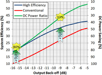
To describe the proposed solutions for both challenges, we will first discuss in Section II some important considerations when designing the wideband 20 W output pre-matched MMIC. Then, we will show in Section III the measured performance in a 50 Ω environment, proving the multi-band capability of this PA. In Section IV, we will use this 20 W MMIC combined with a 40 W counterpart in a dual-path package and provide the performance obtained in an asymmetric Doherty configuration (DPA) for the UMTS band. Finally, in Section V, we will show how the DPA has been optimized in conjunction with a novel pre-distortion technique to enable 33–80% energy saving compared to a conventional solution.
II. WIDEBAND DESIGN
A) Device technology
The technology that has been used to design this amplifier is one of the latest generation of silicon LDMOS. It is a mature, robust, cost-efficient, and continuously improving technology [5], which still largely dominates power amplification for base stations.
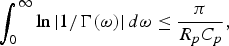
To judge about its wideband capability, the Bode–Fano relation [Reference Pozzar6] can be used. It is a fundamental limitation that governs the ability to match the output of a transistor. Assuming the device output impedance is in form of a parallel RC (R p and C p), the Bode–Fano relation states that
 $$\int_0^\infty {\ln \left\vert {1/\Gamma \lpar \omega \rpar } \right\vert d\omega \leq \displaystyle{\pi \over {{R_p}{C_p}}}}\comma \;$$
where Γ(ω) is the reflection coefficient that can be achieved as a function of frequency. Assuming that the reflection coefficient is constant over the design band (B ω) and unity elsewhere, the integral can be evaluated and the resulting equation solved for the bandwidth:
 $${B_\omega } \leq \displaystyle{1 \over {2{R_p}{C_p}\ln \left\vert {1/\Gamma } \right\vert }}=\displaystyle{{4.343} \over {{R_p}{C_p}RL\lpar dB\rpar }}.$$
The maximum efficiency load for a LDMOS FET device operated at 28 V bias is approximately R p = 280 Ω-mm and C p = 0.3 pF/mm. Matching for an RL(dB) = 20 dB return loss produces a Bode–Fano limited bandwidth of approximately 2.6 GHz. This number is to be compared to the GaN technology where the Bode–Fano limited bandwidth is about 6 GHz [Reference Campbell, Balistreri, Khao, Dumka and Hitt7] or more than two times higher. As a result, LDMOS is clearly not the most performing technology for wideband applications, but considering the above discussed advantages, there are still great interests to continue push it to its limit for using it.
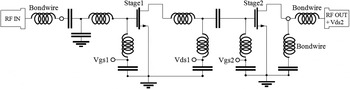
The proposed integrated circuit is made of two amplification stages, whose input and inter-stage matching networks are integrated on die, according to the schematic representation of Fig. 1. The silicon substrate that is used for LDMOS has low resistivity, typically 10 mΩ-mm. As a result, the coupling effects between the metal transmission lines and the substrate lead to important insertion losses. It is therefore mandatory to use adequate design techniques to minimize the effect of these losses. For the same reasons, the output matching is only partially integrated on die: it consists in a band-stop filter realized with bond wires and an integrated shunt capacitor. Indeed, important losses on the load side would have disastrous effects on critical parameters such as efficiency and output power.
Electrical schematic for the 20 W MMIC.

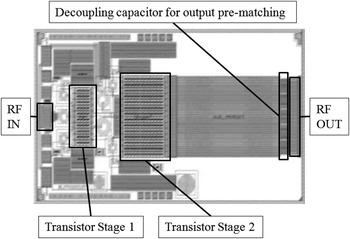
The resulted die layout is then depicted in Fig. 2. To help for the comprehension, the RF input and output pads, the transistors of the two stages and the output decoupling capacitor are labeled.
Die layout of the 20 W MMIC.

B) Design considerations
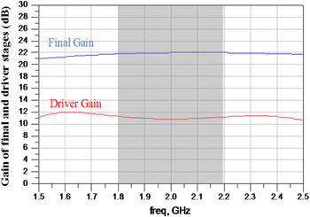
One important criterion to take into account when designing wideband linear PA is to make sure that the targeted bandwidth can be covered entirely by each individual stage. If only partial bandwidth is covered, then there are high risks that the driver stages will go to saturation before the final stages, leading to poor linearity performance.
The simulated gain for each of the two stages of the proposed MMIC is shown in Fig. 3. There is about 1 dB ripple from 1.5 to 2.5 GHz.
Simulated gain of the final and driver stages from 1.5 to 2.5 GHz.

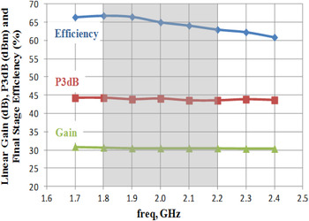
The MMIC PA being only partially output matched, the optimum load impedances need to be determined to reach the best efficiency and power performance. Load-pull measurements were conducted on the packaged MMIC at 28 V drain voltage and a quiescent current of 200 mA corresponding to class AB operation. Resulted optimum performance is shown in Fig. 4.
Load-pull performance measured from 1.7 to 2.4 GHz.

In this figure are represented, as a function of frequency, the linear gain of the two-stage device, the output power at 3 dB compression point (P3 dB) and the peak efficiency of the final stage at the maximum efficiency impedance point. In these measurement conditions, and from 1.7 to 2.4 GHz, the linear gain is higher than 30 dB, the peak efficiency ranges from 61 to 67% and the P3 dB is the vicinity of 44.5 dBm or 28 W. It should be noted that although this MMIC is denominated as a 20 W amplifier, its true peak power capability is significantly greater and can reach up to 37 W (44.7 dBm) when the load is tuned at the maximum output power impedance point.
III. MEASUREMENT RESULTS
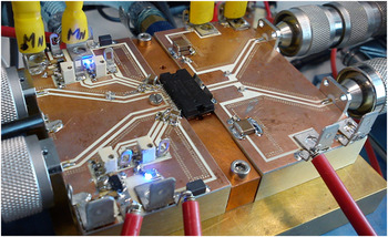
Using the optimum impedances extracted from the load-pull measurements, a test board (Fig. 5) was designed enabling the separate test of two 20 W MMIC blocks assembled in a dual path package. The silicon LDMOS technology is very mature. In addition, as a high-volume industrial assembly process is used, a strong repeatability in the die placement and in the bond wires shaping and positioning can be achieved. As a result, the two paths exhibit very close performance and therefore only the measurements of one path are described.
Photograph of the test board for the dual-path 2 × 20 W MMIC.

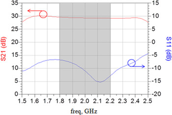
The measurements were performed in class AB operation at 28 V drain voltage. The [S] parameters measurement shows 30 dB of gain from 1.6 to 2.4 GHz with a gain ripple of 0.4 dB (Fig. 6).
[S] parameters measured in a dedicated test board.

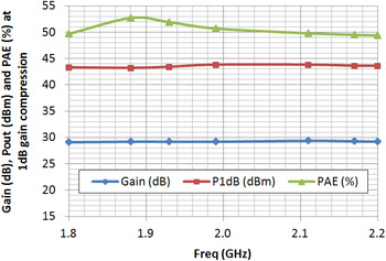
Then, with the device maintained at 25°C temperature thanks to water cooling, Continuous Wave (CW) power measurements have been conducted. They demonstrate 30 dB of maximum gain, 20 W of output power at 1 dB compression and an associated two-stage PAE of 50% from 1.8 to 2.2 GHz (Fig. 7).
CW power performance measured at 1 dB gain compression in a dedicated test board at 28 V drain voltage and in class AB bias conditions.

Another critical parameter for mobile communications is the linearity of the amplifier. This parameter has been verified thanks to the measurements of the adjacent channel power ratio (ACPR) using a single WCDMA carrier with a crest factor of 7.2 dB. The measured value is −43 dBc at 7.5 dB output power back-off.
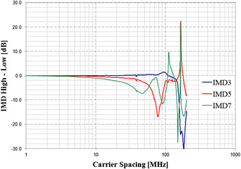
Finally, in addition to the linearity, a VBW (video bandwidth) measurement is necessary to demonstrate the multi-mode capability of the amplifier. The VBW, also called instantaneous bandwidth, represents the ability for an RF PA, to amplify instantaneously a linear signal without asymmetrical distortion. In other terms, it is linked to the broadest modulating signal that can be handled by an RF PA [Reference Bouisse8]. It can be characterized by injecting two CW carriers and logging the output odd order intermodulation (IMD) products versus tone spacing. The frequency at which the third-order resonates is then called the VBW.
Figure 8 shows the resulted difference in between the high and low IMD products of the third, fifth, and seventh order. According to this measurement, the third order IMD resonates at 180 MHz, representing the VBW capability of the device. It is commonly accepted that the VBW needs to be at best two to three times higher than the signal bandwidth for the digital pre-distortion system to be able to correct the amplifier non-linearities. In this case, the measured VBW capability allows the use of 60–90 MHz wide signals.
VBW characterization using two CW carriers.

IV. INDUSTRY FIRST TWO-STAGE ASYMMETRIC MMIC FOR SMALL CELLS
The challenge in the design of small cells is to integrate a complete base station into a small form factor. A key enabler in meeting this goal is high system efficiency. With higher efficiency, the size, weight, and cost of components, heat sinks, power supplies, and enclosures can be reduced.
To address the efficiency requirements of PAs for up to 5 W small cells, several options can be considered. The first option is to use a limited efficiency standard class AB bias and in return, release the constraints on the linearization schemes (no pre-distortion or a simple memory-less one). The second option is to use a high-efficiency amplifier architecture (such as Doherty) in combination with the required adaptive closed-loop linearizer. A quick calculation clearly shows the benefits of the Doherty approach even taking into account the added power consumption associated with the linearizer. Indeed, in the case of a 5 W small cell, the final amplifier has to deliver 10 W of output power in order to offset the 3 dB loss induced by the isolator and filters between the PA output and the antenna. Then, taking the typical assumption of 40% back-off drain efficiency in case of Doherty and 25% in case of class AB, the resulted DC power consumptions are 25 and 40 W, respectively. Hence, a power advantage of 15 W for Doherty. Knowing that DC power consumptions of linearization schemes are in the 5 W range or less, the important energy saving brought by the Doherty architecture completely justifies its use for small cells in the 5 W power range.
To further leverage on this efficiency advantage, more complex architectures such as asymmetric or N-way Doherty are very compelling as they allow another step in efficiency improvement, in particular for peak-to-average ratio (PAR) conditions >6 dB. Among them, the asymmetric Doherty is especially suited for small cells, as the boost in efficiency is obtained within a reduced real estate and cost, since, as for symmetric Doherty, no more than two devices in parallel are necessary. Further improvement in size and cost can be brought when porting this asymmetric Doherty architecture in an integrated circuit technology, as multi-stages can then be embedded in a compact size and in a single package.
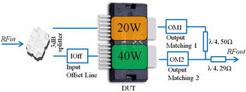
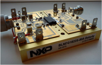
As a result, using an asymmetric Doherty architecture [Reference Doherty9, Reference Colantonio, Giannini, Giofrè and Piazzon10] in conjunction with a multi-stage integrated circuit technology is especially well suited for small cells, as it simultaneously addresses the critical requirements of high efficiency, small size, and low cost. To that end, the 20-W MMIC has been combined with an incremental 40 W MMIC in a dual-path overmolded plastic package and combined in a Doherty topology in a dedicated test board (Fig. 9 and Fig. 10).
Simplified schematic for the asymmetric Doherty MMIC.

Photograph of the test board for the asymmetric Doherty MMIC.

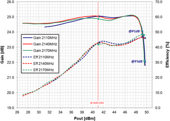
To demonstrate optimum performance, the Doherty test board has been specifically tuned for a single communication band. We will show the results for the more challenging UMTS band (2.11–2.17 GHz). Similar test boards have also been designed for DCS and PCS bands, using the same MMIC device, and have demonstrated at least as good performance. The resulted performance achieved in the UMTS band is shown in the figure below (Fig. 11), representing the gain and efficiency responses versus output power.
Pulsed CW gain and efficiency versus output power.

These measurements have been performed with air-cooling and a pulsed CW signal. Pulse widths of 100 µs and periods of 1 ms are used, which result in a 10% duty cycle. The reason to use a pulsed CW signal is twofold. First, due to the duty cycle of 10%, the thermal effects are minimized. Second, the load-pull data were gathered using pulsed CW signals. Measuring the device using pulsed CW allows an easier comparison of the test board and the load-pull data.
As far as the bias test conditions are concerned: the drain voltage is 28 V, the quiescent currents for the 20 W MMIC main amplifiers are 40 mA for the first stage and 110 mA for the second stage, the gate voltages for the peaking amplifier is 1.7 V for the first stage and 1.55 V for the second stage. Since the peaking amplifier is biased in class C, no quiescent current is drawn.
This plot indicates that the output power at 3 dB compression point is 49.5 dBm (90 W). At 8 dB output back-off (41.5 dBm), the efficiency ranges from 42 to 44% in the UMTS band with an associated gain of 25 dB.
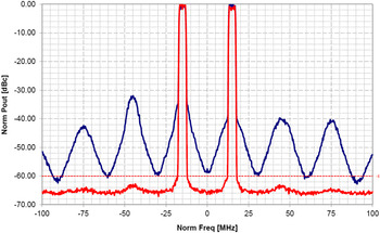
This Doherty amplifier has then been linearized with a digital pre-distortion system that is commercially available (Broadcom 6100 DPD). At central frequency (2.14 GHz) and nominal output power (41.5 dBm), the corrected ACPRs are better than −60 dBc (Fig. 12) using two WCDMA carriers of 35 MHz bandwidth and 7.5 dB of PAR.
Wideband spectrum response before and after DPD.

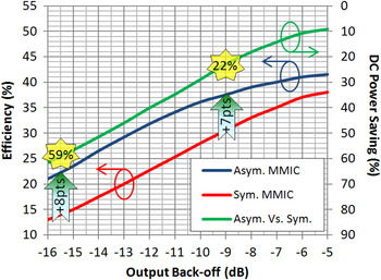
To the authors' knowledge, it is the first time an asymmetric Doherty amplifier based on multi-stage MMIC blocks is demonstrated. To quantify the efficiency boost brought by the asymmetric Doherty architecture, a comparison has been made with a conventional symmetric device (NXP BLM7G22S-60PBG) of the same power range (Fig. 13). The back-off condition to consider drawing this comparison will vary depending on the small cells manufacturer and the level of Crest Factor Reduction (CFR) that is used. Typically a moderately crest factor reduced LTE signal will exhibit 8 dB of PAPR at 0.01% CCDF (versus 10 dB without CFR) that in return will not degrade considerably the EVM (CFR trade-off between EVM and PAR). In the case of a 5 W small cell and using this LTE signal, base station manufacturers will require an 80-W peak device, so that it allows 9 dB of PAR back-off for a 10 W average use case at the output of the PA (or 5 W antenna). This 9 dB back-off condition allows for 1 dB production and temperature margin compared to the signal PAPR. In this case, at the maximum delivered power, the asymmetric configuration will allow 7 points of efficiency boost, leading to 22% saving in power consumption, compared to a conventional symmetric MMIC implementation. This energy saving is even further boosted to 59% at 15.5 dB back-off, corresponding to the point of operation of the small cell under less stringent traffic conditions.
Comparison of asymmetric versus symmetric Doherty efficiencies and DC power saving.

V. HIGH SYSTEM EFFICIENCY FOR SMALL CELLS
The DPA has been specifically designed to deliver best performance with an RF PA Linearizer (RFPAL) from Scintera. It is a predistortion solution optimized for output power levels from 500 mW (RMS) to 80 W (RMS) and amplifier topologies including Class A/AB, and symmetric and asymmetric Doherty. By shifting complex signal processing from the digital domain into the more computationally efficient analog RF domain [Reference Roger11], the RFPAL can achieve low power consumption (typically 200 mW) and high linearization performance, enabling the use of Doherty amplifiers even in small cell applications. The RFPAL is fully adaptive and measures the feedback signal from the PA output to optimize the correction function that is injected at the input of the PA in order to achieve minimum distortion.
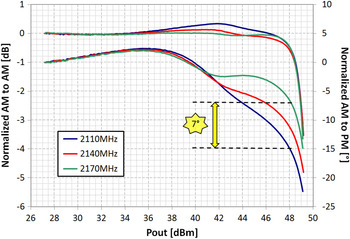
In order to enable best performance when used in conjunction with the RFPAL, focus has been put in meeting three critical requirements allowing optimum pre-distortability for the asymmetric MMIC. First, ACLRs responses are monotonic and do not degrade as the output power decreases. Second, the VBW resonance happens at 80 MHz, in line with a signal bandwidth requirement of up to 40 MHz. Finally, The AM/AM and AM/PM responses are smooth, devoid of rapid slope changes. The maximum relative phase dispersion across the UMTS band is 7° and the 3 dB phase compression is lower than 25° (Fig. 14).
Smooth AM/AM and AM/PM shapes for best results with analog pre-distortion.

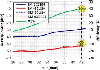
As a result, the amplifier could be effectively linearized by the RFPAL to optimum levels for small cells specific applications. Indeed, small cells manufacturers usually require corrected ACLRs values of −50 dBc, accounting for 5 dB margin against the 3GPP standard specification of −45 dBc. In our case, the −50 dBc corrected ACLRs level could be reached up to the maximum possible output power, corresponding to the 3 dB compressed output power of the amplifier subtracted by the input PAR of the signal. Fig. 15 is illustrating this point using a two-carrier WCDMA signal of 10 MHz bandwidth with 7 dB of PAR. In this case, the maximum linearized output power is 42 dBm (49 dBm − 7 dB), where the amplifier efficiency tops 40%.
40% Efficiency at −50 dBc corrected ACPRs.

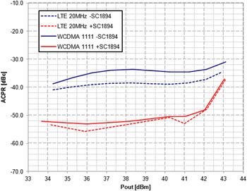
Wider band signals such as four adjacent WCDMA carriers (WCDMA 1111) or LTE 20 MHz, with respective PAR of 7.8 and 7.5 dB at 0.01% CCDF have also been tested. In these cases, ACPRs could be linearized to −50 dBc up to 41 and 41.5 dBm, respectively, in line with the maximum power capability of the MMIC device (Fig. 16).
LTE 20 MHz and WCDMA 1111 ACPRs versus Pout.

When looking at system efficiency and comparing this solution to a conventional DPD and symmetric MMIC implementation, the saving of power consumption is 33% at the maximum operating power of the small cell and as much as 80% at the point where less stringent traffic conditions occur (Fig. 17).
33–80% Energy saving with the novel approach.

VI. CONCLUSION
The need for multi-band multi-mode amplifiers associated to low-cost and compact size constraints has led to the design of a LDMOS MMIC PA covering three adjacent bands from 1.805 to 2.17 GHz. It demonstrates an output power of 20 W at 1 dB compression, 30 dB of gain and 50% of power added efficiency. The multi-mode capability of this amplifier has been proven thanks to the combination of the linearity (−43 dBc at 7.5 dB back-off) and VBW (180 MHz) performance. A Doherty amplifier has then been realized using the 20 W MMIC in combination with a 40 W MMIC in a dual path package, resulting for the first time in an asymmetric MMIC and allowing unprecedented MMIC Doherty performance illustrated in an efficiency result of up to 44% at 8 dB back-off. Finally, being specifically optimized to be used in conjunction with a new pre-distortion solution, the DPA allows 33–80% energy saving at a system level, paving the way for effective deployments of small cells by network operators.
 Xavier Moronval is a principal engineer for the RF Power Business Line at NXP Semiconductors in Toulouse, France. He joined the company in 2011 and has more than 16 years of RF engineering experience during which he held various positions as a design and applications engineer. He has authored 10 articles and holds five patents, awarded and pending. His current interests include wideband high efficiency integrated circuits for base station applications.
 Reza Abdoelgafoer has over 16 years of experience and has worked with the major players in mobile phone and network industry. His expertise spans the whole development chain from mechanical to firmware & software, digital, and analog/RF design. For the last 7 years he has been the interface between the designer and the customer, translating NXP RF-power products to user-friendly applications.
 Adeline Déchansiaud was born in Châteauroux, France, in 1985. She received a Master Professional degree in 2008 from the University of Limoges, and the Ph.D. degree at XLIM laboratory (Limoges University) in June 2012. Her Ph.D. deals with the modeling, the characterization, and the design of an integrated cascode cell to reduce the area of Ku-band amplifiers. She joined NXP in July 2012 as a design engineer on the RF power business line. She is working on characterization/design of MMIC amplifiers for base station applications.