Introduction
A growing number of in situ electron microscopy nanomechanics investigations now rely on microelectromechanical systems (MEMS), from instrumented, active MEMS devices, arrays of passive MEMS structures, or passive “push-to-pull” (PTP) MEMS combined with a nanoindentation transmission electron microscope (TEM) holder.Reference Dehm, Jaya, Raghavan and Kirchlechner1–Reference Zhu and Chang9 These MEMS setups are ideal experimental platforms to simultaneously quantify mechanical properties and to characterize microstructure evolution at the nanometer scale. They can be supplemented and enriched with atomistic models to provide thorough understanding of defect mechanics.Reference Kacher, Zhu, Pierron and Spearot10–Reference Ramachandramoorthy, Wang, Aghaei, Richter, Cai and Espinosa13 So far, most of these studies have focused on elastic and plastic deformation under simple monotonic loadings.
This article provides an overview of current efforts to perform in situ advanced nanomechanical tests for fracture, fatigue, wear, and other properties using integrated micro-/nanofabrication. With these setups, a thorough nanoscale understanding of defect mechanics under complex loading modes (e.g., cyclic, high strain rates, multiaxial), in highly localized regions (i.e., shear instabilities, crack tip, sample surface), and in various reactive environments is now within reach.
In situ tensile tests
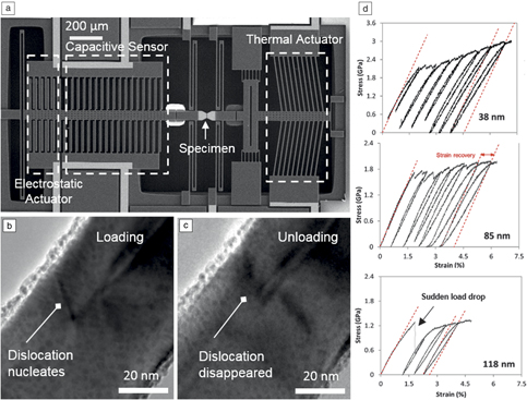
In situ electron microscopy mechanical and electromechanical testing of materials based on MEMS devices, such as the one shown in Figure 1a, has been a powerful approach to unambiguously establish structure–property relationships in low-dimensional metallic and semiconducting materials.Reference Espinosa, Bernal and Filleter2,Reference Ramachandramoorthy, Bernal and Espinosa7 By integrating microscale electronic actuation (with nanometer resolution) and load sensing (with nN resolution), simultaneous acquisition of high-resolution images of the atomic structure of tested specimens during the testing was achieved. This enabled direct imaging of deformation and failure processes with unprecedented resolution.Reference Filleter, Bernal, Li and Espinosa14 For instance, the first direct correlation between failure stress and number of failed shells in multiwalled carbon nanotubes was obtained, which resolved literature discrepancies between theoretical quantum mechanical predictions and experimental measurements of Young’s modulus and strength.Reference Peng, Locascio, Zapol, Li, Mielke, Schatz and Espinosa15 Intershell cross-linking effects, as a function of electron radiation dose, were also revealed in the multiwalled carbon nanotubes.Reference Filleter, Bernal, Li and Espinosa14,Reference Peng, Locascio, Zapol, Li, Mielke, Schatz and Espinosa15
(a) Microelectromechanical systems fabricated on a silicon-on-insulator wafer. (b) Transmission electron microscope image of single dislocation nucleation in pentatwinned silver nanowires. (c) Dislocation glides back and disappears upon unloading (recoverable plasticity mechanism). (d) Stress–strain curves from nanowires of diameters of 38, 85, and 118 nm.Reference Bernal, Aghaei, Lee, Ryu, Sohn, Huang, Cai and Espinosa11

By incorporating feedback control schemes in the MEMS devices, both load and displacement control experiments can be performed. The displacement control tensile testing capability is particularly relevant to nonmonotonic loading, fracture, and adhesion tests. In all of these instances, there is a sudden release of elastic energy stored in the system, which requires stabilization through a feedback controller. In the MEMS device shown in Figure 1a, to achieve a true displacement-controlled test, an electrostatic actuator is implemented within a feedback loop. The voltage output from the load sensor is compared to a reference, with the difference (error) fed to a controller, which sends a compensatory voltage to the electrostatic actuator.Reference Pantano, Bernal, Pagnotta and Espinosa16 The voltage in the electrostatic actuator is then transformed to a force exerted on the load sensor keeping it quasi-stationary (Figure 1a). The elongation and strain of the specimen are calculated from the applied voltage in the thermal actuator using a precalibrated voltage-displacement table.
For simultaneous high-resolution (HR) TEM imaging, the MEMS device is mounted in a customized TEM sample holder.Reference Bernal, Ramachandramoorthy and Espinosa17 An example of such testing is the nonmonotonic testing of silver pentatwinned metallic nanowires in which direct observation of dislocation nucleation and identification of a recoverable plasticity mechanism, arising from dislocation–surface interactions, became possibleReference Bernal, Aghaei, Lee, Ryu, Sohn, Huang, Cai and Espinosa11 (Figure 1b–c). Examination of stress–strain curves obtained from nanowires of various diameters (Figure 1d) revealed not only a size-dependent yield stress, but also an unusually strong Bauschinger effect (i.e., asymmetric plastic flow; in this particular instance, the effect is strong as plastic flow occurs upon unloading from a tensile load).Reference Bernal, Aghaei, Lee, Ryu, Sohn, Huang, Cai and Espinosa11 Likewise, by exploiting the testing stability afforded by feedback control, the mechanical reliability of single-crystal silver nanowire-based systems was ascertained by identifying time-dependent stress-assisted atomic diffusion mechanisms, over several hours, leading to necking instabilities.Reference Ramachandramoorthy, Wang, Aghaei, Richter, Cai and Espinosa13 Remarkably, such a nonmonotonic deformation process is particularly relevant to emerging applications using transparent electrodes based on silver nanowire networks, such as flexible electronic sensors, solar cells, and touch screens.Reference Sannicolo, Lagrange, Cabos, Celle, Simonato and Bellet18
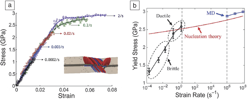
Characterization of thin films and low-dimensional materials, as a function of strain rate, is another tensile testing mode of interest that goes beyond typical stress and strain measurements. The low mass of microsystems combined with electronic actuation and sensing enables the exploration of rate effects.Reference Ramachandramoorthy, Gao, Bernal and Espinosa12,Reference Ramachandramoorthy, Milan, Lin, Trolier-McKinstry, Corigliano and Espinosa19 By employing such testing capability, bicrystalline silver nanowires were tested in tension under a range of strain rates. A brittle-to-ductile transition was revealed at a strain rate of ∼1/s (Figure 2a).Reference Ramachandramoorthy, Gao, Bernal and Espinosa12 To gain insight into the mechanism responsible for such transition, a comparison to a theoretical-atomistic model of the experiment was pursued (Figure 2b). It was ascertained that measured yield stresses were consistent with a dislocation nucleation-controlled strain-rate-dependent model.Reference Ramachandramoorthy, Gao, Bernal and Espinosa12,Reference Zhu, Li, Samanta, Leach and Gall20 The model includes an activation volume term, a quantity characterizing the governing thermally activated dislocation mechanism. Such an activation volume can be computed numericallyReference Ramachandramoorthy, Gao, Bernal and Espinosa12,Reference Zhu, Li, Samanta, Leach and Gall20 or determined experimentally. For the latter, a MEMS device consisting of two capacitive sensors on each side of the specimen, providing accurate measurements of stress and plastic strain, was recently used.Reference Hosseinian, Legros and Pierron21–Reference Gupta and Pierron23 This MEMS device enables miniaturized transient tests such as repeated stress relaxation tests, and therefore simultaneous measurement of true activation volume and TEM observations of the governing mechanisms.
(a) Brittle-to-ductile transition as a function of strain rate in silver nanowires. Inset shows snapshot from molecular dynamics (MD) simulation at a strain rate of 106/s.Reference Ramachandramoorthy, Gao, Bernal and Espinosa12 (b) Comparison of measured yield stress and molecular dynamics predictions via nucleation theory.

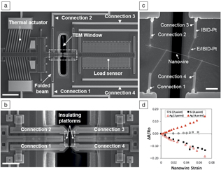
Investigation of coupled fields is another area in which MEMS devices find natural application. Coupled fields, such as piezo-resistivity and piezo-electricity, are of high relevance to emergent nanotechnologies based on low-dimensional freestanding materials. It is known that when two-point measurements are performed, spurious size effects can result from the added contact resistance. Hence, novel MEMS that allow integrated four-point, uniaxial, electromechanical measurements of freestanding nanostructures in situ electron microscopy are needed. One implementation is built on the thermal actuation-capacitive load measurement architecture.Reference Bernal, Filleter, Connell, Sohn, Huang, Lauhon and Espinosa24 Specifically, as shown in Figure 3a, four electrical traces coming from outside electronics are connected by anchors and vias to compliant, conductive folded beams that allow electrical access to the moving shuttles where the nanowire specimen is positioned. The folded beams are then interfaced with interconnects, which are brought to the vicinity of the specimen (Figure 3b). The folded beams and interconnects are fabricated from highly doped polysilicon. In order to ensure that all four electrical signals are independent from each other, an insulating freestanding silicon nitride layer is deposited in the fabrication process. To complete the electrical connections to the specimen, ion- or electron-beam-induced platinum deposition (IBID-Pt or EBID-Pt) is used to pattern connections from the polysilicon interconnects to the specimen (Figure 3c). By employing such a MEMS device, the piezo-resistivity of silver nanowires and n-type [111] silicon nanowires, up to unprecedented strain levels (>7%), was quantified (Figure 3d).Reference Bernal, Filleter, Connell, Sohn, Huang, Lauhon and Espinosa24
(a) Microelectromechanical systems for four-point electromechanical measurements. Scale bar = 200 μm. (b) Image of shuttles in the specimen region and configuration of interconnects. Scale bar = 40 μm. (c) Details of mounted nanowire specimen and traces of electron-/ion-beam-induced deposition of platinum. Scale bar = 4 μm. (d) Two- and four-point resistivity measurements as a function of strain for silver and silicon nanowires.Reference Bernal, Filleter, Connell, Sohn, Huang, Lauhon and Espinosa24 Note: TEM, transmission electron microscope.

In situ fracture tests
The first generation of MEMS mechanical test devices focused on extracting the uniaxial tensile stress–strain response of brittle thin films, allowing the determination of fracture stress σc, and the associated Weibull statistics.Reference van der Rest, Idrissi, Henry, Favache, Schryvers, Proost, Raskin, Van Overmeere and Pardoen25,Reference Passi, Bhaskar, Pardoen, Sodervall, Nilsson, Petersson, Hagberg and Raskin26 Combined with microscopy analysis, the σc distribution provides information on surface or bulk defects controlling cracking initiation and the inter- versus transgranular propagation mechanisms for crystalline systems. Fracture toughness can be inferred from these tests based on the estimated defect size or vice versa.Reference Yagnamurthy, Boyce and Chasiotis27 Nevertheless, true fracture mechanics tests are preferable to more directly (and accurately) quantify fracture toughness, K c. Hence, further developments were aimed at testing precracked fracture mechanics specimens to evaluate the fracture toughness as well as to stabilize the failure process and facilitate in situ TEM analysis of the damage and fracture mechanisms.Reference Zhang, Ma, Fan, Zeng, Peng, Loya, Liu, Gong, Zhang, Zhang, Ajayan, Zhu and Lou28 In brittle films, the plastic zone size is in the nanometer scale, which warrants valid K c measurements.
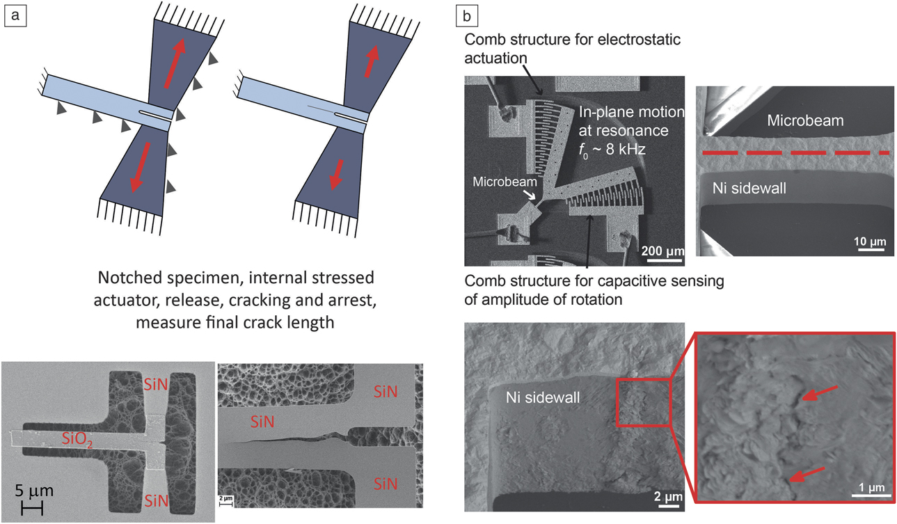
One difficulty is that extremely sharp precracks are needed for valid measurements, therefore, caution should be taken with focused ion beam precracking.Reference Dehm, Jaya, Raghavan and Kirchlechner1 Precracking by the crack arrest method is the most suitable approach.Reference Hatty, Kahn and Heuer29 Recently, a MEMS structure (Figure 4a) actuated by internal stress has been developed with a stable cracking configuration.Reference Jaddi, Coulombier, Raskin and Pardoen30 A crack is initiated from a notch, propagates and arrests due to a geometrically dictated decrease in K. The fracture toughness is determined from the final crack length after release of the test structure. The technique has been successfully applied to freestanding silicon nitride films. In situ HRTEM analysis near the cleavage crack tip region under loading has the potential to provide new insights into the fundamental cracking mechanisms.
(a) Top shows schematic and bottom shows scanning electron microscope (SEM) images of a microelectromechanical systems-type fracture mechanics test: cracking is induced from a notch, the loading comes from internally stressed actuator beams, and the fracture toughness is measured from the arrest crack length. (b) (Top) SEM image of a Ni microresonator with an inclined magnification image of the microbeam. (Bottom) Inclined SEM images of a microbeam after in situ SEM fatigue test (σa = 440 MPa, fatigue life: 8.1 × 10⁷ cycles).Reference Barrios, Gupta, Castelluccio and Pierron39

The fracture resistance of ductile films is quantified by the fracture strain εf, which is stress-state dependent, or by K c.Reference Pineau, Benzerga and Pardoen31 Fracture strain in a variety of ductile films has been measured by MEMS test devices.Reference de Boer, Corwin, Kotula, Baker, Michael, Subhash and Shaw32,Reference Jonnalagadda, Karanjgaokar, Chasiotis, Chee and Peroulis33 Similar to brittle films, the determination of K c faces the problem of precracking.Reference Dehm, Jaya, Raghavan and Kirchlechner1 Crack arrest measurement from a notch using a MEMS structure is an option.Reference Jaddi, Coulombier, Raskin and Pardoen30 For these tests, K c corresponds to the near plane stress regime and is thickness dependent.Reference Hosokawa, Desai and Haque34,Reference Lanning, Javaid and Muhlstein35 Nevertheless, the main merit of MEMS structures is to allow, on uncracked or cracked specimens, in situ TEM analysis of the evolution of plastic localization (see previous section), damage and near crack fracture process zone mechanisms under well controlled mechanical conditions.Reference Mompiou, Legros, Boe, Coulombier, Raskin and Pardoen36–Reference Kumar, Alam and Haque38
In situ fatigue tests
Characterizing nanoscale fatigue of metals is a critical research area, to provide a better understanding of small fatigue crack behavior as well as to ensure proper reliability of microcomponents. Metallic MEMS microresonators (Figure 4b) are integrated fatigue testing machines, whereby a microbeam can be cycled at resonance under fully reversed loading conditions at large frequencies (kHz regime).Reference Barrios, Gupta, Castelluccio and Pierron39–Reference Sadeghi-Tohidi and Pierron41 These devices are miniaturized versions of bulk ultrasonic fatigue testing devices, and as such, can be tested inside a SEM.Reference Barrios, Gupta, Castelluccio and Pierron39 The evolution of the measured resonance frequency can be used as a proxy to quantify nanoscale fatigue damage, including ultralow average crack growth rates (down to 10–14 m.cycle–1).Reference Barrios, Gupta, Castelluccio and Pierron39
In situ TEM nanodynamics is a powerful testing technique used in recent instruments to obtain fatigue properties and to observe structural changes during cyclic loading.Reference Kumar, Alam and Haque38,Reference Hosseinian and Pierron42,Reference Bufford, Stauffer, Mook, Asif, Boyce and Hattar43 MEMS-based actuators, sensors, and sample mounts have been used to conduct high frequency in situ TEM fatigue tests. Bufford et al. recently studied tensile fatigue of nanocrystalline Cu films using a PTP MEMS-based sample mounting device inside a TEM.Reference Bufford, Stauffer, Mook, Asif, Boyce and Hattar43 PTP is a passive MEMS device on which one- and two-dimensional (2D) specimen (e.g., nanowires, nanotubes and thin films) can be mounted. The pushing of the flat end of the PTP device with a nanoindentation TEM holder results in the tensile deformation of the specimen.Reference Yu, Legros and Minor8 The high resolution of the TEM enabled observations of structural changes and localized grain growth in front of the crack tip of the Cu film. Using the captured crack growth video, a precise crack extension rate of 6 × 10–12 m•cycle–1 was calculated, which is equivalent to breaking tens of atomic bonds on average during each cycle.
In situ wear testing
Traditional tribology studies are limited by the inability to observe real-time progress of deformation at the sliding interfaces. Recent developments of small-scale devices, particularly piezoelectric and MEMS-based actuators, aid in observing atomic-scale dynamic deformation and understanding the fundamentals of sliding contacts in single asperity wear, superlubricity, biomedical, and magnetic storage. MEMS actuators can provide high force- and displacement-resolution, and good thermal stability, which are important factors for obtaining precise mechanical properties and for capturing high-resolution images during a tribology test.
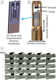
A “2D” MEMS transducer was used recently in in situ cyclic nanofriction experiments on a single WS2 nanoparticle.Reference Jenei and Dassenoy44 Exfoliation of the particle during a sliding event was observed in the TEM, which was correlated to the change in the coefficient of friction. The transducer used in this study (Bruker Nano Surfaces) consists of two electrostatic micromachined comb drives in a single body that actuate and sense force and displacements in normal and lateral directions. A diamond tip is coupled to a comb drive that actuates motion toward the indentation axis, while the second comb drive, comprising a plurality of electrostatic capacitive actuators, drives the same probe perpendicular to the indentation axis.
This MEMS transducer was used in another study to understand the failure mechanism of a perpendicular magnetic recording film stack under scratch loading.Reference Hintsala, Stauffer, Oh and Asif45 The film structure consisted of a 2-nm-thick diamond-like carbon (DLC) protecting two functional layers below (a metallic layer and its stoichiometrically equivalent oxide). These types of films are widely utilized in storage devices and loss of data by grain reorientation in the recording layers is a primary failure mechanism. In situ observation revealed that surface asperities on the DLC coating were removed at low normal force, where grain reorientation and debonding of the columnar metallic and oxide recording layers occurred at high normal force.
A similar multicycle scratch test was run on an olivine specimen and the formation of dislocation plasticity was observed under the indenter tip (Figure 5).Reference Bhowmick, Hintsala, Stauffer and Asif46 Symmetric arrays of defects appeared along the wear path and the number of arrays increased after each pass. The kinetic friction coefficient was determined to be 0.1 and was relatively constant with increasing wear passes. Sato et al. recently integrated two perpendicular MEMS actuators into a single device, then conducted in situ wear tests using two silicon indenters attached to the actuators.Reference Sato, Tochigi, Mizoguchi, Ikuhara and Fujita47 The interaction, deformation, and separation at the nanojunctions of silver nanoparticles were observed in the TEM while the normal and lateral forces were detected during the sliding event in real time.
(a) Two-dimensional (2D) microelectromechanical systems load and displacement sensing transducer for in situ tribological applications, (b) front part of a Hysitron in situ nanomechanical instrument, transmission electron microscope picoindenter showing location of the sample and transducer, and (c) image montage showing gradual defect nucleation during five passes of an in situ scratch test on single-crystal olivine. Scale bars = 100 nm.Reference Bhowmick, Hintsala, Stauffer and Asif46

Outlook: Environmental in situ nanomechanics
The aforementioned in situ nanomechanics techniques are currently mostly limited to vacuum conditions. While a few examples of MEMS in situ techniques operating at high temperaturesReference Zhu and Chang9,Reference Elhebeary and Saif48 or under irradiation conditions exist,Reference Lapouge, Onimus, Coulombier, Raskin, Pardoen and Brechet49,Reference Lapouge, Onimus, Vayrette, Raskin, Pardoen and Brechet50 there is a clear need to extend MEMS platforms for nanomechanical testing beyond the high-vacuum conditions within the TEM in order to study the structure–property relationship at the atomic scale in technology-relevant environments.Reference Ramachandramoorthy, Wang, Aghaei, Richter, Cai and Espinosa13 As such, integrating MEMS platforms with an environmental TEM (ETEM)Reference Boyes and Gai51 could be used to study the mechanical impact from redox environments, corrosive environments, hydrogen embrittlement, and catalytic reactions, all at variable gas compositions and temperatures. However, because the compatibility of the MEMS device with the ETEM imposes modifications to the functionality of the MEMS platform, the exposed regions of the MEMS platform and the electrical contacts must be evaluated for reactivity with the test gas to prevent adverse effects.Reference Gianola, Sedlmayr, Mönig, Volkert, Major, Cyrankowski, Asif, Warren and Kraft52 Though many studies have combined ETEM with quantitative straining holders,Reference Epicier, Joly-Pottuz, Jenei, Stauffer, Dassenoy and Masenelli-Varlot53–Reference Xie, Li, Li, Wang, Gumbsch, Sun, Ma, Li and Shan55 demonstration of a nanomechanics MEMS platform within an ETEM has not been previously published.
Higher pressure gaseous and liquid experiments are generally conducted within the TEM using a hermetically sealed cell. These cells are composed of two silicon nitride (SiN) windows that confine the gaseous or liquid environment within, retaining atomic-scale imaging through the constraint of background scattering caused by the SiN window thickness and the gas/liquid thickness.Reference Jungjohann and Carter56 However, these have not yet been combined with mechanical actuation of the enclosed sample.
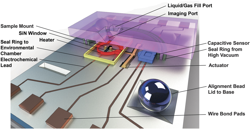
A closed-cell mechanical-environmental-thermal MEMS platform for tensile testing of electron transparent specimens within atmospheric gaseous or liquid environments is being developed,Reference Jungjohann, Mook, Chisholm, Shaw, Hattar, Galambos, Leenheer and Hearne57 which segregates the actuation elements from the static environmental cell using patterned barriers (Figure 6). A barrier piston arm connects the sample (which is set between the SiN windows) to the actuator (which operates under an atmospheric environment). A hydrophobic self-assembled monolayer within the piston arm channel prevents liquid from leaking into the actuator. This platform has the potential to provide the lab-in-a-gap conditions needed to couple multiple modes of in situ control (elevated temperature control and electrochemical contacts) to mechanical tensile testing within the TEM. For example, experiments on the mechanical properties of biological submicron materials may be conducted within this type of cell under physiologically relevant environmental conditions. Additionally, materials problems, such as stress-corrosion-cracking mechanisms and stress-induced electrochemical degradation mechanisms, can be visualized at the atomic-scale during operation of this MEMS device in a TEM.
Mechanical-environmental-thermal microelectromechanical systems (MEMS) platform for transmission electron microscopy testing of atmospheric gaseous or liquid environments with temperature control, electrochemical control, and displacement sensing capability (under development). Lid (pink cross section) and base (gray) are sealed using epoxy to create the static cell. Bond pads (copper) connect the MEMS device to the holder for external control.Reference Jungjohann, Mook, Chisholm, Shaw, Hattar, Galambos, Leenheer and Hearne57

Acknowledgments
This work (K.J. and O.P.) was performed, in part, at the Center for Integrated Nanotechnologies, an Office of Science User Facility operated for the US Department of Energy (DOE) Office of Science. Sandia National Laboratories is a multimission laboratory managed and operated by National Technology and Engineering Solutions of Sandia, LLC, a wholly owned subsidiary of Honeywell International, Inc., for the DOE’s National Nuclear Security Administration under contract DE-NA-0003525. The views expressed in the article do not necessarily represent the views of the DOE or the US Government. H.D.E. gratefully acknowledges support from the National Science Foundation (NSF) through Award Nos. DMR-1408901 and DMREF-CMMI-1235480, ARO through Award Nos. W911NF1510068 and MURI Award No. W911NF-08–1-054. O.P. acknowledges support of the NSF (Award Nos. DMR-1255046 and CMMI-1562499) and DOE-BES (DE-SC0018960).

Sanjit Bhowmick is a senior staff scientist at Bruker Nano, Inc. He received his PhD degree in materials engineering from the Indian Institute of Science, Bangalore, in 2004. He completed postdoctoral research at the National Institute of Standards and Technology. His research interests include in situ transmission electron microscopy and scanning electron microscopy characterization of mechanical properties of small-scale structures and high-temperature properties of materials. He is involved in the development of projects of nanomechanical instruments for electron microscopy (Hysitron’s PicoIndenter products). He has authored or co-authored more than 90 publications. Bhowmick can be reached by email at sanjit.bhowmick@gmail.com.

Horacio D. Espinosa is the James and Nancy Farley Professor of Manufacturing and Entrepreneurship, Professor of Mechanical Engineering, and Director of the Theoretical and Applied Mechanics (TAM) Program at the McCormick School of Engineering and Applied Sciences at Northwestern University. He received his PhD degree in solid mechanics from Brown University in 1992. His research includes the areas of dynamic failure of advanced materials, mechanics of biomaterials, and micro-/nanomechanics. He is a member of the European Academy of Arts and Sciences, the Russian Academy of Engineering, and a Fellow of the AAAS, AAM, the American Society of Mechanical Engineers (ASME), and the Society for Experimental Mechanics (SEM). His awards include the PRAGER Medal from the Society of Engineering Science, the MURRAY and SIA NEMAT-NASSER Medals from the SEM, the ASME THURSTON Award, and the LAZAN and HETENYI Awards from SEM. He serves on the US National Committee on TAM and the IUTAM Congress Committee. Espinosa can be reached by email at espinosa@northwestern.edu.

Katherine Jungjohann is a staff scientist at the Center for Integrated Nanotechnologies (CINT), the thrust leader for the In Situ Characterization and Nanomechanics Thrust at CINT, and the co-leader of the Microscopy Society of America’s Focused Interest Group on Electron Microscopy in Liquids and Gases. Her current research focuses on developing new capabilities for in situ transmission electron microscopy imaging of environmentally relevant materials processes and energy-storage interfaces and corrosion mechanisms. Jungjohann can be reached by email at kljungj@sandia.gov.

Thomas Pardoen is a full professor and president of the Institute of Mechanics, Materials and Civil Engineering at the Université Catholique de Louvain (UC Louvain), Belgium, as well as chairman of the Scientific Council of the Belgian Nuclear Research Center SCK•CEN, Belgium. He received his master’s degrees in engineering and philosophy, and his PhD degree in 1998 at UC Louvain. He completed postdoctoral research at Harvard University. His research focuses on the nano-, micro-, and macromechanics of materials with emphasis on multiscale experimental investigations and modeling of deformation and fracture. He has supervised 45 doctoral candidates and 20 postdoctoral researchers, and has published >200 papers in international journals. He received the 2011 Grand Prix Alcan of the French Academy of Sciences and a 2015 Francqui Chair, and was nominated as a Euromech Fellow in 2015. Pardoen can be reached by email at thomas.pardoen@uclouvain.be.

Olivier Pierron is a professor in the Woodruff School of Mechanical Engineering at the Georgia Institute of Technology. He received his engineering degree from École des Mines de Paris, France, in 2000, and MS and PhD degrees in materials engineering from The Pennsylvania State University, in 2002 and 2005, respectively. He was a senior engineer at Qualcomm MEMS Technologies from 2005 to 2007. His research focuses on the mechanics of materials for micro- and nanoengineering applications. He is the recipient of a 2013 National Science Foundation CAREER Award and the 2014 Hetényi Award. Pierron can be reached by email at olivier.pierron@me.gatech.edu.