Introduction
Advances in pulsed direct current (DC) generators have been made with the aims of preventing arcing and improving film qualities for plasma discharge. To date, the most prominent and highly studied process used in thin-film research is high-power impulse magnetron sputtering (HiPIMS) [Reference Lundin and Sarakinos1, Reference Lin, Moore, Sproul, Mishra, Rees, Wu, Chistyakov and Abraham2, Reference Alami, Gudmundsson, Bohlmark, Birch and Helmersson3, Reference Greczynski and Hultman4]. HiPIMS is a physical vapor deposition (PVD) method for thin films based on magnetron sputter deposition. It utilizes high-power pulsed DC generators that supply extremely high power densities in short pulses of tens of microseconds at low duty cycles. HiPIMS has shown to be effective for high ionization and the ability to adjust pulse output to improve desired film qualities, all at low deposition temperatures. Pulsing dramatically increases the energetics of the plasma by producing ionized atoms with much higher energy levels than conventional sputtering. The high peak power pulses in HIPIMS result in plasma electron densities up to 1016 cm−3, which is three orders of magnitude higher compared with conventional DC magnetron sputtering [Reference Lin, Moore, Sproul, Mishra, Rees, Wu, Chistyakov and Abraham2, Reference Alami, Gudmundsson, Bohlmark, Birch and Helmersson3]. These high plasma densities result in a high degree of ionization of the sputtered target material, where the ionization fraction can reach up to 90% [Reference Greczynski and Hultman4]. In this manner, HiPIMS has become a well-known technology for adhesion enhancement pretreatment and deposition of high-density, high-performance thin films. While the use of high-power pulsed generators is known to be beneficial for low-pressure discharges, their benefits to high-pressure and/or atmospheric pressure discharges are largely unexamined.
Over the past two decades, several nonequilibrium atmospheric-pressure plasma discharge schemes have been developed and characterized, providing so-called ‘cold’ or nonthermal plasmas where the electron temperature is much greater than the ions, neutrals, and gas (T elelctron ≫ T ion ≈ T neutral ≈ T gas) [Reference Schütze, Jeong, Babayan, Park, Selwyn and Hicks5]. Many of these sources produce plasmas that are geometrically confined to the area between the electrodes (e.g., dielectric barrier discharge (DBD)). More recently, nonequilibrium atmospheric pressure plasma jets (APPJs) have been developed with the active area not bound by physical walls. Existing APPJs produce discharge at atmospheric pressure and relatively low gas temperatures and employ a high flow of feedstock gas (e.g., He, Ar, and air), with at times an admixture of molecular gases, so that the plasma rapidly exits the source and impinges downstream on the work piece. APPJs have been developed that use radio frequency (RF), DC, low-frequency alternating current (AC), and microwave power. Several APPJ designs and geometries have been developed, including DBD, microhollow cathode discharges, transferred arcs, and capacitively coupled discharges [Reference Schütze, Jeong, Babayan, Park, Selwyn and Hicks5, Reference Nehra, Kumar and Dwivedi6, Reference Kong, Ganguly and Hicks7, Reference Laroussi and Akan8, Reference Laimer and Störi9]. These systems have expanded the plasma toolkit to allow for ambient temperature and pressure operations. Nonequilibrium APPJs are being examined for a variety of applications, including surface treatments, sterilization, etching, and decontamination, as well as in coating technologies [Reference Schütze, Jeong, Babayan, Park, Selwyn and Hicks5, Reference Nehra, Kumar and Dwivedi6, Reference Kong, Ganguly and Hicks7, Reference Laroussi and Akan8, Reference Laimer and Störi9, Reference Morajev and Hicks10, Reference Yim, Rodriguez-Santiago, Williams, Gougousi, Pappas and Hirvonen11, Reference Jain, Macia-Montero, Velasumy, Maguire and Mariotti12, Reference Dong, Watanabe and Deauskardt13, Reference Sawada, Ogawa and Kogoma14].
Metallic or ceramic coatings are commonly deposited using a vacuum process such as a PVD or plasma-enhanced chemical vapor process (PECVD). PVD of metallic and nitride coatings is an industrially mature technology utilized to deposit hard coatings with high resistance to wear, corrosion, and heat [Reference Navinsěk, Panjan and Milosěv15]. Yet, a vacuum chamber is needed so that plasma can be generated fairly easily at a low gas pressure, typically from a few millitorr to a few hundred torr. Although the coating quality of vacuum-based processes is quite high, depositing coatings using low-pressure processes inside a vacuum system is very cumbersome, time-intensive, and expensive. In addition, for some applications, vacuum deposition is impractical as in treating large and/or complex geometric substrates, such as airplane wings or ship impellers, or nonvacuum compatible substrates, such as biological materials or some polymers. Thus, atmospheric pressure plasmas have gained increasing interest as an alternative method for obtaining similar coatings.
Thermal plasmas (e.g., inductively coupled plasma (ICP), plasma torch, and thermal plasma spray) are existing commercialized methods to deposit metallic or ceramic coatings using plasma at atmospheric pressure. Thermal plasma spray operates in the high-power DC mode to achieve a high flame temperature (6000–11,000 °C) so that the metallic powder can be melted and hence deposited [Reference Pfender16]. The power requirement is typically in the range of a few hundred kilowatts. To minimize the local overheating of the part, samples have to be rotated or moved away quickly from the plasma torch. Because of the high-power DC operation mode, the resultant coating can be quite thick (typically in the range of 0.1–5 mm) and generally porous [Reference Pfender16].
Nonthermal atmospheric pressure plasma is an emerging technique that enables plasma deposition of coatings in ambient air without the need for a vacuum chamber. Recent efforts have focused on the use of nonthermal APPJ systems with gas and liquid-based precursors, such as hydrocarbons, fluorocarbons, silanes, siloxanes, and organometallics, to carry out atmospheric pressure plasma-enhanced chemical vapor deposition or plasma polymerization of variety of materials, including silica [Reference Morajev and Hicks10], organosilicon [Reference Yim, Rodriguez-Santiago, Williams, Gougousi, Pappas and Hirvonen11], metal oxides [Reference Jain, Macia-Montero, Velasumy, Maguire and Mariotti12, Reference Dong, Watanabe and Deauskardt13], nitrides [Reference Dong, Watanabe and Deauskardt13], and polymer coatings [Reference Sawada, Ogawa and Kogoma14].
In this study, a novel high-power impulse plasma source (HiPIPS) technology that combines APPJs with pulsed power modes of excitation is described. The HiPIPS technology is a hybridization of nonthermal atmospheric pressure plasma with high-power pulsed DC generators. Power is applied in microsecond pulses at low duty cycle and low frequency leading to high peak power densities and high peak currents, while maintaining low average power and low processing temperatures. These conditions result in the generation of a highly dense plasma discharge, with increased ionization for surface modification and deposition of coatings. Plasma properties of HiPIPS were characterized by using current–voltage probes, Langmuir probe, and optical emission spectroscopy (OES). HiPIPS was investigated for proof-of-concept deposition of CoCr and Ti–6Al–4V coatings. The microstructure and elemental composition of the resulting coatings were examined with scanning electron microscopy (SEM) and energy-dispersive X-ray spectroscopy (EDS). The hardness was measured using a nanoindentation technique.
Results and discussion
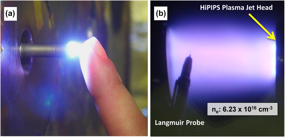
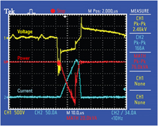
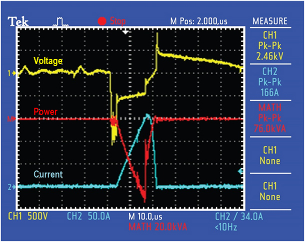
HiPIPS utilizes APPJs with high-power pulsed DC generators that supply extremely high power densities in short pulses of tens of microseconds at low duty cycles. Figure 1(a) is demonstrative of the atmospheric pressure and low-temperature capability of HiPIPS. The development of the HiPIPS plasma source involved experiments where the process parameters were systematically varied to examine their effects on the resulting HiPIPS plasma. HiPIPS investigations with argon gas and Ti, CoCr, and Ti–6Al–4V wires confirmed that high peak power pulses can be achieved (10–70 kW), resulting in high peak currents (100–250 A) and increased ionization and plasma density, while maintaining low average power (40 W) and substrate processing temperatures (<50 °C). Figure 2 shows a snapshot of the voltage, current, and power traces for one pulse of HiPIPS running with Ar gas and a Ti–6Al–4V electrode. The typical high peak currents (166 A) and high peak powers (76 kW) in the pulse can be observed. Other parameters, such as the peak voltage of 2.46 kV, pulse frequency of 500 Hz, and pulse width of 20 µs, can be seen on the oscilloscope readouts. Electron densities measured by the Langmuir probe were 6.23 × 1016 cm−3, equating to a mean electron temperature (kT e) of 27,300 K (2.352 eV) from the end of the HiPIPS plasma source at a pressure of 0.5 torr (67 Pa) [Fig. 1(b)]. Altogether, these HiPIPS investigations revealed that high peak power pulses can be achieved, which result in high peak currents and increased ionization and plasma density, while maintaining low average power and substrate processing temperatures.
Images of the (a) HiPIPS Ar plasma source demonstrating atmospheric, low-temperature capability and (b) Langmuir probe measurement of the HiPIPS Ar plasma source at 0.5 torr (67 Pa).

Voltage, current, and power traces for one pulse of HiPIPS running with Ar gas and a Ti–6Al–4V electrode. High peak currents (166 A) and high peak powers (76 kW) in each pulse, as shown, are typically observed.
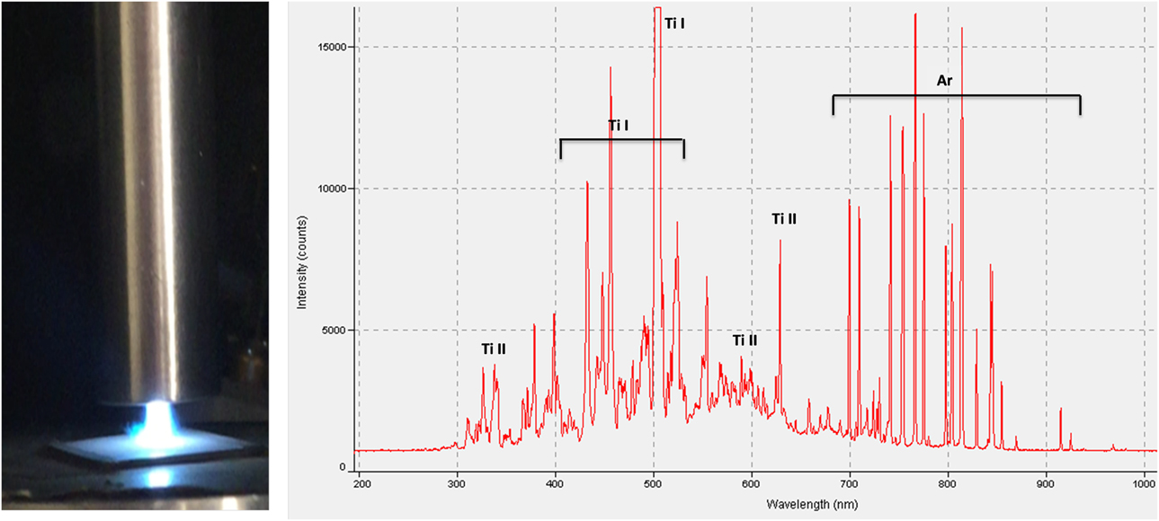
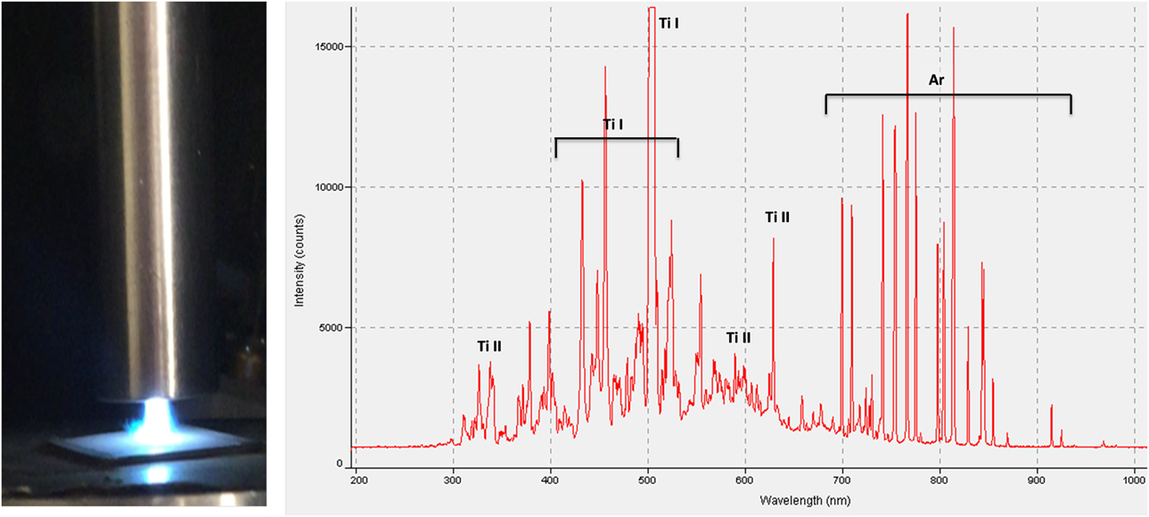
OES provided quantitative plasma diagnostics through measurement of optical emissions from excited states of species, usually formed by electron impact excitation of respective ground-state species. Figure 3 shows the optical emission spectra measured for HiPIPS plasma with a Ti wire interacting with Ar gas. The vertical axes of the figures indicate the number of photons or intensity. All spectra are shown as measured without noise subtraction or numerical processing. A number of atomic lines are clearly observed. The lines observed in the 690–820 nm range are characteristic of Ar in both wavelength and relative intensities [Reference Kramida, Ralchenko and Reader17]. The lines observed in the 320–670 nm range are assigned to Ti I and Ti II [Reference Kramida, Ralchenko and Reader17]. Moreover, the high relative intensity and common transition probability for the Ti I line at wavelength λ = 521 nm and the Ti II line at wavelength λ = 670 nm are present [Reference Kramida, Ralchenko and Reader17]. From the inset photograph, one can clearly see the bright plasma characteristics of HiPIPS.
Photograph (left) and optical emission spectrum (OES) during the operation of HiPIPS with Ar and a Ti wire electrode. OES spectral measurements confirm the presence of Ti* and Ti+* with high photon intensities in the HiPIPS plasma.
The metallic emission line intensities result from a two-step process. First, metallic atoms (Ti, Co, Cr, and Al) are sputtered from the wire by Ar ions:
 $${\rm{A}}{{\rm{r}}^ + } + {\rm{Metal}}\;{\rm{Wire}} \Rightarrow {{\rm{M}}^{ + *}}\quad .$$
Second, these sputtered species are excited either by secondary electrons to form metal excited states:
 $${{\rm{M}}^ + } + {{\rm{e}}^{ - 1}} \Rightarrow {{\rm{M}}^*}\quad .$$
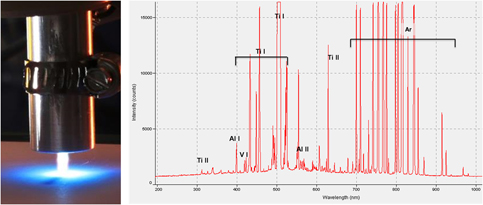
Thus, the OES spectral measurements confirm the presence of Ti* and Ti+* with high photon intensities in HiPIPS plasma. Figure 4 shows an image and the optical emission spectra of an HiPIPS plasma with a Ti–6Al–4V wire interacting with Ar gas. The characteristic Ar lines in the 690 to 820 nm region are observed again. Yet, of more interest are that the spectral lines in the metallic region (320–670 nm), which differ from the spectra of the HiPIPS Ti wire–Ar plasma. The strongest emission lines are still located in the 320 to 670 nm region and are again assigned to Ti I and Ti II transitions. However, new lines are present for Al and V, such as the Al I line at λ = 400 nm and the V I line at λ = 420 nm [Reference Kramida, Ralchenko and Reader17].
Photograph (left) and OES spectrum (right) during the operation of HiPIPS with Ar and a Ti–6Al–4V wire electrode. OES spectral measurements confirm the presence of Ti* and Ti+* along with Al*, Al+*, and V* with high photon intensities in the HiPIPS plasma.

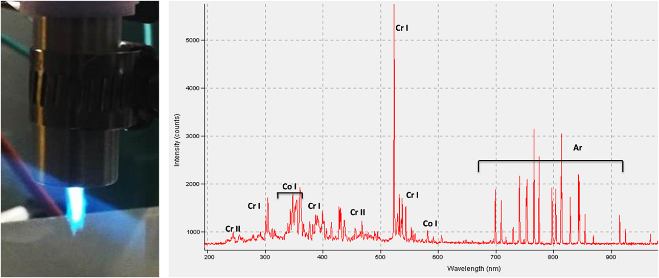
Shown in Fig. 5(a) is an image of HiPIPS in operation with Ar and a CoCr wire electrode. The corresponding optical emission spectra are presented in Fig. 5(b). The spectral lines in the 690–820 nm range are again characteristic of Ar. The strongest emission line at λ = 525 nm is for Cr I. Other numerous Cr I and Cr II lines are present between 220 and 550 nm. Also present are atomic lines for Co I in the 320- to 375 nm region and at λ = 575 and 612 nm [Reference Kramida, Ralchenko and Reader17]. Altogether, the OES spectra have successfully detected and identified charged states of the excited species in the plasma that will ultimately form the deposited coatings.
Photograph (left) and OES spectrum (right) during the operation of HiPIPS with Ar and a CoCr wire electrode. OES spectral measurements confirm the presence of Co*, Cr*, and Cr+*.

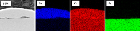
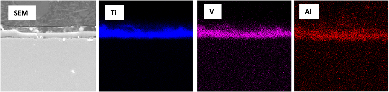
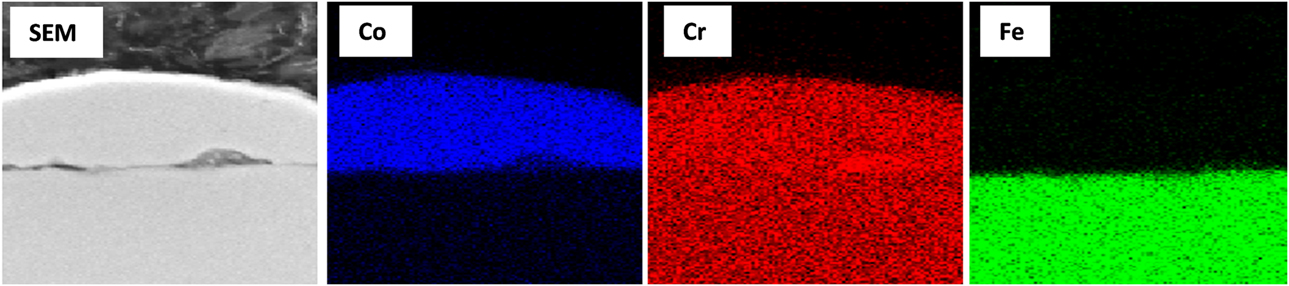
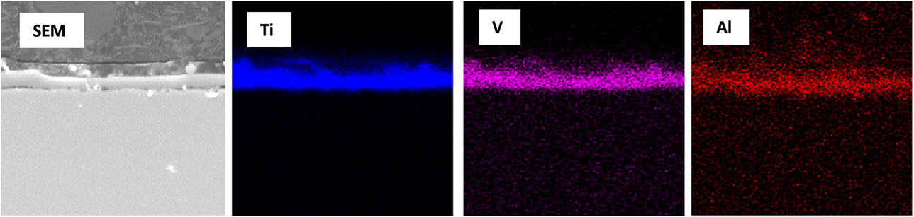
HiPIPS Ti–6Al–4V and CoCr alloy coating deposition process conditions on 4340 steel substrates were developed through a series of trials where a pulsed voltage range of 0.6–2.5 kV with the pulse frequency fixed at 500 Hz and the pulse width fixed at 20 µs, a flow rate of 15 slm of Ar, and a substrate bias range of 70–100 V were utilized. To get to a uniform coating surface coverage, it required at least 8 passes or coating layers. Shown in Fig. 6 are a cross-sectional SEM micrograph and the corresponding EDS elemental maps representative of the HiPIPS CoCr coating. As can be observed in the SEM image, the coating remains adhered after machining and polishing the 4340 steel substrate. The typical coating thickness varied from 1 to 5 µm depending on the deposition time. The average deposition rate was approximately 64 nm/s. EDS mapping analysis reveals that the coating layer contains high amounts and uniform distributions of chromium and cobalt. The elemental composition of the resultant coating can be correlated with the excited species observed in the OES spectra of the HiPIPS CoCr plasma. Likewise, shown in Fig. 7 is a cross-sectional SEM micrograph and the corresponding EDS elemental maps of the HiPIPS Ti–6Al–4V coating. The Ti–6Al–4V coating also remains adhered after machining and polishing the 4340 steel substrate. The EDS elemental maps reveal that the coating layer contains uniform distribution and high amounts of Ti, Al, and V. The elemental composition of the resultant coating can be correlated to the excited species observed in the OES spectra of the HiPIPS Ti–6Al–4V plasma. The nanohardness of HiPIPS thin films were obtained by a nanoindentation technique, where the peak loads ranged from 3000 to 5000 µN. The nanohardness measured for HiPIPS Ti6Al4V and CoCr films ranged from 3.92 to 4.44 and 6.20–8.42 GPa, respectively.
Cross-sectional SEM micrograph (left) and corresponding EDS elemental maps of the HiPIPS CoCr coating on a 4340 steel substrate. EDS mapping analysis reveals that the coating layer contains uniform distribution and high amounts of cobalt and chromium.
Cross-sectional SEM micrograph (left) and corresponding EDS elemental maps of the HiPIPS Ti–6Al–4V coating on a 4340 steel substrate. The coating remains adhered after machining and polishing. EDS mapping analysis reveals that the coating layer contains uniform distribution and high amounts of titanium, vanadium, and aluminum.
Conclusion
In this study, a new version of the atmospheric pressure jet which utilizes advanced high-power pulsed DC generators was developed. Investigations using HiPIPS with Ar and Ti, CoCr, or Ti–6Al–4V wires revealed that high peak power pulses can be achieved (∼70 kW), resulting in high peak currents (∼225 A) and increased ionization and plasma density (n e = 6.23 × 1016 cm−3), while maintaining low average power (40 W) and substrate processing temperatures (<50 °C). The plasma properties of HiPIPS were characterized using current–voltage probes, OES, and a Langmuir probe. OES spectra confirmed the presence of Ti and Ti+, along with Al, Al+, and V, with high photon intensities in HiPIPS plasma with Ar and a Ti–6Al–4V wire. OES spectra confirmed the presence of Co, Cr, and Cr+ with high photon intensities in HiPIPS plasmas with Ar and a CoCr alloy wire. Cross-sectional SEM analysis revealed uniform coatings that ranged in thickness from 1 to 5 μm. EDS mapping analysis revealed that the coating layer contained uniform and high amounts of Cr and Co for HiPIPS CoCr depositions and high amounts of Ti, Al, and V for the HiPIPS Ti–6Al–4V depositions. OES spectra successfully detected and identified charged states of the excited species in the plasma that corroborated the EDS analysis of the elemental composition in the resultant coatings. The HiPIPS technology generates high-density, high-flux plasmas at low temperature and atmospheric pressure conditions for the deposition of metallic coatings. Work is currently underway to further characterize and test the performance of HiPIPS Ti–6Al–4V and CoCr coatings, and examine other HiPIPS coating chemistries.
Experimental
HiPIPS design and operation
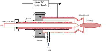
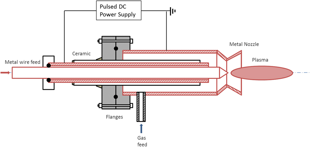
A design for HiPIPS is schematically shown in Fig. 8. The HiPIPS jet head fundamentally consists of a metal wire feed stock (the electrode), a metal tube, a ceramic tube, and a metal nozzle. Metal wires were nominally 0.32 cm in diameter, and metal tubes were nominally 1.2 cm in diameter and 4 cm in length. The metal wire was centered axially in the tube, and the tip was positioned within ≤2 mm from the end of the nozzle. Driven by a pulsed DC power supply (Liaoning Beiyu Vacuum Science and Technology Co., Harbin, China), the HiPIPS jet head was used at atmospheric pressure for various processes, including plasma cleaning and deposition of metallic or ceramic coatings. The HiPIPS plasmas were operated in ambient room conditions without a controlled environment chamber. When the working gas is fed and DC pulses at certain peak voltage, frequency, and pulse width are applied to the center electrode of the HiPIPS, plasma is generated between the electrode and the metal nozzle, resulting in the ablation of the electrode and the nozzle materials. As the DC pulse continues, the current increases dramatically. Because of the high current capability of the advanced power supply design, extremely high peak power can be applied into the plasma within a short period of time. This high power discharge leads to the production of highly ionized gases. The advanced micropulsing capability of the power generator restricts discharge times to values below the time constant for instabilities.
A schematic diagram of the atmospheric pressure HiPIPS system. The line-filled areas represent air gaps.
A number of depositions were carried out to study the effect of deposition parameters, such as pulse power and frequency, precursor gas, and deposition pressure, on the formation of thin films. We employed HiPIPS to generate metallic plasmas at atmospheric pressure using different source metal wires consisting of CrCo alloy, Ti–6Al–4V alloy, and Ti wires (0.125 in diameter). The operating range for HiPIPS during deposition was as follows. High-purity Ar (99.995%) was used as the working gas, and the flow rate controlled by a mass flow controller (MKS Instruments Model 247D, Andover, Massachusetts) was varied from 3 to 20 slm. The pulsed voltage was varied from 0.6 to 2.5 kV, whereas the pulse frequency was fixed at 500 Hz with the pulse width fixed at 20 µs.
The distance between the plasma source and the substrate surface was set to approximately 8 mm. Standard silicon wafers (25 × 25 × 0.75 mm) and 4340 steel coupons (8 × 13 × 0.64 cm) (EMJ Metals, Earle M. Jorgenson Company, Houston, Texas) were used as substrates. Depositions were conducted using a customized X–Y substrate rastering stage. The films were deposited in multiple passes ranging from 3 to 10 passes at a scan velocity of 10 mm/s and a step size of 1 mm. A negative bias ranging from 70 to 120 V was applied to the substrates during deposition. The 4340 steel substrates were mechanically polished to remove existing roughness and surface oxides. All substrates were solvent-cleaned with isopropyl alcohol and air-dried before deposition.
Plasma characterization
OES, electrical probes, and a Langmuir probe were employed for measuring and calculating the plasma characteristics and their variation with systematic changes in HiPIPS process parameters and conditions. An Ocean Optics HR4000CG-UV-NIR spectrometer (Largo, Florida) fitted with a 3648-element linear-array charge-coupled device (CCD) detector provided high-resolution (Δλ = 0.75 nm) emission spectra throughout a 200- to 1000-nm wavelength range. All spectra were acquired through optical fiber at distance of 10 cm between the fiber aperture and the plasma source. Absolute intensity calibrations were performed using two radiance calibration standards traceable to NIST. OES spectroscopic data were acquired without automatic noise subtraction and are shown herein without any numerical processing. The electrical properties of the HiPIPS plasma were studied by measuring the voltage and current transients across the discharge. The measurements were made using a high-voltage probe (Tektronix P6015A, Beaverton, Oregon) and an inductive current monitor (Pearsons Electronics Model 4418, Palo Alto, California). The results were recorded on a digital oscilloscope (Tektronix). A cylindrical-type Langmuir probe (Hiden Analytical Inc. Model ESPion, Warrington, U.K.) was used to measure electron number density (n e) and electron temperature (T e). The probe tip was placed in the plasma region perpendicular to the HiPIPS source at a distance of approximately 9 cm. Bias voltages applied to the Langmuir probe ranged from −10 to 10 V. Note that the Langmuir probe measurements were made in a vacuum chamber at an operating pressure of 0.5 torr (67 Pa). Nonetheless, the electron density is expected to increase with increasing pressure at 760 torr (101 kPa) [Reference Schaub, Hummelt, Guss, Shapiro and Temkin19, Reference Zhou and Dong20, Reference Dawood, Hamdan and Margot21].
Coating characterization
Scanning electron microscopy (JEOL 5800LV SEM, Tokyo, Japan) was used for microstructural examination of the resultant coatings. EDS along with EDS mapping was used to determine film elemental composition. Cross-sectional analysis was conducted on coated 4340 samples that were cut, mounted, and polished. The crystallographic properties of coatings were investigated with an X-ray diffractometer (XRD; Siemens KRISTALLOFLEX 805, Munich, Germany). The nanohardness of HiPIPS thin films were obtained by the nanoindentation technique (Hysitron Triboscope, Eden Prairie, Minnesota). Load-controlled indentation testing followed a trapezoidal loading profile with a hold time of typically 10 s at peak load. Peak loads were ranged from 3000 to 5000 µN. The diamond indenter was a Berkovich tip with a tip radius of 100 nm.
Acknowledgments
This material is based upon work supported by the Strategic Environmental Research and Development Program (SERDP) under Project WP-2608 and by Defense Advanced Research Projects Agency (DARPA) under Contract No. HR001-13-C-008. Views, opinions, and/or findings contained in this report are those of the authors and should not be construed as an official Department of Defense (DoD) position or decision unless so designated by other official documentation.