Introduction
Piezotronics and piezo-phototronics are emerging fields that couple piezoelectricity, semiconducting properties, and photon excitation for achieving high-performance devices,Reference Wu and Wang1–Reference Wang3 such as nanogenerators,Reference Wang and Song4–Reference Qin, Wang and Wang6 piezotronic field-effect transistors,Reference Wang, Zhou, Song, Liu, Xu and Wang7 strain sensors,Reference Zhou, Gu, Fei, Mai, Gao, Yang, Bao and Wang8 light-emitting diodes (LEDs),Reference Yang, Wang, Xu and Wang9 solar cells,Reference Zheng, Zhao, Huang, Nie, Li and Zhang10 strain-gated vertical nanowire arrays,Reference Wu, Wen and Wang11 piezo-phototronic strain sensor arrays,Reference Pan, Dong, Zhu, Niu, Yu, Yang, Liu and Wang12 two-dimensional (2D) piezotronic transistors,Reference Wu, Wang, Li, Zhang, Lin, Niu, Chenet, Zhang, Hao, Heinz, Hone and Wang13 and strain-gated logic devices.Reference Wu, Wei and Wang14 The built-in piezoelectric potential effectively controls carrier-transport characteristics in piezoelectric semiconductors,Reference Zhang, Liu and Wang15–Reference Liu, Zhang, Yang, Niu and Wang18 such as ZnO, GaN, InN, CdS, and monolayer MoS2.
The first piezotronic strain sensor fabricated using a ZnO nanowire showed high strain sensitivity in which the ratio of resistance change to strain (gauge factor) is higher than carbon nanotube devices (∼1000) and reached 1250.Reference Zhou, Gu, Fei, Mai, Gao, Yang, Bao and Wang8 The strain-induced piezoelectric potential modulates carrier-transport properties, generation, and recombination at the junction or interface of a semiconductor. There are two novel features of piezotronic and piezo-phototronic devices. First, piezoelectric materials convert mechanical stimuli to an electric signal; second, strain-induced piezoelectric charges directly control carriers in the depletion layer of a p–n junction or metal–semiconductor contact, which amplifies the piezoelectric signal. Therefore, piezotronic transistors simultaneously have energy/signal conversion and amplification functions, which is the high sensitivity mechanism.
In particular, piezotronic and piezo-phototronic devices exhibit novel sensitivity enhancement for strain-sensing applicationsReference Zhou, Gu, Fei, Mai, Gao, Yang, Bao and Wang8,Reference Zhu, Zhao, Nie, Hu, Li and Zhang19 and energy-conversion improvement for solar cells.Reference Zheng, Zhao, Huang, Nie, Li and Zhang10,Reference Gu, Zheng, Li and Zhang20 Based on semiconductor physics and the piezoelectric theory, the fundamental piezotronic theory has been established, and piezotronic p–n junction and metal–semiconductor contact models have been constructed.Reference Zhang, Liu and Wang15,Reference Liu, Zhang, Yang, Niu and Wang18 Piezotronic and piezo-phototronic effects provide a fundamental understanding of the results of previous theoretical and experimental studies, for example, the piezopotential modulates the Schottky barrier heights at metal–semiconductor contacts,Reference Chung, Wang, Costa, Williamson, Ruden and Nathan21 changes the electric-field distribution in CdS-based photovoltaics,Reference Mitra, Drayton, Cooray, Karpov and Shvydka22 and separates photon-induced electron–hole pairs in core–shell structures.Reference Boxberg, Sondergaard and Xu23
Coupling properties can be used to convert the mechanical or optical signal to ON or OFF output signals. Piezotronic logic devices based on strain-gated transistors have been fabricated for NAND, NOR, and XOR logic units,Reference Wang and Song4 and for piezo-phototronic binary computation using a piezoelectric semiconductor with ZnO and CdS with wurtzite structure.Reference Zhou, Gu, Fei, Mai, Gao, Yang, Bao and Wang8 Piezotronic transistors can be strain sensors, signal comparators and amplifiers, used for designed novel piezotronic analog-to-digital converters for conversion from a continuous-time and -amplitude analog signal to a discrete-time and -amplitude digital signal in strain mapping and digital processing.Reference Nie, Hu, Li and Zhang24 Piezo-phototronics mainly involves the generation and recombination properties of carriers that can be controlled by strain-induced piezoelectric charges.Reference Zhang and Wang16,Reference Liu, Zhang, Yang, Niu and Wang18 Various high-performance piezo-phototronic devices such as solar cells,Reference Zheng, Zhao, Huang, Nie, Li and Zhang10,Reference Gu, Zheng, Li and Zhang20 LEDs,Reference Yang, Wang, Xu and Wang9 and piezo-phototronic photocellsReference Hu, Zhang, Chang, Snyder and Wang25 have been developed. Piezotronic nanodevices with high strain sensitivity, fast response, and low power consumption are good candidates for the Internet of Things (IOT) and self-powered applications. The previously discussed studies not only provide a deeper understanding of piezotronic and piezo-phototronic effects, but also offer guidance for developing high-performance devices.
Here, we summarize current theoretical approaches for piezotronics and piezo-phototronics, including fundamental theory based on semiconductor physics piezoelectric theory, atomistic calculations for simulation-driven material design, and device improvement.
Fundamental theory and device physics
Piezotronic and piezo-phototronic devices had been described using semiconductor physicsReference Sze26 and piezoelectric theory.Reference Ikeda27 The basic equations of interest are the electrostatic, current-density, continuity, and piezoelectric equations, which are utilized for characterizing charge-carrier transport behaviors and photon–electron interactions under a piezoelectric field induced by dynamic straining.
The Poisson equation, one of Maxwell’s equations, describes the charge-induced potential distribution in piezotronic and piezo-phototronic devices:
 $$\nabla ^2 {\rm{\Psi }} = - {{{\rm{\rho }}(r)} \over {{\rm{\varepsilon }}_{\rm{s}} }}$$ ,
where  ${\rm{\psi }}$, ρ(r), and
 ${\varepsilon _s}$ are the potential, the charge density, and the dielectric coefficient, respectively, and r is the position vector.
The current-density equations describe drift and diffusion current density for steady-state conditions:
 $$\left\{ {\matrix{ {{{\bf{J}}_{\rm{n}}} = q{{\rm{\mu }}_{\rm{n}}}n{{\bf{E}}_{{\bf{EL}}}} + q{D_{\rm{n}}}\nabla n} \cr {{{\bf{J}}_{\rm{p}}} = q{{\rm{\mu }}_{\rm{p}}}p{{\bf{E}}_{{\bf{EL}}}} + q{D_{\rm{p}}}\nabla p} \cr {J = {{\bf{J}}_{\rm{n}}} + {{\bf{J}}_{\rm{p}}}} \cr} } \right.$$ ,
where Jn, Jp, and J are the electron, hole, and total current densities, respectively; q is unit electronic charge;  ${\mu _n}$ and
 ${\mu _p}$ are the electron and hole mobility, respectively; n and p are free electron and hole concentrations, respectively; EEL is electric field; and D n and D p are electron and hole diffusion coefficients, respectively.
The time-dependent phenomena are described by the continuity equations for generation and recombination:
 $$\left\{ {\matrix{ {{{\partial n} \over {\partial t}} = {G_{\rm{n}}} - {U_{\rm{n}}} + {1 \over q}\nabla \cdot {{\bf{J}}_{\rm{n}}}} \cr {{{\partial p} \over {\partial t}} = {G_{\rm{p}}} - {U_{\rm{p}}} - {1 \over q}\nabla \cdot {{\bf{J}}_{\rm{p}}}} \cr} } \right.$$ ,
where t is time, G n is electron generation rate, G p is hole generation rate, and U n and U p are the electron and hole recombination rates, respectively.
Applying a small uniform strain S, the polarization P is then given byReference Ikeda27
 $$P = eS ,$$ ,
where tensor (e) is the piezoelectric coefficient.
The constitutive equations can be written asReference Ikeda27–Reference Soutas-Little29
 $$\left\{ \matrix{ {\bf{\sigma }} = {{\bf{c}}_{\bf{E}}}{\bf{S}} - {{\bf{e}}^{\bf{T}}}{\bf{E}} \hfill \cr {\bf{D_{EL}}} = {\bf{eS}} + {\bf{{\rm{\varepsilon }E}} \hfill \cr} \right.$$ ,
where tensors  ${\bf{\sigma }}$ and cE are the stress and elasticity, respectively, DEL is the electric displacement, eT is the transpose of e, and ε is the permittivity tensor.
The piezopotential can change the energy band. A schematic of a piezotronic transistor is shown in Figure 1a. For a one-dimensional p–n junction, the built-in potential  ${\psi _{bi}}$ is obtained as:
 $${{\rm{\Psi }}_{{\rm{bi}}}} = {q \over {2{{\rm{\varepsilon }}_{\rm{s}}}}}\left( {{N_{\rm{A}}}W_{{\rm{Dp}}}^2 + {{\rm{\rho }}_{piezo}}W_{{\rm{piezo}}}^2 + {N_{\rm{D}}}W_{{\rm{Dn}}}^2} \right)$$
where N A and N D are the acceptor and donor concentrations, respectively,  ${\rho _{piezo}}$ is the piezoelectric charge number density, W piezo is width of uniform piezoelectric charge distribution, and W Dp and W Dn are p-side and n-side depletion layer lengths, respectively.
(a) Schematic of a p–n junction-based piezotronic transistor. (Upper) Distribution of the dopants; (middle) potential distribution; and (lower) band structure. Solid line represents the case with piezocharges and the dashed line represents the case without piezocharges. (b) The current–voltage characteristics of an ideal metal–semiconductor contact under different applied strains. The modulation of current by the strain is the result of the piezotronic effect. Reprinted with permission from Reference Reference Zhang, Liu and Wang15. © 2011 Advanced Materials. (c) Gauge factor as a function of strain for a high-sensitivity piezotronic bipolar transistor. The piezotronic effect can remarkably enhance the sensitivity of a bipolar transistor. Reprinted with permission from Reference Reference Zhu, Zhao, Nie, Hu, Li and Zhang19. © 2018 Nano Energy. (d) The capacitance (C i) and (inset) frequency (f) response versus strain in a piezotronic p-insulator-n diode for microwave applications. The frequency characteristics of a piezotronic PIN transistor can be effectively controlled externally. Note: P, polarization; N D, donor concentration; N A, acceptor concentration; W Dp, p-side depletion layer length; W Dn, n-side depletion layer length; W piezo, width of uniform piezoelectric charge distribution; E C, conduction band energy level; E F, Fermi level energy; E V, valence band energy level; J, saturation current density; J C0, saturation current density for a p–n junction; f piezo, frequency in the presence of a piezocharge.

Current–voltage characteristics of the piezotronic p–n junction or metal–semiconductor contact are given by:
 $$J = {J_0}\exp \left( {{{{q^2}{{\rm{\rho }}_{{\rm{piezo}}}}W_{{\rm{piezo}}}^2} \over {2{{\rm{\varepsilon }}_{\rm{s}}}k_{B}T}}} \right)\left[ {{\rm{exp}}\left( {{{qV} \over {k_{B}T}}} \right) - 1} \right]$$ ,
where V is the voltage, k B is the Boltzmann constant, T is temperature, J 0 is the saturation current density, which is J C0 for a p–n junction or J D0 for a metal-semiconductor contact:
 $${J_{{\rm{C}}0}} = {{q{D_{\rm{p}}}{n_{\rm{i}}}} \over {{L_{\rm{p}}}}}exp\left( {{{{E_{\rm{i}}} - {E_{{\rm{F}}0}}} \over {kT}}} \right)$$ ,
where L p is hole diffusion length, n i and E i are the intrinsic carrier density and Fermi level, respectively, and E F0 is the Fermi level without piezoelectric charges and
 $${J_{{\rm{D}}0}} = {{{q^2}{D_{\rm{n}}}{N_{\rm{c}}}} \over {k{T_{}}}}\sqrt {{{2q{N_{\rm{D}}}\left( {{{\rm{\Psi }}_{{\rm{bi}}0}} - V} \right)} \over {{{\rm{\varepsilon }}_{\rm{s}}}}}} exp\left( { - {{q{\phi _{{\rm{Bn}}0}}} \over {kT}}} \right)$$ ,
where N C is the effective density of states at the conduction band,  ${\psi _{bi0}}$ and
 ${\phi _{Bn0}}$ are built-in potential and Schottky barrier height without piezoelectric charges.
The current is an exponential function of strain-induced charges, which can be effectively controlled by tensile or compressive strain. The current–voltage curves of a piezotronic metal–semiconductor contact are shown in Figure 1b. Furthermore, a piezotronic p-insulator-n-structure diode has been demonstrated for high-frequency applications in microwave devices (Figure 1d).Reference Luo, Zhang and Li30 Considering dynamic properties of high-frequency strain, piezotronic and piezo-phototronic devices may broaden conventional applications beyond the static features.Reference Jin, Yan, Wang, Hu, Zhang and Li31 The piezotronic effect on semiclassical ballistic transport prosperities can be studied by the classical Boltzmann equation.Reference Natori32 For monolayer MoS2, the band structure can be calculated by the Schrödinger equation.
Extensive research has been conducted on piezoelectric charges changing the wavelength and enhancing luminescence performance in quantum devices for a wurtzite structure ZnO nanowire, monolayer MoS2, and CdTe quantum dot.Reference Nie, Hu, Li and Zhang24,Reference Zhang and Li33–Reference Li and Zhang35 The coupling between the piezo-phototronics effect and surface plasmonic resonance has been explored both theoretically and experimentally; it has been, for instance, used to enhance the photoluminescence in an InGaN/GaN quantum well.Reference Huang, Jiang, Du, Jing, Liu, Hu and Wang36 In addition, a self-consistent numerical model has been investigated for enhancing the efficiency of solar cells based on InGaN/GaN quantum wells.Reference Jiang, Jing, Huang, Liu, Du, Liu, Pu, Hu and Wang37
Simulation-driven material design and device improvement
Piezotronics and piezo-phototronics have strongly stimulated research on material design and device improvements. The atomistic calculations and semiconductor device simulations play key roles. In one example, two back-to-back bulk ZnO samples with reverse growth directions increased the piezoelectric charge density, based on fundamental theory. The material and device were experimentally realized with an impressive gauge factor of approximately 800.Reference Baraki, Novak, Fromling, Granzow and Rodel38 Another example is the size effect of mechanical and piezoelectric properties of piezoelectric nanowires, which has been studied systematically by the coupling of experimental and computational studies.Reference Espinosa, Bernal and Minary-Jolandan39
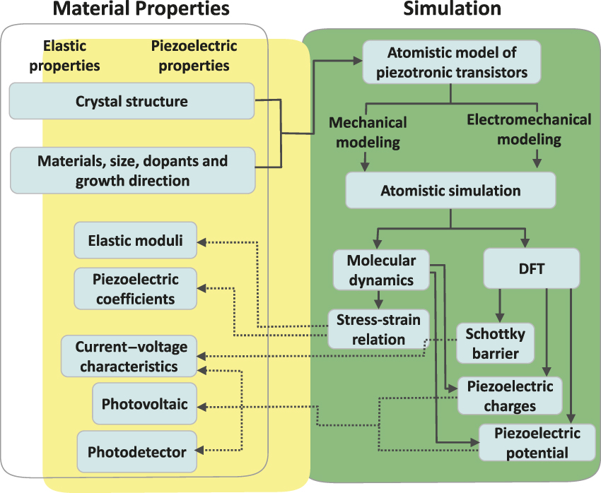
A complete set of semiconductor physics, material simulations, and device design techniques will establish simulation-driven material design and device improvement for piezotronics and piezo-phototronics, as shown in Figure 2. First, materials properties can be obtained from a structural material and with elemental characterization. Second, atomistic calculations, such as the k∙p theory (k is the wave vector and p is the quantum mechanical momentum operator), density functional theory (DFT), and molecular dynamics (MD) yield data on the interface, semiconductor, and piezoelectric properties, are comparable to the results of data from experiments. Third, the calculations and simulations of materials properties can guide and facilitate the design and optimization for piezotronic and piezo-phototronic devices. The development of software packages is also required for the design and simulation of piezotronic and piezophototronic circuits, integrated chips, and sensor networks. Artificial intelligence may provide powerful tools to develop new methods for the search, discovery, and optimization of piezotronic and piezo-phototronic materials.
Materials properties calculations and device simulations of piezotronics and piezo-phototronics. Elastic and piezoelectric properties, including crystal structure, dopant type, and growth direction, are inputted to atomistic simulations based on mechanical and electromechanical modeling. Molecular dynamics and density functional theory (DFT) are then used to calculate the changes induced by the piezoelectric effect to further determine materials properties.

Contact and interface properties
Computational modeling of metal/ZnO contacts in piezotronic devices can be achieved by full atomistic MD simulations.Reference Lei and Leng40–Reference Tan, Xiang, Leng and Leng42 This is a crucial step to understand, from the viewpoint of simulation-driven material and device design, the structure and dynamics at interfaces, and the dependence of device performance on various factors. For example, the Schottky barrier height at metal/ZnO contacts will depend on the size of the contacts and the mechanical stability at the interface during repeated mechanical loadings.Reference Tan, Xiang, Leng and Leng42 Essentially, the total Hamiltonian of a metal/ZnO contact in a piezotronic device should include contributions from both the atomic contact at the interface and mechanical driving systems.Reference Tan, Xiang, Leng and Leng42
For example, in a sliding-bending piezoelectric nanogenerator, the total Hamiltonian at the classical level should be a function of the positions and momenta of all the particles in the ZnO nanowire and metal tip, and the equivalent macroscopic position and momentum of the atomic force microscope cantilever system, together with the elastic potential energy of driving springs, as shown in Figure 3a. MD simulations are also used to study the phenomena of acoustics and acoustic transition radiation that can occur due to the strain-induced polarization, which can sufficiently detect terahertz frequency strain waves at the sub-picosecond level, which approaches atomic time and space resolution.Reference Reed, Armstrong, Kim and Glownia43 Classical core–shell interatomic potentials have been proposed in the study of piezoelectric properties for ZnO nanostructure by MD and molecular statics.Reference Dai, Dunn and Park44 A humidity effect that significantly reduces the piezopotential has also been demonstrated in ZnO nanowires by MD simulations.Reference Zhang and Zhou45 In another study, the piezoelectric constant in collagen was calculated at the pC/N (picocoulomb per newton) level, in agreement with experimental measurements.Reference Zhou, Qian and Minary-Jolandan46
(a) Schematic of (left) molecular dynamics simulation of the mechanical bending of a ZnO nanowire by a metal tip and (right) the associated piezoelectric potential distribution within the ZnO nanowire. The piezopotential is mainly distributed at the contact interface. Reprinted with permission from Reference Reference Tan, Xiang, Leng and Leng42. © 2018 Nano Energy. (b) A Smith chart for a range of 15 lanthanide dopant ions in ZnO for modulating the output emission luminescence properties. The Smith chart shows the energy transmission of doped ZnO with different lanthanide ions. Reprinted with permission from Reference Reference Huang49. © 2017 Physical Chemistry Chemical Physics. (c) First-principles simulation modeling of (i) an Ag-ZnO-Ag piezotronic transistor to (ii) calculate piezoelectric potential; (iii) piezoelectric charge distribution; and Schottky barrier heights for (iv) hcp Ag-ZnO-Ag structure and (v) fcc Ag-ZnO-Ag structure. The piezocharges are mainly distributed at the interface of the metal–semiconductor contact and influence the Schottky barrier height (SBH). Reprinted with permission from Reference Reference Liu, Zhang, Zhang and Wang51. © 2015 Nano Energy. Note:  $\overline {{K_x}}$,
 $\overline {{K_z}}$, elastic coefficients of the spring in the x-axis and z-axis direction, respectively; V, piezopotential; ΔSBH piezo, change in Schottky barrier eight; ΔSBH ZnO(0001)-Ag, Schottky barrier height for the ZnO nanowire along (0001) direction;
 $\Delta SB{H_{{\rm{ZnO}}\left( {000\bar{1}} \right) - {\rm{Ag}}}}$, Schottky barrier height in the (000
 $\bar{1}$) direction; fcc, face-centered cubic; hcp, hexagonal close-packed; M, metal; S, semiconductor.

Semiconductor properties
Considering the current demands of higher sensitivity and lower threshold of mechanical initiation for ZnO-based piezotronic devices, the electronic properties of various ZnO systems have been studied, especially intrinsic defects, to determine the dopable range for further flexible modulations of mechanically induced photoemission.Reference Huang47,Reference Huang, Sun and Peng48 The doping behaviors in material systems (e.g., ZnO) are important for designing piezotronic and piezo-phototronic devices.Reference Huang49 Recent investigations show lower symmetry as the dimensions of the ZnO system decrease. This indicates the electronic range modifiable by doping is substantially enlarged when downscaling the system from three-dimensional to 2D or even lower dimensions, while the decrease in symmetry from crystalline to amorphous makes it difficult to obtain local lattice order. Accordingly, it becomes easier to suppress the local electron–phonon coupling in ZnO via the symmetry relaxation of the local lattice. This is advantageous for adopting a wider doping limit without giving rise to intrinsic deep trapped defects and especially, interference from semicore 4f-electron based rare-earth (RE) ions. This is also the reason why only the low-dimensional ZnO system can achieve bipolar doping. Thus, 2D ZnO is a promising candidate to achieve a wider doping range.
The excited states of lanthanide (Ln) elements in both the divalent (Ln2+) and trivalent (Ln3+) states in a 2D ZnO lattice were extensively studied.Reference Huang49 Trivalent Ln doping follows the removal of the apical dominance concept, in which their electronic transition oscillator strengths are reduced and the excited state energy levels are substantially downshifted to a range below 3.0 eV. This finding contributes more flexible energy transfer for photonic and electronic devices, as shown in the Smith chart in Figure 3b. The Smith chart is used to simultaneously describe photonic–electronic excitation levels and the corresponding oscillator strengths in which the transition oscillator strength has broadened with lattice vibration effects induced by the local piezoelectric field. This can guide the selection or combination of multilanthanide dopants for designing the energy path for an extra-low excitation threshold in piezotronic and piezo-phototronic devices.
Piezoelectric properties
First-principles calculations have been widely used in previous works for calculating piezoelectric coefficients or searching for high-piezoelectric response materials.Reference Momida and Oguchi50 The width of the piezoelectric charge distribution is an important parameter for the band structure and interface engineering. Using DFT, the width of the piezoelectric charge distribution has been calculated in different metal and semiconductor transistors,Reference Liu, Zhang, Zhang and Wang51,Reference Liu, Zhang, Zhang and Wang52 as shown in Figure 3c. Piezoelectric properties of 2D materials have also been determined based on computational predictions and experimental characterization.Reference Hinchet, Khan, Falconi and Kim53 The piezoelectric potential and deformation potential exist simultaneously in the presence of mechanical strain, affecting the luminescence in InGaN/GaN quantum wells.Reference Zhang, Peng, Willatzen, Zhai and Wang54
It was demonstrated by Zhu et al.Reference Zhu, Wang, Xiao, Liu, Xiong, Wong, Ye, Ye, Yin and Zhang55 and Wu et al.Reference Wu, Wang, Li, Zhang, Lin, Niu, Chenet, Zhang, Hao, Heinz, Hone and Wang13 that monolayer MoS2 can exhibit high-piezoelectric coefficients and power output. Piezoelectricity is allowed in MoS2 containing an odd number of layers since these structures lack centrosymmetry, but it disappears in multilayer 2H MoS2 with an even number of layers. It was also concludedReference Wu, Wang, Li, Zhang, Lin, Niu, Chenet, Zhang, Hao, Heinz, Hone and Wang13,Reference Zhu, Wang, Xiao, Liu, Xiong, Wong, Ye, Ye, Yin and Zhang55 that the piezoelectric coefficients of MoS2 degrade rapidly with an increasing number of layers for odd-layered structures. The piezoelectric constant, e 11, was experimentally found to be 2.9 × 10⁻¹⁰ C/m for monolayer MoS2, which is more than a factor of two higher than e 11 for quartz. A high piezoelectric coefficient in 2D monolayer MoS2 is important for electronic and optoelectronic applications of the material.
Fei et al.Reference Fei, Li, Li and Yang56 reported giant piezoelectric constants in monolayer SnSe, SnS, GSe, and GeS based on DFT. For monolayer SnSe, the computed piezoelectric constants were between one and two orders of magnitude larger than for monolayer MoS2 and ZnO structures. The large piezoelectric coecients were attributed to the unique “puckered” C 2ν symmetry of the Group IV elements (the C 2ν group has a twofold symmetry axis and two vertical mirror planes beside the identity operator).Reference Fei, Li, Li and Yang56 Other interesting novel piezoelectric materials for nanogenerator and sensing materials, which can be operated under harsh conditions and with a high Curie temperature T C, include grain-oriented textured PbTiO3 ceramics, for which large piezoelectric voltage coefficients  $g_{33} {\rm{ = - }}\left( {{{\partial E_3 } \over {\partial \sigma _3 }}} \right)_{D} $ were obtained via Sn and Mn doping due to a combination of a high
 $d_{33} = - \left( {{{\partial D_3 } \over {\partial \sigma _3 }}} \right)_{E} $ constant and a relatively small dielectric constant
 ${{\rm{\varepsilon }}_{33}}$.Reference Yan, Zhou, Maurya, Wang and Priya57 Here, σ3 = σzz is the normal stress component in the z direction.
Understanding or prediction of a material’s piezoelectric properties can be facilitated by computation and modeling.Reference Voon and Willatzen58,Reference Barettin, Madsen, Lassen and Willatzen59 Such band structures are provided by the k·p method,Reference Voon and Willatzen60 which in comparison with atomistic models, does not require increased computational power with the number of atoms in the computational domain. Grundmann et al.Reference Grundmann, Stier and Bimberg61 used the 8 × 8 k·p method (eight-band k·p means that two s-type conduction states and six p-type valence states are included in the k·p basis) to demonstrate a significant influence of piezoelectricity on the electronic eigenstates and optical properties of zincblende InAs/GaAs pyramidal quantum dot structures. Andreev and O’ReillyReference Andreev and O’Reilly62 used multiband k·p theory to determine the influence of strain and piezoelectricity on the electronic band structure of GaN/AlN wurtzite quantum dots. Fonoberov and BalandinReference Fonoberov and Balandin63 used continuum elasticity theory and k·p theory to obtain the excitonic properties of strained zincblende and wurtzite GaN/AlGaN quantum dots. Marquardt et al.Reference Marquardt, Boeck, Freysoldt, Hickel, Schulz, Neugebauer and O’Reilly64 presented a versatile code based on continuum elasticity and a 14-band k·p theory for zincblende type structures (14 band refers to the use of six p-type conduction band states, two s-type conduction band states, and six p-type valence band states as the basis for the k·p calculations). Also, Zhang et al.Reference Zhang, Peng, Willatzen, Zhai and Wang54 used a 6 × 6 k·p theory (six-band k·p refers to six p-type valence states are included in the k·p basis), including piezoelectric and deformation potential effects, to describe, in agreement with experiments, strain-dependent luminescence in wurtzite semiconductor quantum-well structures.
Summary
Current theoretical studies have established the fundamental theory and method for research of semiconductor physics, material simulations, and device design techniques of piezotronic and piezo-phototronic devices.
The materials investigated in the previously discussed theoretical and experimental studies are traditional piezoelectric semiconductors. New quantum materials may show promise in obtaining ultrahigh-performance of piezotronic and piezo-phototronic devices. The piezoelectric field in 2D noncentrosymmetric MoS2 is demonstrated to modulate the valley and spin magnetoelectricity. Strain-manipulated valleytronic devices show promise for magnetization switching and detection applications at room temperature.Reference Lee, Wang, Xie, Mak and Shan65 Valleytronic devices make use of quantum manipulation of valleys in the semiconductor energy band structure.
Recently, in quantum acoustics, a piezoelectric semiconductor was shown to have a strong correlation with superconducting qubits due to the large coupling strength of mechanical stimuli and electrical excitations.Reference Chu, Kharel, Renninger, Burkhart, Frunzio, Rakich and Schoelkopf66 The piezoelectric field can also be used to manipulate the quantum states of confined electrons of a gate-controlled quantum dot in GaAs/AlGaAs quantum wells, which leads to a high coefficient of electron-to-mechanics coupling.Reference Okazaki, Mahboob, Onomitsu, Sasaki and Yamaguchi67
Topological insulators in HgTe/CdTe quantum-well structures have been proposed theoretically and verified experimentallyReference Bernevig, Hughes and Zhang68–Reference Chang, Zhang, Feng, Shen, Zhang, Guo, Li, Ou, Wei, Wang, Ji, Feng, Ji, Chen, Jia, Dai, Fang, Zhang, He, Wang, Lu, Ma and Xue70 and hold promise for enabling quantum computers with low energy consumption. Recent theoretical results have suggested that strong piezoelectric field coupling to strain can induce topological insulator states in a GaN/InN/GaN quantum well.Reference Miao, Yan, Van de Walle, Lou, Li and Chang71 The strain-induced piezoelectric field can modulate the quantum point contact in HgTe/CdTe and GaN/InN/GaN quantum wells.Reference Hu, Zhang, Li and Wang72,Reference Dan, Hu, Li and Zhang73 As a consequence of these studies, a piezotronic transistor based on a topological insulator has been proposed,Reference Hu, Zhang, Li and Wang72 as shown in Figure 4. The ON/OFF conductance ratio of this transistor is more than 1010, offering excellent switching behaviors.Reference Hu, Zhang, Li and Wang72 In addition, the piezoelectric potential in a ZnO/poly(3-hexylthiophene-2,5-diyl) nanowire array structure can enhance the room-temperature Rashba spin–orbit interaction, which is momentum-dependent spin splitting in noncentrosymmetric materials.Reference Zhu, Zhang, Lin, Wang, Yang, Chen, Wang, Chen and Wang74 The modulation of spin transport offers strain-gated high-performance spin devices with low energy consumption, thereby providing a platform for discovering new physics.
(a) Schematic of the piezotronic effect in (i) CdTe/HgTe/CdTe topological insulator and (ii) corresponding band structures. The band structure describes the electronic behavior in the quantum point contact (QPC) region. When the piezopotential is absent and the QPC width is larger (i) (top), a topological insulator state results and (ii) (top) gapless band structure is presented. (i) (Bottom) The piezopotential can decrease the QPC width and (ii) (bottom) a gap can be seen in the band structure, which indicates a normal insulator state. (b) Piezotronic effect on the transport properties of a topological insulator based on different piezoelectric materials. (i) Transport conductance plateaus varying with shear strain. (ii) Electronic density distribution in (top) OFF and (bottom) ON states is plotted for narrow and wide QPC widths, respectively. The piezotronic effect can effectively control the electronic transport along the boundaries, and the transistor-based topological insulator has low power consumption. Reprinted with permission from Reference Reference Hu, Zhang, Li and Wang72. © 2017 ACS Nano. Note: k, wave function;  ${\left| \psi \right|^2}$, electronic density distribution; E g, bandgap energy; W_QPC, width of the quantum point contact; I, current;
 $\overline {{G_0}}$, quantum conductance; x, x direction; y, y direction.


Yan Zhang is a professor at the University of Electronic Science and Technology of China. He received his BS degree in 1995 and his PhD degree in theoretical physics in 2004 from Lanzhou University, China. He was an associate professor (2007) and professor (2013) at the Institute of Theoretical Physics at Lanzhou University. He was a visiting scholar and research scientist at Georgia Institute of Technology from 2009 to 2012. His research interests include self-powered nano-/microsystems, piezotronics, and modeling of nonlinear dynamics of nanoelectromechanical systems. Zhang can be reached by email at zhangyan@uestc.edu.cn.

Yongsheng Leng is a professor at George Washington University. He earned his PhD degree in 1999 from Tsinghua University, China. His research interests include contact mechanics and tribology to explore fundamental questions in surface and interfacial science, including liquid structure and dynamics under nanometer confinements, computational nanotribology, membrane fouling mechanisms in water purification, clay swelling in oil and gas recovery, and structure, dynamics, and transport properties of single molecular junctions in molecular electronics devices and metal/semiconductor contacts in energy-harvesting systems. Leng can be reached by email at leng@gwu.edu.

Morten Willatzen is a Talent 1000 Foreign Expert and Senior Full Professor at the Beijing Institute of Nanoenergy and Nanosystems, Chinese Academy of Sciences, China. He also holds a guest professor position in the Department of Photonics Engineering at the Technical University of Denmark, and an Honorary Professorship at the Mads Clausen Institute at the University of Southern Denmark. He received his MSc degree from Aarhus University, Denmark, and his PhD degree from the Niels Bohr Institute at the University of Copenhagen, Denmark. His research interests include solid-state physics, mathematical physics, piezoelectricity, metamaterials, and flow acoustics. Willatzen can be reached by email at morwi@fotonik.dtu.dk.

Bolong Huang has been conducting independent research as a principal investigator at Hong Kong Polytechnic University since 2015. He received his PhD degree in 2012 from the University of Cambridge, UK, and his BSc degree in condensed-matter physics from Peking University, China, in 2007. His research focuses on density functional theory (DFT) calculations on rare-earth functional nanomaterials, defect theory of solid functional nanomaterials, DFT calculations development based on ab initio electronic self-energy corrections, and semi-core orbital corrections as an implement in time-dependent DFT theory. Huang can be reached by email at bolong.huang@polyu.edu.hk.