Introduction
Many semiconductors have been studied over the last century for their possible use in photovoltaics (PVs), light-emitting diodes (LEDs), computing devices, sensors, and detectors. Of these, only a select few have achieved sufficient optoelectronic performance to transition into industrial manufacturing, and their identification and development have been slow and mostly empirical. Recently, high-throughput computation and a deeper understanding of the physics-based requirements for high performance have created the potential for an accelerated identification of functional materials with manufacturing potential. For example, materials screening criteria have been proposed to better focus the search for novel candidate PV materials; they include the optical band-gap energy[Reference Shockley and Queisser1, Reference Prince2] and abruptness of absorption onset,[Reference Yu and Zunger3, Reference Yu, Kokenyesi, Keszler and Zunger4] in addition to boundary conditions of elemental abundance,[Reference Wadia, Alivisatos and Kammen5] and manufacturing cost.[Reference Powell, Winkler, Choi, Simmons, Needleman and Buonassisi6, Reference Surek7] However, many materials have met these criteria and yet have not achieved industrially relevant conversion efficiencies (in excess of 10–15%) due to low minority-carrier lifetimes or diffusion lengths, e.g., in the case of Cu2ZnSn(S,Se)4,[Reference Repins, Moutinho, Choi, Kanevce, Kuciauskas, Dippo, Beall, Carapella, DeHart, Huang and Wei8] SnS,[Reference Mangan, Brandt, Steinmann, Jaramillo, Li, Poindexter, Hartman, Sun, Gordon and Buonassisi9] and others.[Reference Unold and Schock10] Meanwhile, PV devices have emerged based on methyl-ammonium lead iodide (MAPbI3) and closely related halides (herein referred to as MAPbX 3). MAPbI3 is a semiconductor, which has demonstrated exceptional minority-carrier lifetimes of 280 ns (in the mixed iodide–chloride composition)[Reference Stranks, Eperon, Grancini, Menelaou, Alcocer, Leijtens, Herz, Petrozza and Snaith11] and diffusion lengths up to 175 μm,[Reference Dong, Fang, Shao, Mulligan, Qiu, Cao and Huang12] comparable with the best single-crystal semiconductors. This, in addition to meeting the criteria above, has resulted in a dramatic realization of PV conversion efficiencies up to 20.1%[Reference Jeon, Noh, Yang, Kim, Ryu, Seo and Seok13, 14] in 2015, from <4% in 2009.[Reference Kojima, Teshima, Shirai and Miyasaka15]
This paper examines whether the dramatic success of MAPbX 3 in PVs can be used as a basis to expand design criteria to identify new potential high-performance optoelectronic materials. One of the most compelling questions engendered by MAPbX 3 as an optoelectronic material is the degree to which it is unique, and whether its success can lead to the identification of materials with improved stability and lower toxicity, yet similar high performance. Clearly, as in previous design criteria the high optical absorption coefficient is important, but also essential are the long carrier diffusion lengths observed in MAPbX 3, enabled by high minority-carrier lifetime (τ) and mobility (μ).[Reference Stranks, Eperon, Grancini, Menelaou, Alcocer, Leijtens, Herz, Petrozza and Snaith11, Reference Green, Ho-Baillie and Snaith16, Reference Stoumpos, Malliakas and Kanatzidis17] The importance of τ and μ for device performance has been established[Reference Mattheis, Werner and Rau18] for the most highly performing PV materials, including silicon,[Reference Davis, Rohatgi, Hopkins, Blais, Rai-Choudhury, McCormick and Mollenkopf19] cadmium telluride,[Reference Moutinho, Dhere, Al-Jassim, Ballif, Levi, Swartzlander, Young and Kazmerski20, Reference Kranz, Gretener, Perrenoud, Jaeger, Gerstl, Schmitt, Buecheler and Tiwari21] copper indium gallium diselenide,[Reference Repins, Metzger, Perkins, Li and Contreras22] and gallium arsenide.[Reference Miller, Yablonovitch and Kurtz23]
Oddly, these more direct transport parameters, τ and μ, are not traditionally considered essential screening criteria for novel candidate PV materials. This may be partially a consequence of the difficulty in measuring and/or calculating these parameters. The direct measurement of minority carrier τ and μ requires ultrafast electronic or optical sensors to capture transients,[Reference Schiff24–Reference Tiedje, Wronski, Abeles and Cebulka27] or strong steady-state signals,[Reference Sinton, Cuevas and Stuckings28, Reference Katahara and Hillhouse29] and must be performed with PV-device-relevant illumination conditions, electrical fields, and transport directions. Calculating τ and μ from first-principles is even more challenging, given the lack of well-established and high-throughput methods to directly calculate electron–phonon interactions and/or trap capture cross-sections. Although it is possible to obtain some information about carrier mobility from effective masses, and maximum radiative lifetime from the band structure, these are known to be insufficient and can be misleading when point and structural defects limit these transport properties.[Reference Mattheis, Werner and Rau18]
In this paper, we use established recombination models to identify the underlying electronic-structure parameters of MAPbX 3 that are likely to underpin the high experimentally observed τ and μ, including: dielectric constant, effective mass, band bonding character, and band dispersion (i.e., band extrema relative to vacancy levels). We illustrate how these parameters can be computationally accessible using established variants of density functional theory (DFT). Using the basic properties of MAPbX 3 to define a set of search criteria, we discuss the potential to identify other novel materials with “defect-tolerant” transport properties, starting with the database at MaterialsProject.org.[Reference Jain, Ong, Hautier, Chen, Richards, Dacek, Cholia, Gunter, Skinner, Ceder and Persson30] This may yield materials with similar performance, but enhanced stability and lower toxicity.
Redefining search criteria for defect-tolerant semiconductors
This section discusses the emerging explanations for high performance in MAPbI3 and closely related materials, focusing on the unique aspects that make their performance exceptional: specifically their long non-radiative minority-carrier lifetime, even in the presence of defects. A “defect tolerant” material is expected to either (a) form relatively few intrinsic or structural defects under high-throughput, low-temperature processing conditions, and/or more importantly (b) the extrinsic, intrinsic, or structural defects that do form have a very minimal effect on μ and τ. We discuss models of how a material may achieve this defect tolerance, and suggest by example that the underlying electronic-structure properties may not be unique to MAPbX 3, but rather be shared in a broader class of compounds.
Explanations for high performance in methylammonium lead iodide and related materials
Many authors have proposed explanations for the success of MAPbX 3 as a PV material. These include its large absorption coefficient, long electron and hole diffusion lengths, low exciton-binding energies, low effective masses and high mobilities, and the presence of only shallow defects in the band gap.[Reference Stranks, Eperon, Grancini, Menelaou, Alcocer, Leijtens, Herz, Petrozza and Snaith11, Reference Green, Ho-Baillie and Snaith16, Reference Stoumpos, Malliakas and Kanatzidis17, Reference Yin, Shi and Yan31, Reference Yin, Shi and Yan32] The existence of only shallow defects, and the disperse valence band, have both been tied to the presence of filled Pb 6s orbitals, deriving from the partial oxidation of Pb relative to its Pb4+ oxidation state. This orbital character has been identified by several authors, and explains both the shallow binding energy of defects and the atypical dependence of band gap on strain or temperature in MAPbI3.[Reference Yamada, Nakamura, Endo, Wakamiya and Kanemitsu33–Reference Du35] This model for explaining the defect-tolerance and shallow defects has direct analogy to those developed earlier for CuInSe2[Reference Zhang, Wei, Zunger and Katayama-Yoshida36] and Cu3N,[Reference Zakutayev, Caskey, Fioretti, Ginley, Vidal, Stevanović, Tea and Lany37] where instead the Cu+ cation contributes 3d Cu antibonding states to the valence band.
In addition, device-level observations support the claims that MAPbI3 has excellent transport properties, including long carrier diffusion lengths significantly exceeding 1 μm,[Reference Stranks, Eperon, Grancini, Menelaou, Alcocer, Leijtens, Herz, Petrozza and Snaith11] and recently, up to 175 μm in single crystals.[Reference Dong, Fang, Shao, Mulligan, Qiu, Cao and Huang12, Reference Shi, Adinolfi, Comin, Yuan, Alarousu, Buin, Chen, Hoogland, Rothenberger, Katsiev, Losovyj, Zhang, Dowben, Mohammed, Sargent and Bakr38] Low non-radiative minority-carrier recombination rates are also supported by measurements of high photoluminescence quantum yield,[Reference Tvingstedt, Malinkiewicz, Baumann, Deibel, Snaith, Dyakonov and Bolink39] long carrier lifetimes,[Reference Miller, Zhao, Mercado, Saha, Luther, Zhu, Stevanovic, Perkins and van de Lagemaat40] and the high open-circuit voltage (V OC) demonstrated by many devices. These properties are made more exceptional by the way in which MAPbI3 is processed: low-temperature solution processing results in equal or better performance to vacuum synthesis, which runs contrary to the higher purity, higher temperature, and more equipment-intensive fabrication strategies used to obtain high performance in conventional crystalline semiconductor materials.
We substantiate these earlier reports by applying DFT to MAPbI3. In the model pioneered by Zhang,[Reference Zhang, Wei, Zunger and Katayama-Yoshida36] as well as Lany and Zakutayev,[Reference Zakutayev, Caskey, Fioretti, Ginley, Vidal, Stevanović, Tea and Lany37] defect tolerance emerges from having bonding orbitals at the conduction band minimum (CBM), and antibonding orbitals at the valence band maximum (VBM). This band structure is markedly different than that in most semiconductors, where the valence band is composed predominantly of bonding states, whereas the conduction band is composed of wavefunctions with dominant antibonding character. The defect tolerance that emerges from such an electronic structure is easily described using atomic vacancies as examples. Namely, if predominantly antibonding orbitals occur at the VBM and bonding at the CBM, the dangling (broken) bonds that are formed upon creating the vacancy (of any kind) will likely appear as resonances inside the bands, leaving the band gap free of deep states that could act as carrier traps. As shown in Fig. 1 for the valence band of MAPbI3, this is a consequence of the position of valence atomic orbitals relative to the bonding and antibonding bands formed due to interactions. Analogous arguments are also valid for other types of intrinsic defects, such as interstitials and/or antisites, as well as for structural defects such as grain boundaries, which consist of many strained and dangling bonds. Extrinsic impurities could, however, still introduce deep traps inside the band gap depending on the position of their atomic orbitals relative to the energy bands of the host material.
(a) Crystal structure of cubic (high T) phase MAPbI3, including the MA cation at the cage center; (b) bonding (σ)/ antibonding (σ*) orbitals in MAPbI3 demonstrating the formation of energy bands relative to isolated p and s atomic orbital energies; (c) DOS of MAPbI3 separated into cation and anion s- and p-orbital contributions. The DOS is computed using DFT, including the effects of SO interactions, with the band gap adjusted to the value reported in Ref. Reference Miller, Zhao, Mercado, Saha, Luther, Zhu, Stevanović, Perkins and van de Lagemaat42 (1.85 eV computed using the many body GW method with SO included). The MA+ cation does not introduce states at the band edge.

These situations, in particular the antibonding character of the VBM, can frequently be found in metal–non-metal systems with partially oxidized cations such as binary group-III halides or group-IV chalcogenides in 1:1 stoichiometry (e.g., TlBr and SnTe). Owing to the partial oxidation of Pb, the MAPbI3 compound also exhibits similar electronic-structure features.[Reference Umebayashi, Asai, Kondo and Nakao41] As shown in Fig. 1, there are three types of interactions that contribute to the valence band in MAPbI3. The first results from the overlap of Pb(6p)–I(5p) atomic orbitals leading to the creation of the deeper portion of the valence band, which is predominantly of I(5p) character, and the bottom part of the conduction band, which is composed mostly of Pb(6p) atomic orbitals. This interaction is responsible for chemical bonding as it implies charge transfer from the Pb(6p) to the I(5p) orbitals. In addition, Pb(6s)–I(5p) interaction leads to the creation of two bands: a deeper valence band (bonding), and the antibonding maximum of the valence band. Finally, only one of the I(5p) orbitals is oriented along the Pb–I bond, which is a favorable direction to interact with Pb(6s) and Pb(6p). The other two, oriented orthogonally, can only interact with the 5p orbitals from other iodine atoms forming the middle of the valence band as shown in Fig. 1.
As a result of these interactions, the electronic band gap is formed between the antibonding top of the valence band originating from the Pb(6s)–I(5p) interactions and the antibonding CBM resulting from the Pb(6p)–I(5p) interactions. Bonding-type defect-tolerance arguments can therefore only be applied to the defects that would tend to create valence band-derived states such as cation (Pb or MA) vacancies. On the other hand, if anion (iodine) vacancies form, the resulting dangling bonds will appear as resonances inside the conduction band only if the bandwidth and the dispersion of the conduction band are such that the CBM falls well below the energy of the Pb(6p) atomic orbitals. In the case of Pb, contrary to Sn and Ge compounds for example, this condition is more likely due to relativistic[Reference Umari, Mosconi and De Angelis43] SO interaction effects that increase the width of the Pb(6p) conduction band by ~2 eV based on our calculations. Thus, the fact that vacancy-type defects in MAPbI3 are resonant in the bands is attributed to: (a) the presence of antibonding orbitals within the valence band that push the VBM energy up, and (b) relativistic effects which push the CBM energy down.
In summary, an emerging conclusion from both experimental measurements and first-principles calculations is that MAPbX 3 benefits from an inherently defect-tolerant electronic structure.
Modeling electronic transport in the presence of defects
To provide physical context for the claims above, and to translate them into electronic-structure design criteria, we focus on transport models in defective materials: in particular, models for defect-assisted μ and τ. These are semiconductor models (distinct from the Langevin recombination model, which is inappropriate for MAPbI3).[Reference Miller, Zhao, Mercado, Saha, Luther, Zhu, Stevanovic, Perkins and van de Lagemaat40]
Defect-limited, monomolecular, or trap-assisted non-radiative recombination, U SRH, is modeled by Shockley–Read–Hall (SRH) recombination statistics:
 $$U_{\rm SRH} = \displaystyle{{np - n_{\rm i}^2} \over {{\tau _{0,{\rm h}}}(n + {n_1}) + {\tau _{0,{\rm e}}}(\,p + {\,p_1})}}\;, $$
where n, p, and n i are the electron, hole, and intrinsic carrier concentrations, respectively.[Reference Sze and Kwok44] The low-injection electron and hole lifetimes τ 0,e and τ 0,h, which we seek to maximize, are:
 $${\tau _{0,{\rm h}}} = \displaystyle{1 \over {{N_{\rm t}}{\sigma _{{\rm t},{\rm h}}}{v_{{\rm th},{\rm h}}}}} \quad {\rm and}\quad {\tau _{0,{\rm e}}} = \displaystyle{1 \over {{N_{\rm t}}{\sigma _{{\rm t},{\rm e}}}{v_{{\rm th},{\rm e}}}}}, $$
where N t is the trap density, σ t is the capture cross-section for electrons or holes, and v th is the drift velocity of carriers. At low injection conditions, the hole and electron lifetimes tend toward τ h = τ 0,h and τ e = τ 0,e, respectively; at high-injection conditions, both hole and electron lifetimes tend toward τ h = τ e = τ 0,h + τ 0,e. The terms n 1 and p 1 reflect the occupancy of trap states, where E t is the energy level of the trap state and E i the Fermi level in the intrinsic material (near mid-gap):
 $${n_1} = {n_{\rm i}}{\rm exp}\left( {\displaystyle{{{E_{\rm t}} - {E_{\rm i}}} \over {kT}}} \right)\quad {\rm and}\quad {\,p_1} = {n_{\rm i}}{\rm exp}\left( {\displaystyle{{{E_{\rm t}} - {E_{\rm i}}} \over {kT}}} \right). $$
From this model, three conditions are necessary to limit SRH (trap-assisted) recombination: defect energy levels far from mid-gap, as these exponentially impact lifetime; low trap density N t; and low capture cross-sections σ. Operating in high-injection conditions is helpful (where photogenerated carrier concentrations greatly exceed background doping densities), especially when strongly injection-dependent defects limit lifetime. E t and N t may be calculated from first-principles; however, this calculation is computationally expensive, so we seek more fundamental electronic properties accessible by high-throughput screening.
The first, and most important property is the relative static permittivity, or dielectric constant ε r. A higher dielectric constant indicates a greater ability to screen charge, and may arise from electronic or ionic contributions, as well as the methylammonium molecular dipoles in the lattice.[Reference Frost, Butler, Brivio, Hendon, van Schilfgaarde and Walsh45]
This screening means that the capture cross-section of a charged defect will be influenced by the dielectric constant. Assuming a Coulombic model for capture cross-section, a capture event will occur when the electrostatic potential energy from a charged defect exceeds the thermal energy, kT, which occurs at a specific radius,[Reference Bube46] therefore:
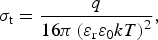 $${\sigma _{\rm t}} = \displaystyle{q \over {16\pi\, {{({\varepsilon _{\rm r}}{\varepsilon _0}kT)}^2}}}, $$
where q is the elementary charge, and ε 0 is the vacuum permittivity. MAPbI3 has demonstrated a large static dielectric constant of 60–70 or higher,[Reference Green, Ho-Baillie and Snaith16, Reference Lin, Armin, Nagiri, Burn and Meredith47, Reference Juarez-Perez, Sanchez, Badia, Garcia-Belmonte, Kang, Mora-Sero and Bisquert48] due to electronic, ionic, and molecular dipole contributions from the organic cation.[Reference Brivio, Walker and Walsh49] This charge screening is very beneficial, given the inverse square dependence of carrier capture cross-section, and in turn recombination rate, on the dielectric constant.
In addition, for a simple “hydrogenic” defect under Effective Mass Theory, the energy level of the defect sits deeper in the gap for lower dielectric constants,[Reference Sze and Kwok44] i.e. the binding energy of a donor relative to the conduction band, E C is:
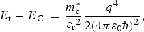 $${E_{\rm t}} - {E_{\rm C}}\; = \displaystyle{{m_{\rm e}^{\ast}} \over {{\varepsilon _{\rm r}}^2}} \displaystyle{{{q^4}} \over {2{{(4\pi {\varepsilon _0}\hbar )}^2}}}, $$
where m*e is the effective mass of an electron, and ħ is the reduced Planck constant. Similar charge screening behavior has been used to explain the low binding energy of excitons in MAPbI3[Reference Frost, Butler, Brivio, Hendon, van Schilfgaarde and Walsh45] and shallow effective mass-like states.[Reference Kim, Lee, Lee and Hong50]
More important, however, is the energy level of non-effective-mass like traps formed by vacancies and structural defects. As discussed above, band structures containing antibonding orbitals in the VBM, bonding in the CBM, and/or high dispersion within a band can lead to shallower defects, as defect energy levels are resonant with the conduction or valence bands. A second model proposed to explain the lack of deep trap states is that MAPbI3 is more ionic than other semiconductors,[Reference Kim, Lee, Lee and Hong50] resulting in shallower or fewer defect states associated with dangling bonds. Analogous arguments have been made to explain defect tolerance in GaN[Reference Lester, Ponce, Craford and Steigerwald51] and (Cd, Zn)Te.[Reference Carmody, Mallick, Margetis, Kodama, Biegala, Xu, Bechmann, Garland and Sivananthan52]
The second critical transport property is the minority-carrier mobility, which is influenced by the effective masses of free carriers and by the frequency of scattering events. The lower the effective mass, or the more disperse the band edges, the higher the mobility. However, in typical polycrystalline materials at room temperature, the mobility will not reach this intrinsic limit due to several forms of scattering.
One way in which the mobility will be limited is by charged defect scattering, either at ionized impurities or grain boundaries. Again, a high dielectric constant reduces the spatial extent and the potential barrier of a charged defect, lowering its propensity to scatter free carriers. For ionized impurities, the mobility μ H,ii is given by:
 $${\mu _{{\rm H},{\rm ii}}} = {r_{{\rm H},{\rm ii}}}\displaystyle{{128\sqrt {2\pi}\, {{\left( {{\varepsilon _{\rm r}}{\varepsilon _0}} \right)}^2}{{(kT)}^{3/2}}} \over {\sqrt {{m ^{\ast}}{N_{\rm t}}{Z^2}{e^3}}}} {\left[ {\ln (1 + b) - \displaystyle{b \over {1 + b}}} \right]^{ - 1}}, $$
where r H,ii is the Hall coefficient for ionized impurity scattering, Z is the charge on the ionized site, N t is the trap density, b = 24m*kT/ħ 2β S2, and β S is the inverse screening length.[Reference Lee, Winkler, Siah, Brandt and Buonassisi53] Thus, to reduce the impact of ionized impurities on mobility, it is again ideal to have a high dielectric constant, low effective mass, and low trap density. Grain boundary scattering is also reduced for larger dielectric constants, and when the defect levels associated with grain boundaries become shallower.[Reference Seto54]
Alternatively, the mobility limit may come from phonon scattering. The phonon-limited mobility is generally smaller in softer materials, given their higher concentration of phonons at a given temperature—the bulk modulus, B, and phonon-limited mobility μ ph are correlated,[Reference Yan, Gorai, Ortiz, Miller, Barnett, Mason, Stevanović and Toberer55] where A 0 is a constant:
 $${\mu _{{\rm ph}}} = {A_0}B{({m ^{\ast}})^{ - 2.5}}. $$
MAPbI3 is a relatively soft material, with a bulk modulus predicted to be 22.2 GPa for the cubic phase.[Reference Feng56] This may explain why its mobility, measured about 10 cm2/V/s,[Reference Miller, Zhao, Mercado, Saha, Luther, Zhu, Stevanovic, Perkins and van de Lagemaat40] is not large relative to III–V and group IV semiconductors. Claims of “high” mobilities may be relative to dyes and organic absorber materials from which much of the perovskite PV work derived. Thus, similar to the absorption coefficient of MAPbI3, its mobility is necessary but insufficient to explain its high performance.
To compare these proposed performance criteria for PV, the ratio of the diffusion length to the absorption length in an absorber material must be maximized to produce high photocurrent in a PV device, as in this non-dimensional figure of merit[Reference Krich, Halperin and Aspuru-Guzik57]:
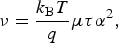 $$\nu = \displaystyle{{{k_{\rm B}}T} \over q}\mu \tau {\alpha ^2}, $$
while historical PV screening approaches have focused on maximizing α; here instead we focus on τ. Given that the mobility and absorption coefficient are good, but not exceptional for MAPbI3, we suggest that it is the minority-carrier lifetime of MAPbI3 that is most strongly responsible for its exceptional performance.
Finally, it is worth mentioning that beyond point and structural defects, a disordered crystal structure can limit the conversion efficiency by introducing defect states near the band edges (Urbach tail). MAPbI3 demonstrates a very small Urbach tail energy.[Reference De Wolf, Holovsky, Moon, Löper, Niesen, Ledinsky, Haug, Yum and Ballif58] This may be due to its low melting temperature, such that the material develops more crystalline order at lower processing temperatures (high homologous temperatures).[Reference Green, Ho-Baillie and Snaith16]
To review, we summarize the priorities for high-performance PV absorbers in Fig. 2. While prior work has focused on screening for optical properties, we focus specifically on electronic-structure properties that have a direct impact on transport, highlighted in bold.
Screening criteria for high-performance PV materials, focusing on the properties that enable excellent bulk transport in the presence of defects. Optical properties and scalability concerns have previously been emphasized in screening, and are important but insufficient to achieve high performance.
Toward ideal electronic structure: the importance of partially oxidized, heavy post-transition metals
Materials that contain a lone 6s 2 or 5s 2 pair of electrons on the cation have the potential to share the high dielectric constant, low effective masses, and VB antibonding character that lead to defect tolerant transport properties. As a broad class, these are compounds formed from partially oxidized post-transition metals including In, Sn, Sb, Tl, Pb, and Bi. In the case of MAPbI3, the partially oxidized Pb atom in its Pb2+ charge state lends these beneficial properties—a large, polarizable cation leads to high Born effective charge and therefore large dielectric constants,[Reference Du35] as well as a conduction band with greater bandwidth due to SO coupling, while filled 6s orbitals lead to a disperse valence band (low effective mass)[Reference Yin, Shi and Yan32] and antibonding orbital character in the VBM.
Other partially oxidized post-transition metals including In+, Sn2+, Sb3+, Tl+, Pb2+, and Bi3+ share these properties, and are present in a wide variety of materials. This N-2 oxidation state is more commonly observed for compounds of Tl, Pb, and Bi, due to relativistic effects leading to tighter binding of the remaining s electrons; however, lighter cations may also be stabilized in these oxidation states. Given their many beneficial properties, these cations appear increasingly in many optoelectronic applications: PbS and lead halide perovskites in PV; TlBr, PbI2, and BiI3 in x-ray detectors and scintillators[Reference Sellin59]; Sn2+-based TCOs[Reference Hautier, Miglio, Ceder, Rignanese and Gonze60]; and Pb- and Bi-based ferroelectrics, photoferroelectrics,[Reference Nechache, Harnagea, Licoccia, Traversa, Ruediger, Pignolet and Rosei61] piezoelectrics,[Reference Rödel, Jo, Seifert, Anton, Granzow and Damjanovic62] and thermoelectrics. For the thallous halides, analogous 6s 26p 0 orbital explanations for low effective mass, antibonding VBM states, and a high dielectric constant were offered several years before similar work on MAPbX 3.[Reference Mudring63, Reference Du and Singh64, Reference Du and Singh65]
To identify promising materials in this class, we developed a script to search through all materials in the Materials Project.org (MP) database.[Reference Jain, Ong, Hautier, Chen, Richards, Dacek, Cholia, Gunter, Skinner, Ceder and Persson30] This is implemented using the Materials Project API and the pymatgen library, to access information on calculated crystal and electronic structure for all compounds in the database.[Reference Ong, Richards, Jain, Hautier, Kocher, Cholia, Gunter, Chevrier, Persson and Ceder66] This search examines approximately 27,000 non-metallic inorganic compounds with full band structures calculated, and extracts information on crystallographic point group, stability, band structure, and in particular the fractional DOS by element and orbital. To screen for the properties described above, we calculate the s-orbital fraction in the top 1 eV of the valence band DOS. This metric is a rough filter, and may mistakenly identify materials with band-inversion, as well as many metal hydrides and Au− compounds, wherein the anion species contributes a filled s orbital at the valence band edge.
In Fig. 3, we compare a random subset of the materials identified in this broad search, and note the stark differences in VBM DOS character for different classes of materials. Conventional tetrahedrally coordinated III–V and II–VI compounds all demonstrate almost exclusive p-orbital character at the VBM, as do the majority of compounds. Other defect tolerant Cu-chalcogenide semiconductors, such as CuInSe2, demonstrate a large d-orbital character in the valence band due to full 3d cation orbitals. Meanwhile, the inorganic I–II–VII3 family of perovskites sit along the bottom axis, reflecting their larger s-orbital fraction in the valence band DOS. However, they are not unique in this property. In addition, we plot a random fraction (30%) of the Materials Project Sn-cation compounds on these axes as well, separating them by those with Sn2+ and Sn4+ cations. The Sn2+ cation-compounds cluster in the same region as the halide perovskites, whereas Sn4+ compounds resemble the vast majority of semiconductors with anion p-orbital or transition metal cation d-orbital character.
Ternary plots demonstrating the partial DOS of the VBM by orbital type, for a wide range of randomly selected materials. Overlayed on the left are the conventional zincblende and wurtzite semiconductors for PV, as well as Cu-chalcogenides showing higher d-orbital fraction, and the halide perovskites with higher s-orbital fraction. On the right, Sn-containing compounds demonstrate a distinct split along two axes, with Sn2+ compounds demonstrating similar character to the halide perovskites.
Finding good candidate semiconductors with the N-2 oxidation state is not straightforward, for several reasons. Firstly, the use of more electronegative anions (oxygen, fluorine, and chlorine) tends to fully oxidize these cations. By pairing them with sulfur, selenium, iodine, and bromine, or by including a less electronegative cation such as an alkali metal, it is possible to stabilize the lower oxidation state. Secondly, the lone s orbitals are often stereochemically active,[Reference Walsh, Payne, Egdell and Watson67] leading to lower symmetry point groups, and a higher likelihood of indirect gaps. For example, for Sn compounds from the Materials Project database, only 29% of those with Sn2+ are found to have direct band gaps, whereas for Sn4+, 47% have direct band gaps. Anisotropic crystal structures may also lead to anisotropic transport properties and surface potentials,[Reference Stevanović, Hartman, Jaramillo, Ramanathan, Buonassisi and Graf68] which may adversely influence device performance. Lastly, these cations may convert to the higher oxidation states inadvertantly, when exposed to oxidizers such as oxygen or moisture. In CsSnI3 and MASnI3, this Sn4+ formation results in metallic behavior with very high carrier concentrations.[Reference Walsh34, Reference Chung, Song, Im, Androulakis, Malliakas, Li, Freeman, Kenney and Kanatzidis69]
Lastly, we note that all of the materials identified in the MaterialsProject.org search are inorganic, and we recognize the important role that the asymmetric, molecular cations such as methylammonium play in achieving large dielectric constants in these materials. Converting the inorganic materials identified herein into hybrid organic–inorganic analogues could lead to improved defect tolerance, but the presence of MA or other molecular cations is not the most important criteria in achieving defect tolerance. Thus, replacement of Pb in MAPbX 3 with transition metal cations may not yield high-performing semiconductors.
Outlook: identifying other promising materials classes with excellent transport properties
By filtering the materials data drawn from the Materials Project database, we focus on several interesting classes that may share the beneficial properties identified above. Our search first identifies the class of halide perovskites (CsPbI3, CsSnI3, RbPbBr3, etc.); to our knowledge prior optoelectronic screening efforts have not identified these as promising materials.
In the list below, we exclude Pb2+ and Tl+-containing compounds based on toxicity; there are many promising optoelectronic materials containing these atoms. Unfortunately, the beneficial properties of Pb2+ and Tl+ are also connected to their toxicity, as they mimic the large ionic sizes of Ca2+ and K+ in the human body. This excludes the binary lead and thallium halides and chalcogenides such as TlBr, as well as a number of ternary chalcohalides or chalcogenides such as TlBiS2.
In addition, this search is limited to materials existing in the MaterialsProject.org database. New materials may be discovered or designed using the present framework, for example the recently discovered Bi2FeCrO6 perovskite,[Reference Nechache, Harnagea, Li, Cardenas, Huang, Chakrabartty and Rosei70] which achieves an unusually small band gap for a complex oxide ferroelectric, and promising PV performance.
We compute the electronic structure from first-principles for several classes of materials, which were identified through the broad computational survey. These classes are described below:
(i) Binary chalcogenides and halides (BiI3, Bi2S3, SbI3, Sb2S3, SnI2, InI, etc.): There are many binary iodides, sulfides, and selenides formed with ns 2np 0 cations, several of which have band gaps in the range of interest for PV. Those with band gaps 1.7 eV and greater, such as BiI3, PbI2, and TlBr, have been demonstrated successfully in x-ray detecting and scintillator applications, with high μτ products.[Reference Sellin59, Reference Mudring63, Reference Lintereur, Qiu, Nino and Baciak71]
(ii) Binary halides, sulfides, and selenides stabilized in cubic structures such as NaCl and CsCl: Given the anisotropic transport properties that result from stereochemically active lone pairs in materials such as SnS, more promising materials may result by stabilizing them in higher symmetry phases. Recently, it was demonstrated that SnS and SnSe may be stabilized in the NaCl structure by alloying with CaS.[Reference Vidal, Lany, Francis, Kokenyesi and Tate72] Similarly, TlI may be stabilized in the CsCl phase by alloying,[Reference Secco and Sharma73] suggesting a possible similar route with InI.
(iii) Chalcohalides (BiOI, BiSI, BiSeI, SbSI, SbSeI, BiSBr, BiSeBr, etc.): The ns 2np 0 chalcohalides (V–VI–VII compounds) range over visible to UV band gaps,[Reference Nitsche and Merz74] and many demonstrate ferroelectric behavior at lower temperatures as well. Both Sb- and Bi-containing varieties have demonstrated photoconductive or PV effects.[Reference Hahn, Rettie, Beal, Fullon and Mullins75–Reference Zhao, Zhang and Zhang78] SbSI and SbSeI have recently been identified for their potential applications as photoferroelectrics[Reference Butler, Frost and Walsh79]; however, those in the paraelectric phase may still demonstrate large Born effective charge, and a large static dielectric constant.
(iv) Ternary alkali chalcogenides (LiBiS2, NaBiS2, KBiS2, RbBiS2, CsBiS2, etc.): Similar to the formation of I–III–VI2 analogues of the zincblende II–VI compounds, one may form I–III–VI2 rocksalt compounds based on the PbS and PbSe rocksalt phases.[Reference Gabrel'yan, Lavrentiev, Nikiforov and Sobolev80–Reference McCarthy, Ngeyi, Liao, DeGroot, Hogan, Kannewurf and Kanatzidis82] These include Pb-free chalcogenides with an octahedrally coordinated Bi3+ cation.
(v) Ternary halides: (In3SnI5, InAlI4, etc.): In+ and Tl+ may be stabilized by several non-coordinating molecular anions such as AlI4–.[Reference Timofte and Mudring83] In addition, multiple cations can be stabilized in their lower oxidation states together, as in Sn2+ and In+ in the case of In3SnI5.
(vi) In+–II–VII 3ternary halides (CdInBr3, CaInBr3, etc.): In+ is also stabilized in a number of In–II–VII3 compounds, which appear to have band gaps outside of the range for PV, but which may exhibit similar defect tolerant properties.
(vii) Bismides and antimonides (e.g., KSnSb): Sn2+ and other partially oxidized cations are stabilized in several bismides and antimonides, most of which have band gaps too small for PV absorbers under 1-Sun illumination.
(viii) Octahedrally coordinated metal halides (Cs3Bi2I9, Rb3Bi2I9, K3Bi2I9, Cs3Sb2I9, etc.): Bi3+ and Sb3+ form III2X93– anions that consist of edge or face-sharing octahedra, bonding with alkali metals to form a variety of materials with different band gaps, crystal structures, and ferroelectric phase transitions.[Reference Mel'nikova and Zaitsev84–Reference Wu, Wu and Chen87]
(ix) Cs-containing compounds substituting 1+ molecular cations [e.g., (MA)3Bi2I9, (FA)3Bi2I9, etc.]: Lastly, we can identify a variety of Cs-containing materials, which could be converted to hybrid materials by the substitution of the Cs with an alkylammonium or other molecular cation.[Reference Jakubas and Sobczyk86, Reference Plackowski, Wlosewicz, Tomaszewski, Baran and Marchewka88] A simple example is the family containing (MA)3Bi2I9 or (FA)3Bi2I9 (with formamidinium as the organic cation). A number of other molecular cations may be substituted as well based on size, analogous to the substitution explored in MAPbX 3,[Reference Kieslich, Sun and Cheetham89, Reference Filip, Eperon, Snaith and Giustino90] to tune the band gap or to form lower-dimensional structures.
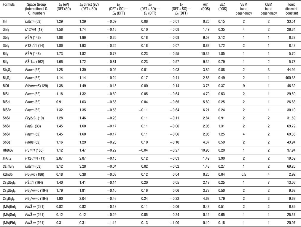
As an illustration, we perform first-principles (DFT) calculations on some of the above-listed materials to probe whether these materials have low effective masses and high static dielectric constants, in addition to containing cation antibonding orbitals in the VB, and compare these results with those of MAPbI3. These DFT results are summarized in Table I, including the band gap (E G), relative valence band (E V) and conduction band energies (E C), effective masses m* for holes and electrons from the DOS, the band degeneracy at the CBM and VBM extrema, and the ionic dielectric constant. DFT calculations are performed with SO coupling; we compare the band extrema energies with and without SO coupling to demonstrate the relativistic effects. DFT is known to consistently under-predict the band gap, thus, we do not present the electronic component of the dielectric constant. Instead, we present only the ionic dielectric constant computed from density functional perturbation theory. In addition, the band-gap values, both the minimum and the direct gap, are given to provide an indication of the type of optical transition at the lowest energy gap. The larger the difference between the minimal and the direct gap, the weaker the absorption onset is. More information on these calculations is supplied in the Methods section.
It is important to draw attention to several conclusions from this table. Firstly, many of these materials are relatively ionic, like MAPbI3, making it difficult to achieve smaller band gaps (note again that the band gaps presented here are underestimated, and many will be >2 eV in reality). Secondly, anisotropic crystal structures with stereochemically active lone pairs often lead to higher hole effective masses. Thirdly, most of the materials presented here demonstrate large ionic dielectric constants, independent of whether they have a polar space group. It is clear that MAPbI3 offers an unusual mix of ionicity, high dielectric constant, low effective masses, and a lower band gap for PV; few semiconductors can claim excellent performance across all categories.
Another conclusion consistent with prior observations is that compounds formed with 6p block cations show a significantly larger contribution of SO coupling in the conduction band, versus those formed from the 5p block. While Pb and Tl compounds are not included here, the Bi compounds show a much stronger SO contribution than do the In, Sn, and Sb compounds. This may suggest that the Bi-containing compounds are most suitable for achieving similarly shallow anion vacancy levels as in MAPbI3.
To illustrate the similarities in band structure to MAPbI3, the band orbital diagrams and DOS are presented in Fig. 4 for a handful of materials. As anticipated, they all demonstrate the same cation antibonding s-orbital contributions at the VBM.
DOS plotted for three materials identified here, including (a) InI, (b) SbSI, and (c) BiSI. The partial DOS are separated into their atomic orbital contributions, with anions on the positive y-axis and cations on the negative axis. The cation s states separate into bonding σ (lower energy) and antibonding σ* (higher energy) orbitals.
Summary
In this perspective piece, we have proposed new search criteria for the discovery of semiconductors for optoelectronic applications. This strategy builds upon the recent success of methyl-ammonium lead iodide as a PV material, which achieves excellent device efficiencies in the presence of defects.
While calculating defect-limited minority-carrier mobility and lifetime is challenging, we propose that more fundamental electronic-structure properties are indicative of defect tolerance, demonstrated by models for defect-assisted recombination and scattering. These models are consistent with emerging experimental and theoretical observations of MAPbX 3, as well as other semiconductor systems, which share defect tolerance. Most importantly, MAPbX 3 is not unique in these properties, and we identify a broad class of semiconductors containing partially oxidized cations, as well as several specific instances that may share these properties. To demonstrate this, we search through the MaterialsProject.org database of materials, and establish a set of criteria for future identification of promising defect-tolerant semiconductors.
Many fields would benefit from the development of semiconductors of a wide range of band gaps that can achieve low non-radiative recombination rates and good transport—green LEDs, thin-film PV, and photodetectors, to name a few. We hope that this framework will provide a new direction for materials discovery in these fields, and in doing so, bring understudied semiconductors to the fore to help build the next generation of energy-generating, light-emitting, sensing, and computing devices.
Methods
All DFT and related calculations are performed using VASP computer code.[Reference Kresse and Furthmüller91] The Perdew-Burke-Ernzerhof (PBE) functional form[Reference Perdew, Burke and Ernzerhof92] of the generalized gradient approximation (GGA) to density functional theory has been employed in this work, together with the projector-augmented wave formalism.[Reference Blöchl93] Full atomic, volume, and cell shape relaxations are performed at the GGA–PBE level using the numerical setup, including k-point sampling and various cutoffs, following Ref. Reference Stevanović, Lany, Zhang and Zunger94. For the various electronic-structure properties reported in Table I, such as band gaps, SO interaction contributions to band edges, DOS effective masses and band degeneracies; the denser k-point grid is used. For compatibility between different calculations, the number of k-points per atom was kept fixed at N atoms*N kpts = 6000, which leads to the convergence of relevant electronic-structure properties.[Reference Yan, Gorai, Ortiz, Miller, Barnett, Mason, Stevanović and Toberer55] The SO interaction is included at the level of first-order perturbation to the DFT results. Ionic dielectric tensors are computed from the interatomic force constants obtained using the density functional perturbation theory.[Reference Wu, Vanderbilt and Hamann95] The dielectric constants reported in Table I are computed as one-third of the trace [Tr(ε)/3] of the dielectric tensors.
DFT-computed band structures, band dispersion (with SO coupling), effective masses, and ionic dielectric constants for several compounds of interest, as compared with the (MA)BX 3 family of perovskites.
Acknowledgments
This work was supported as part of the Center for Next Generation Materials by Design (CMGMD), an Energy Frontier Research Center funded by the U.S. Department of Energy, Office of Science, Basic Energy Sciences. R.E.B. acknowledges an NSF GRFP fellowship. The authors thank R. Jaramillo, R. Chakraborty, V. Steinmann, and R. Kurchin (MIT) as well as S. Lany and A. Zakutayev (NREL) for helpful conversations.