I. INTRODUCTION
In standard planar oxide thin films, there has been tremendous research effort on strain-induced exotic physical properties. Novel functionalities and the development of next generation electronics, optoelectronics, and photonic devices have been widely explored. Reference Wu, Cybart, Yu, Rossell, Zhang, Ramesh and Dynes1–Reference Hwang, Iwasa, Kawasaki, Keimer, Nagaosa and Tokura3 For example, multiferroics has been achieved by various oxide nanocomposite thin films, which can be used as electrically switchable magnetic memory. Reference Zheng, Wang, Lofland, Ma, Mohaddes-Ardabili, Zhao, Salamanca-Riba, Shinde, Ogale, Bai, Viehland, Jia, Schlom, Wuttig, Roytburd and Ramesh4–Reference Cheong and Mostovoy6 Such novel functionalities are strongly influenced by the defect structure in the oxide films, among which the strain state in the films play a much critical role in governing the overall material properties. Thin film strain results mainly from the lattice mismatch at heterointerfaces. Laterally strained films are generated by growing the films on particular substrates or in multilayer architectures, and strain enabled functionalities can be enhanced significantly. Reference Huang, Tsai, Chen, Jian, Yu, Zhang and Wang7–Reference Haeni, Irvin, Chang, Uecker, Reiche, Li, Choudhury, Tian, Hawley, Craigo, Tagantsev, Pan, Streiffer, Chen, Kirchoefer, Levy and Schlom10 However, such lateral strain is limited to films within critical thicknesses which are generally on the order of few nanometers. Lateral strain is effectively relaxed by misfit dislocation formation as the films grow thicker beyond the critical thickness. Reference Ni, Rao and Khachaturyan11
In vertically aligned nanocomposite (VAN) systems, vertical strain arises at the vertical heterointerfaces, providing great potential for out-of-plane strain control to much greater thickness than that in standard planar films. Furthermore, the in-plane strain can be independently controlled from the out-of-plane strain and the thermal expansion effects of the stiffer phase in the composite play a strong role in determine the final in-plane strain state. Reference MacManus-Driscoll, Suwardi and Wang12 For both the out-of-plane and in-plane strain states, the most stiff phase in the composite dominates. Reference MacManus-Driscoll, Suwardi and Wang12,Reference MacManus-Driscoll, Zerrer, Wang, Yang, Yoon, Fouchet, Yu, Blamire and Jia13
This review focuses on the different epitaxial effects that can occur at interfaces in VANs. In such systems, a unique 2-phase nanocomposite system with two phases epitaxially grown with each other on a given substrate. Since the early demonstrations, Reference Zheng, Wang, Lofland, Ma, Mohaddes-Ardabili, Zhao, Salamanca-Riba, Shinde, Ogale, Bai, Viehland, Jia, Schlom, Wuttig, Roytburd and Ramesh4,Reference MacManus-Driscoll, Zerrer, Wang, Yang, Yoon, Fouchet, Yu, Blamire and Jia13,Reference Moshnyaga, Damaschke, Shapoval, Belenchuk, Faupel, Lebedev, Verbeeck, Van Tendeloo, Mücksch, Tsurkan, Tidecks and Samwer14 many more VAN systems have been demonstrated and novel functionalities have been achieved. Reference MacManus-Driscoll, Suwardi and Wang12,Reference Tsai, Huang, Lee, Khatkhatay, Chen, Chen, Su and Wang15–Reference MacManus-Driscoll19 Because of the versatile selection of the oxide phases, essentially the possibilities of VAN systems and combined functionalities are enormous. For example, various multiferroic VAN systems have been achieved through strain coupling, by combining ferroelectric (BaTiO3, BiFeO3, PbTiO3) with ferromagnets (CoFe2O4, NiFe2O4, MgFe2O4). Reference Zheng, Wang, Lofland, Ma, Mohaddes-Ardabili, Zhao, Salamanca-Riba, Shinde, Ogale, Bai, Viehland, Jia, Schlom, Wuttig, Roytburd and Ramesh4,Reference Levin, Li, Slutsker and Roytburd20–Reference Zhu, Liu, Yu, Hsieh, Ke, Chu and Zhan22 Other multifunctionalities include vertical tunnel junction structure coupling of LSMO ferromagnets and ZnO insulators in vertical domains in LSMO:ZnO VAN systems, Reference Chen, Weigand, Bi, Zhang, Lu, Dowden, MacManus-Driscoll, Wang and Jia23–Reference Lloyd-Hughes, Mosley, Jones, Lees, Chen, Jia, Choi and MacManus-Driscoll27 enhanced ionic conductivity in electrolytes in solid oxide fuel cells (SOFC), Reference Su, Yoon, Chen, Khatkhatay, Manthiram and Wang28–Reference Lee and MacManus-Driscoll31 exchange bias combining ferromagnets and antiferromagnets. Reference Zhang, Chen, Jian, Zhu, Chen, Lu, Jia, MacManus-Driscoll, Zhang and Wang32–Reference Choi, Weal, Bi, Wang, Kursumovic, Fix, Blamire and MacManus-Driscoll35
Beyond multifunctionalities demonstrated by the 2-phase coupling, VAN architectures are also very attractive for exploring new physical phenomena at both the vertical and lateral heterogeneous interfaces, i.e., vertical 2-phase interfaces and lateral 2-phase-substrate interfaces. Reference Hsieh, Strelcov, Liou, Shen, Chen, Kalinin and Chu36,Reference Hsieh, Liou, Huang, Liang, He, Zhan, Chiu, Chen and Chu37 The heterointerfaces in strongly correlated oxides exhibit great potential to create interesting properties arising from the interplay of spin, charge, orbital, and lattice effects. Reference Yamada, Ogawa, Ishii, Sato, Kawasaki, Akoh and Tokura38–Reference Imada, Fujimori and Tokura41 Several growth mechanisms for different nanocomposite 2-phase morphologies, such as nanopillars in matrix, Reference Zheng, Straub, Zhan, Yang, Hsieh, Zavaliche, Chu, Dahmen and Ramesh42 2-phase domain structures, Reference Goyal, Kang, Leonard, Martin, Gapud, Varela, Paranthaman, Ijaduola, Specht, Thompson, Christen, Pennycook and List43 and nanocheckerboard structures Reference MacManus-Driscoll, Zerrer, Wang, Yang, Yoon, Fouchet, Yu, Blamire and Jia13,Reference Park, Horibe, Asada, Wielunski, Lee, Bonanno, O’Malley, Sirenko, Kazimirov, Tanimura, Gustafsson and Cheong44 have been discussed in detail elsewhere. Reference MacManus-Driscoll19 In general, thermodynamics and kinetics during the thin film growth are the two major factors for the final film morphology. How these two parameters influence the overall nanocomposite structure is relatively complicated. On the other hand, elastic strain energy, which is induced by the lattice mismatch between the two phases along the vertical heterointerface and between the 2-phases and the substrates, is better understood and is a critical factor to control the 2-phase nanocomposite growth morphology. Reference Mukherjee, Cole, Woodward, Randeria and Trivedi45 Therefore, it is necessary to review the epitaxial strain, strain relaxation mechanisms and their impact on overall film morphology in these complex 2-phase nanocomposite systems. To date, conventional epitaxy mechanisms including the lattice matching epitaxy (LME) Reference Lee, Zhang, Khatkhatay, Jia, Wang and MacManus-Driscoll30,Reference Zhang, Fan, Li, Chen, Su, Jia, MacManus-Driscoll and Wang46–Reference Liu, Chen, He, Liang, Chen, Chien, Hsieh, Lin, Arenholz, Luo, Chueh, Chen and Chu48 for small lattice mismatch (1–2%) and domain matching epitaxy (DME) Reference Chen, Weigand, Bi, Zhang, Lu, Dowden, MacManus-Driscoll, Wang and Jia23,Reference Chen, Bi, Tsai, Lee, Su, Zhang, Jia, MacManus-Driscoll and Wang24,Reference Fan, Zhang, Khatkhatay, Li and Wang49,Reference Fix, Choi, Robinson, Lee, Chen, Prasad, Wang, Blamire and MacManus-Driscoll50 for large lattice mismatch (more than 7%) are well accepted for the growth of single phase epitaxial films on substrates. However, such epitaxy schemes have not been widely considered for VAN structures, especially those with large lattice mismatch between the 2-phases and/or between the 2-phases and the underlying substrate.
In this review, we consider the different epitaxy schemes taking into account both small and large lattice and structural mismatch between the composite phases (vertically) and between the composite phase and the substrate (laterally). We first discuss in-plane epitaxy (between the two phases in the film and the substrate) (PART I) and then out-of-plane (vertical) epitaxy between the phases in the film (PART II). In particular, we highlight the main advantages of vertical epitaxial 2-phase nanocomposite thin films over single phase films, with attention paid to the effects of heterointerfaces in selected VAN systems, especially those with large mismatch with the underlying substrates. A new epitaxy scheme is proposed for in-plane matching between the 2-phase nanocomposite thin film and the underlying substrate. Also, selection guidelines for the 2-phase materials in the VAN films is proposed based on minimizing average in-plane lattice strain while maintaining large out-of-plane strain, as discussed in Part I. In Part II, the out-of-plane strain control is discussed, with well-studied VAN systems used as examples.
II. PART I: IN-PLANE STRAIN CONTROL IN VAN
A. VAN enabled growth of phases having large lattice mismatch with the underlying substrate
Planar heterointerfaces in oxide films have been studied widely to explore interactions between charge/spin/orbital degrees of freedom, and to induce very unique physical phenomena. Reference Yu, Lee, Okamoto, Rossell, Huijben, Yang, He, Zhang, Yang, Lee, Ramasse, Erni, Chu, Arena, Kao, Martin and Ramesh51–Reference Chen, Zhang, Jian, Wang, Tsai, Su, Jia and MacManus-Driscoll55 For example, extremely high carrier mobility has been discovered at the interface of two insulating materials of LaAlO3 (LAO) and SrTiO3 (STO), by controlling polarity discontinuities at the atomic scale. Reference Lee, Christen, Chisholm, Rouleau and Lowndes56 Highly epitaxial film growth is required to obtain strong interface effects in planar systems, and to achieve this close lattice matching is required between the layers. Interestingly, it is worth-noting that some nanocolumn structure has been demonstrated in planar systems, such as LSMO and Gd-CeO2. Reference Jiang, Meletis and Gnanasekar57–Reference Huang, Chen, Chen and Jacobson60 If there is a large lattice mismatch between film and substrate, this results in poor crystallinity or even polycrystalline films. The situation, is however, very different for VAN films. Here, much better film epitaxy can be achieved. Reference Yang, Lee, Jian, Zhang, Jia, Wang, Noh, Kalinin and MacManus-Driscoll53–Reference Chen, Zhang, Jian, Wang, Tsai, Su, Jia and MacManus-Driscoll55 For example, in VANs with the morphology of nanopillars in a film matrix, the two phases work synergistically to stabilize each other to form highly epitaxial film. This enables films which are poorly lattice mismatched to a given substrate be grown highly epitaxially on the substrate. Reference Lee and MacManus-Driscoll31
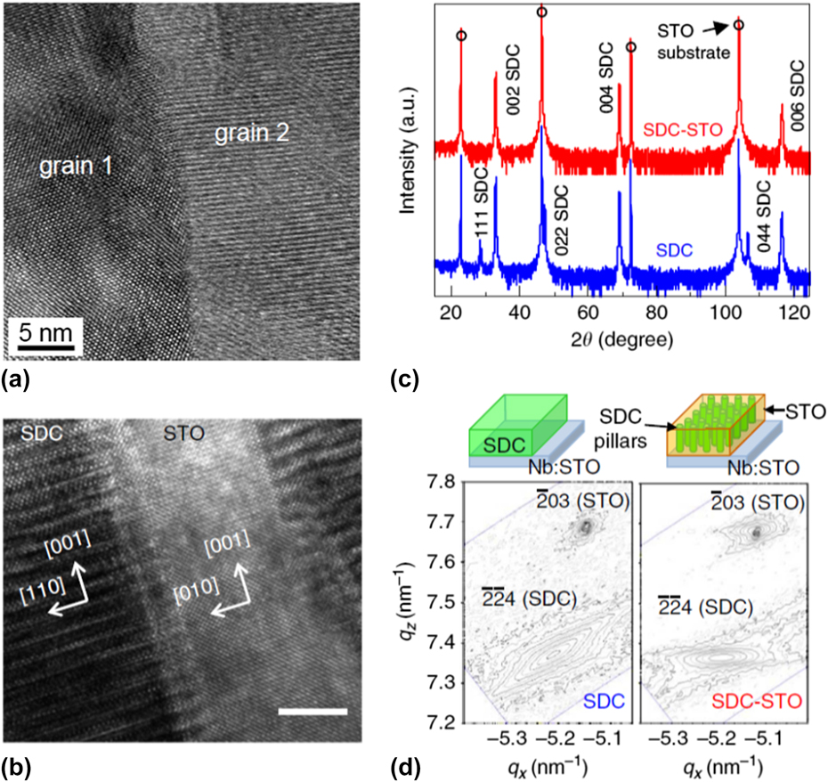
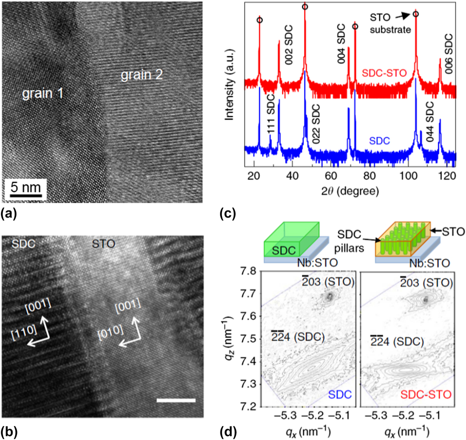
One specific example is the growth of Sm-doped CeO2 (SDC)–SrTiO3 (STO) nanocomposite films on Nb-doped STO (001) substrates compared with the single phase SDC films. Reference Yang, Lee, Jian, Zhang, Jia, Wang, Noh, Kalinin and MacManus-Driscoll53 As shown in Fig. 1(a), polycrystalline films with grains with different growth directions can be observed for the single phase SDC plain film. This is because SDC exhibits a fluorite structure, which is not compatible with the perovskite structure of the Nb-STO substrate. However, unlike the polycrystalline SDC single phase film, much better epitaxial quality can be achieved for SDC if it is grown with a secondary phase of STO in the film to form a VAN structure. As shown in Fig. 1(b), both SDC and STO grow epitaxially, with very abrupt vertical interfaces. The θ–2θ XRD results further confirm the epitaxial quality of the films, as shown in Fig. 1(c). Only SDC (00l) peaks are observed in the SDC–STO VAN film, while extra peaks of SDC (111), (022), and (044) appear in the SDC single phase film. The reciprocal space maps (RSM) of both samples also confirm the poor growth of SDC single phase films while the SDC–STO VAN film presents a very narrow SDC peak along the reciprocal space q z axis (∼5.42–5.44 Å). All these results indicate SDC has much better epitaxial quality with surrounding STO matrix compared to the single phase film, which leads to an order of magnitude enhanced ionic conduction.
High-resolution TEM image of (a) SDC plain film and (b) vertical SDC–STO interfaces in cross-sectional view. Scale bar, 10 nm. (c) Out-of-plane epitaxial relationship investigation in θ–2θ scan using X-ray diffraction. (d) RSM about the (203) STO substrate for a plain SDC film (left) and a SDC–STO nanoscaffold film (right) (Ref. Reference Yang, Lee, Jian, Zhang, Jia, Wang, Noh, Kalinin and MacManus-Driscoll53).
Another representative example is yttria-stabilized ZrO2 (YSZ) plain films, compared to YSZ–STO/SDC–STO deposited on Nb-STO substrates. Reference Lee and MacManus-Driscoll31,Reference Lee, Zhang, Khatkhatay, Wang, Jia and MacManus-Driscoll54 The large lattice mismatch of 7.5% between YSZ (with 45° rotation) and Nb-STO substrate, as well as the different structure hinders the epitaxial growth of thick YSZ film on a Nb-STO substrate. However, a YSZ–STO 2-phase nanocomposite grown on a SDC–STO buffered substrate exhibits much better epitaxial quality and has an ionic conductivity an order of magnitude higher. This occurs because SDC–STO has almost perfect epitaxial quality on STO, arising from the presence of the STO in the film. The SDC component of the film is stabilized by vertical epitaxy with the STO in the film, owing to the small lattice mismatch between SDC and STO (1.7%), despite the structures being very different. The VAN YSZ–STO film shows better epitaxial quality on the SDC–STO buffered substrate, than the YSZ–STO film does on an unbuffered STO. This is because YSZ can readily nucleate on the SDC regions in the nanocomposite buffer since YSZ and SDC have the same fluorite structure. Hence, the relatively large lattice mismatch of 5.5% between YSZ and SDC is less important. In the double composite structure, a two order of magnitude increase in ionic conductivity results compared to YSZ plain films. Overall, YSZ–STO VAN films, with the SDC–STO template obtain much better epitaxial quality than YSZ single phase films.
B. Nanocomposite-substrate in-plane lattice matching: choosing the appropriate substrate and film composition
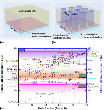
Based on the above examples, it is obvious that the VAN platform facilitates the epitaxial growth of 2-phase nanocomposites with large lattice or structural mismatch with the underlying substrates in which otherwise the epitaxial growth could not be achieved or could be very difficult to achieve in the single phase film form. In single phase films, as illustrated in Fig. 2(a), the lateral interface is the film–substrate interface. Uniform in-plane lattice strain is obtained across this lateral interface. However, in the case of the VAN films in Fig. 2(b) (phase A of nanopillars in matrix B form), the heterointerface between the film and the substrate is a mixed interface area of A pillars with the substrate and B matrix with substrate. Thus, the overall strain between the film and the substrate is the sum of the strains from both A and B interfaces with the substrate, which is largely determined by the phase compositions (i.e., A:B atomic or molar ratio).
(a) A single-phase film shows lattice misfit induced strain at the film–substrate interface; (b) VAN film shows lattice misfit-induced strain at the pillar–substrate interface; (c) in-plane lattice constants (left axis: phase A; right axis: phase B) as a function of composition ratio for phase A. The slanted dashed lines connecting phase A and phase B demonstrate the tuned range of in-plane lattice constant for each particular VAN system, which can be used for selecting suitable substrates. The straight solid lines represent in-plane lattice constants of the most popular substrates (MgO, STO, and LAO). The composition acronyms correspond to compositions shown in the left or right hand axes.

As illustrated in Fig. 2(c), different VAN systems generate different average in-plane strain states on the various common substrates. An ideal situation is that the A and B phases present opposite signs of strain state with the underlying substrate and thus the two phases compensate the large strain with the substrate and the sum of the in-plane strain can be minimized. For example, phase A with an in-plane tensile strain and phase B with an in-plane compressive strain could result in a net zero strain in-plane with a properly designed A:B ratio. To illustrate the tunable in-plane lattice parameter based on the rule of mixtures between A and B phases, Fig. 2(c) plots the lattice parameters of selected A phases (left vertical axis) and the lattice parameters of the possible B lattices (right vertical axis) versus the A:B ratios along the horizontal axis. For the same VAN systems, by tuning the molar ratio of each phase the average in-plane lattice matching can be changed. The lines connecting the different A (left) and B phases (right) illustrate the rule-of-mixtures in-plane lattice parameters depending on the A and B ratios, which is therefore an estimation of the average nanocomposite in-plane lattice parameters.
The three horizontal solid lines represent the lattice parameters of the most popular oxide substrates, such as MgO, STO, and LAO. The three lines intersect with many of the A:B mixture lattice parameter lines, the intersection points representing zero average in-plane strain between film and substrate. Hence, by tuning the ratio of phase A and phase B, it is possible to adjust the VAN in-plane lattice parameters to lattice match on these 3 different substrates. For example, (Ba,Sr)TiO3 (BSTO) on the left axis can form VAN with Sm2O3 (SmO) on the right (an orange dashed line). The line intersects with STO and LAO lines at the molar ratio of 0.2 and 0.5, respectively, suggesting the BSTO:SmO VAN system could grow on STO or LAO substrates with almost perfect average in-plane lattice matching at these A:B ratios. Figure 2(c) gives a reasonable guide for selecting appropriate substrates to give minimal average in-plane strain for specific VAN compositions and composition ratios.
Many previously reported systems with different phase ratios have been marked out in Fig. 2(c). For example, a perfect average in-plane matching between BTO:CeO2 50:50 (0.5 molar ratio) VAN and the STO substrate has been demonstrated and plotted as a dark orange dot on the orange colored STO line. As seen from Fig. 2(c), a large number of the reported VAN cases focus on 50:50 ratio, although only a few of these compositions match well with both STO and LAO substrates, many cases having an average compressive in-plane strain in the film (lower than the substrate line) or tensile in-plane strain (higher than the substrate line). The following section discusses some of the specific examples.
C. In-plane matching and alignment of VAN film on substrate
Figure 2(c) assumes cube-on-cube epitaxial matching, where the vertical axes plot the lattice parameters of phase A (left vertical axis) and phase B (right vertical axis). However, there are other types of in-plane matching relationships between the film and the substrate, such as 45° or other in-plane rotations of the film with respect to the substrate. In this case, the matching distances after the in-plane rotation are also plotted in Fig. 2(c). For example, CeO2 has a typical 45° in-plane rotation which results in a matching distance of
 ${a \mathord{\left/ {\vphantom {a {\sqrt 2 }}} \right. \kern-\nulldelimiterspace} {\sqrt 2 }}$
, as plotted on the right vertical axis for phase B. More detailed case studies are provided for the different in-plane rotation cases in Sec. II.C.1–II.C.3 below.
1. Cube-on-cube matching with no in-plane rotation
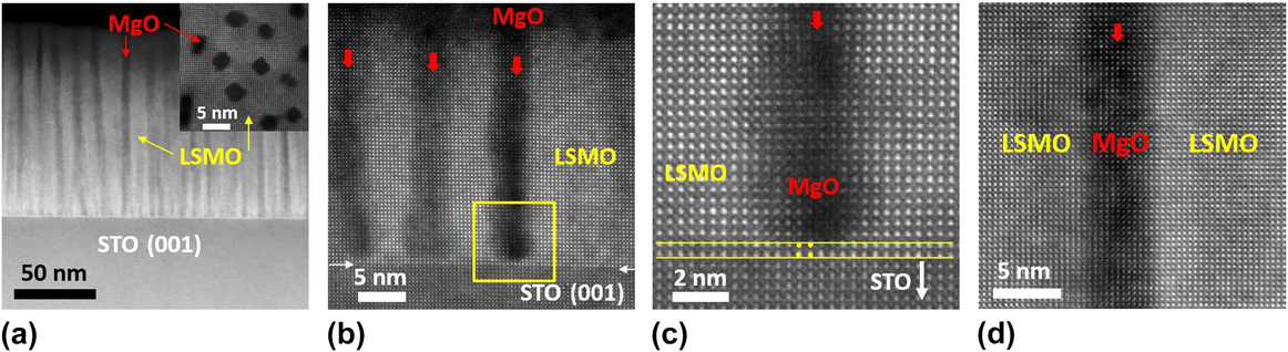
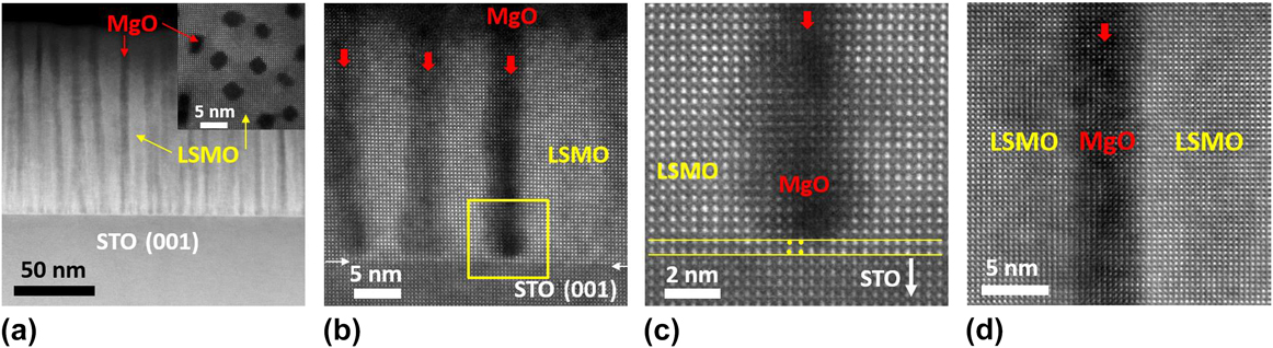
Most of the reported film-substrate lattice matching arises from cube-on-cube matching where there is no in-plane rotation of the film on the substrate. Reference Aimon, Choi, Sun, Kim and Ross61–Reference Comes, Liu, Khokhlov, Kasica, Lu and Wolf67 As illustrated in Fig. 2(c), the most popular substrates are MgO (8.12 Å/2 = 4.06 Å), STO (3.905 Å), and LAO (3.821 Å). A large number of oxides fall into these lattice parameter regions. This is also the simplest matching relation. Based on the sum of the strain of the VAN systems, there are three possible strain scenarios (in-plain), such as both tensile, both compressive, and one tensile-one compressive. For example, as illustrated in Fig. 3(c), many films grown on MgO will be under tensile strain for both phases in the VAN film, as MgO has a larger lattice parameter than many oxide perovskite films of interest. BFO–CFO, PTO–CFO, BFO–Fe3O4 on STO or LAO also present tensile strain similarly. Ideally, to grow highly epitaxial nanocomposite thin films, it would be beneficial to minimize the average in-plane strain. Hence, if one phase in the film is in compression, the other phase should be in tension. LSMO–MgO on STO is a typical example. Reference Chen, Hu, Lu, Yang, Zhang, Li, Ahmed, Enriquez, Weigand, Su, Wang, Zhu, MacManus-Driscoll, Chen, Yarotski and Jia68 As shown in Fig. 3, MgO nanopillars with size of ∼4 nm are embedded in LSMO matrix on the STO substrate. High-resolution TEM images show very high epitaxial quality of LSMO and MgO in both the in-plane and out-of-plane directions, which demonstrates the excellent quality of the entire nanocomposite film.
(a) Cross-section STEM image showing the alternating growth of LSMO (white) and MgO vertical nanoscaffolds (dark) on STO (001) substrates. Inset: plan-view STEM image of the LSMO:MgO film; (b) high-resolution STEM image showing the vertical MgO nanoscaffolds in LSMO phase; (c) zoomed-in yellow box area in (b) showing the film-substrate interface; (d) high-resolution STEM image showing the vertical interface between the MgO and LSMO phase (Ref. Reference Zhao, Li, Lee, Choi, Liang, Zhang, Tang, Wang, Jia, MacManus-Driscoll and Yang64).
2. Matching with 45° in-plane rotations
Lattice matching with 45° rotation always occurs when there is large lattice mismatch between film and substrate. An example is the growth of CeO2 or Sm2O3 on SrTiO3.
Reference MacManus-Driscoll, Zerrer, Wang, Yang, Yoon, Fouchet, Yu, Blamire and Jia13,Reference Khatkhatay, Chen, Lee, Zhang, Abdel-Raziq and Wang69–Reference Chen, Bi, Hazariwala, Zhang, Su, Chen, Jia, MacManus-Driscoll and Wang77
The lattice parameter of CeO2 is
 ${a_{{\rm{Ce}}{{\rm{O}}_{\rm{2}}}}}$
= 5.411 Å. After 45° rotation,
 $\sqrt 2 {a_{{\rm{Ce}}{{\rm{O}}_{\rm{2}}}}}$
= 7.652 Å, which is close to 2a
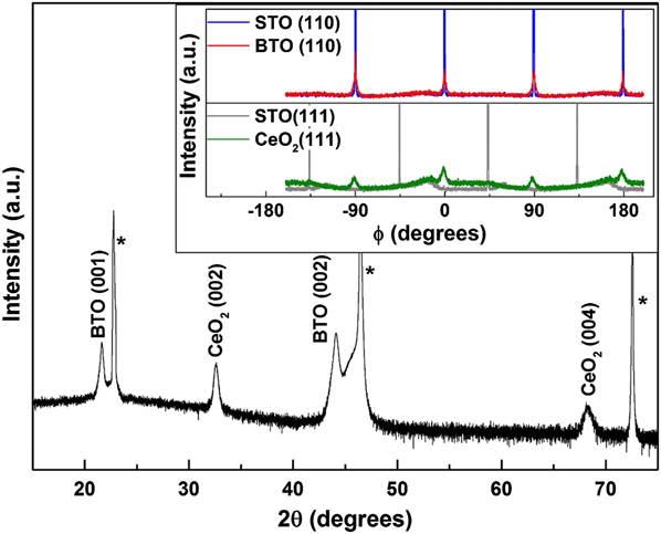
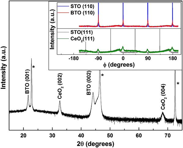
STO = 2 × 3.905 Å = 7.81 Å. For example, BTO–CeO2 VAN grown on STO substrates, with out-of-plane (001) preferred growth of both BTO and CeO2 from θ–2θ scan (Fig. 4). As shown from the φ scans inset in Fig. 4, BTO grows on STO with cube-on-cube in-plane matching, while CeO2 exhibits 45° in-plane rotations on STO. Sm2O3 is another example of the 45° rotation case which allows good lattice matching between Sm2O3 (10.92/4 ×
 $\sqrt 2$
= 3.86 Å) with STO (3.905 Å).
Reference MacManus-Driscoll, Zerrer, Wang, Yang, Yoon, Fouchet, Yu, Blamire and Jia13,Reference Lee, Harrington, Kursumovic, Defay, Wang, Bi, Tsai, Yan, Jia and MacManus-Driscoll75,Reference Lee, Sangle, Lu, Chen, Zhang, Lee, Wang, Jia and MacManus-Driscoll76
Both cases present perfect average lattice matching of the VAN film with STO and LAO substrates as indicated in Fig. 2(c).
XRD θ–2θ scan of the for BTO–CeO2 films grown on STO. The inset shows the φ scan of the BTO (110) plane relative to the STO (110) plane and the CeO2 (111) plane relative to the STO (111) plane (Ref. Reference Zhu, Tsai, Wang, Kwon, Wang, Varanasi, Burke, Brunke and Barnes65).
3. Matching for rotations other than 0° or 45° and DME
The last type of in-plane matching occurs when the nonperovskite phase in the VAN film has a nonperovskite structure and large lattice mismatch, e.g., for the hexagonal lattice structure. ZnO is one of the most widely studied cases because of its hexagonal closed packed structure.
Reference Chen, Bi, Tsai, Lee, Su, Zhang, Jia, MacManus-Driscoll and Wang24,Reference Kang, Wang, MacManus-Driscoll, Li, Jia, Mihut and Betts26,Reference Chang, Liu, Tra, Chen, Wei, Tzeng, Zhu, Kuo, Hsieh, Lin, Zhan, Luo, Lin, He, Wu and Chu78,Reference Chen, Zhang, Khatkhatay, Su, Tsai, Chen, Jia, MacManus-Driscoll and Wang79
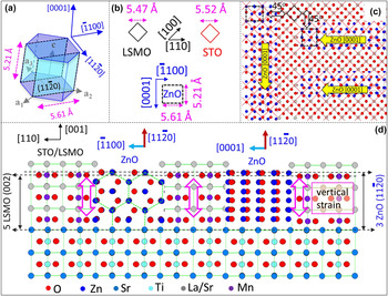
For example, LSMO–ZnO on STO is a unique case in this category. The crystal structure of ZnO is shown in Fig. 5(a), with the
 $\left( {11\bar 20} \right)$
and
 $\left( {\bar 1\bar 120} \right)$
planes marked out. As we can see, the
 $\left( {11\bar 20} \right)$
plane can be treated as rectangles with edge length of 5.21 Å and 5.61 Å. Interestingly, this rectangle can match well with STO after a 45° rotation, as revealed in Fig. 5(b). Therefore, the in-plane direction of ZnO will be [0001], as illustrated in the schematic atomic arrangements of LSMO–ZnO on STO in Fig. 5(c). Two growth possibilities for ZnO are demonstrated, one is ZnO along [0001] direction, which results in the formation of rectangular nanodomains. The other is the growth of ZnO [0001] along either STO [110] or
 $\left[ {1\bar 11} \right]$
directions, which leads to an orthogonal arrangement of the nanorectangles.
(a) Crystal structure of hexagonal ZnO. (b) In-plane matching between ZnO, LSMO, and STO lattice. (c) Atomic arrangement of in-plane lattice matchings (Ref. Reference Lee, Harrington, Kursumovic, Defay, Wang, Bi, Tsai, Yan, Jia and MacManus-Driscoll75).

In some cases, however, none of the above discussed lattice matching conditions occurs and then it is possible that DME takes place. DME typically occurs when the lattice mismatch is too large (typically f > 7%) to satisfy LME. In addition, high interfacial energy from dissimilar crystal structures is also a critical factor for DME. Thus both the structural mismatch and lattice mismatch could result in DME for minimizing the overall interfacial energy in the system. For the case of DME, an integer number (m) of film lattices match with an integer number (n) of substrate lattices to allow an overall reduced film/substrate strain. The DME growth model has been observed in various material systems, such as 6 GaN–5 Si (111) matching, 3 TiN–4 Si (100) matching, etc., Reference Narayan and Larson80–Reference Wang, Tiwari, Kvit, Zhang and Narayan82 but mostly in single phase thin films. The complexity of DME in VAN systems for in-plane matching is that the DME matching relations could be different for phase A/substrate and phase B/substrate, which result in various misfit dislocation spacing for domain A and domain B. There is no report so far on the direct TEM observation of in-plane DME cases in VAN systems, possibly due to the small domain sizes and the complex imaging conditions required.
III. PART II: VERTICAL OUT-OF-PLANE LATTICE MATCHING: PICK THE APPROPRIATE VAN SYSTEMS
Having discussed in-plane strain and epitaxy between VAN films and different common single crystal substrates, we now focus our discussion of the vertical out-of-plane epitaxy which occurs between the two phases in the VAN films. In-plane lattice matching of the film to substrate is important for initiating epitaxial film growth. Once the film has begun to grow and assemble into two distinct phases, the vertical out-of-plane pillar-matrix heteroepitaxial interface [Fig. 6(a)] plays the most important role in determining the growth, in particular the level of crystallinity and strain throughout the whole thickness of the film.
(a) VAN systems with lattice misfit induced strain along the phase A-phase B vertical interface. Note the pillar phase is typically the minority phase; (b) out-of-plane 1:1 lattice epitaxial matching and n:m domain matching epitaxial (DME) matching for reported VAN systems. Here, the underlined systems are known DME systems and the nonunderlined ones are assumed to be LME ones, although it is possible that for several of these systems there are DME, but the type of epitaxy has simply not been experimentally studied. For the known DME cases, the lattice parameters are determined by matching integral numbers of lattices, e.g., for 7 LSMO (001):5 CeO2 (001), the reduced matching relation is LSMO (001):5/7 CeO2 (001), thus the plotted matching distance for d
LSMO is 3.9 Å (d
1), while the plotted matching distance
 ${d_{{\rm{Ce}}{{\rm{O}}_2}}}$
= 5.41 Å × 5/7 = 3.86 Å (d
2).

A huge pillar-matrix interfacial area can be created, depending on the pillar size and density and the film thickness, Reference MacManus-Driscoll, Zerrer, Wang, Yang, Yoon, Fouchet, Yu, Blamire and Jia13 which strongly influences the overall vertical strain level and physical properties accordingly. Reference Bi, Lee, Yang, Jia, MacManus-Driscoll and Wang83 Similar to the in-plane film-substrate matching, the vertical out-of-plane matching between phase A and phase B also involves LME or DME, depending on the lattice mismatch between A and B. Some reported systems for both types of epitaxy modes have been summarized in Fig. 6(b). As discussed in Section C3, small lattice mismatch or low interfacial energy will result in LME. Some of the selected cases are plotted and labeled without underlines in Fig. 6(b), such as BTO–CFO. Larger mismatch cases result in DME (typically f > 7%), which are underlined in Fig. 6(b). For example, for 7 LSMO (001)–5 CeO2 (001), of perovskite and fluorite structures, 7 LSMO unit cells match with 5 CeO2 unit cells. It is noted that the LME cases are typically far away from the 1:1 matching line marked as a diagonal red line in Fig. 6(b), which indicates the vertical strain between A and B in these cases are relatively large. The cases of DME are typically close to the 1:1 matching line which results in less effective vertical strain between phases A and B. It shall be noted that the LME cases listed here may, in fact, be DME cases but they have simply not been reported experimentally. Several representative examples are given below to further demonstrate different matching relations.
First, the most straightforward condition occurs when the two phases have the same structure with similar lattice parameters. For this condition, one achieves one-by-one epitaxial matching, giving semicoherent epitaxial growth. Let’s take LSMO–BFO system grown on STO as an example. Reference Zhang, Chen, Jian, Zhu, Chen, Lu, Jia, MacManus-Driscoll, Zhang and Wang32 Both LSMO and BFO have the same perovskite structure (although different overall symmetries). Since the structures are similar, the lattice parameters are quite close: LSMO, BFO, and STO have lattice parameters of 3.87 Å, 3.962 Å, and 3.905 Å, respectively. Good quality epitaxial films are anticipated in both the in-plane and out-of-plane directions. Of course, there may be some cation intermixing across the individual phases, but this effect is expected to be minimized if cation sizes are quite different and if the overall strain state of the film is lower when mixing does not occur.
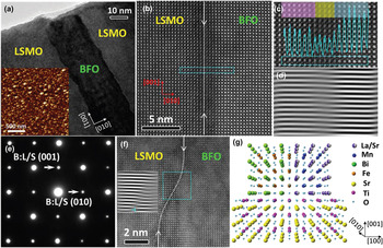
Figure 7(a) exhibits cross-sectional TEM image of LSMO0.75:BFO0.25 film, BFO nanopillars embedded into LSMO matrix can be seen. The high resolution TEM images of the interface area in Figs. 7(b) and 7(c) present sharp and clean LSMO–BFO interfaces, which indicates excellent epitaxial quality of the film. Figure 7(d) shows the fast Fourier transform (FFT) image of the area in Fig. 7(c), with exact one-to-one lattice matching between LSMO and BFO. At the vertical LSMO/BFO interface, an ultrathin dark region results because of the strain arising from lattice mismatch between LSMO and BFO. However, no dislocations have been observed. It is also possible that no dislocation observed for this case is due to the limited TEM imaging area. The selected area electron diffraction (SAED) pattern in Fig. 7(e) further confirms the perfect epitaxial quality of the film. However, the film quality is deteriorated by tuning the composition ratio of the two phases. Indeed, a curved interface with dislocations is seen for a LSMO0.33:BFO0.67 sample, as illustrated in Fig. 7(f). The different interface compared to the perfect vertical interface for the LSMO0.33:BFO0.67, may be explained by two factors, (i) average in-plane strain effects or (ii) structural stability effects. For (i) which takes into account strain effects, referring back to Fig. 2(c), for LSMO:BFO ratio of 0.5:0.5 (LSMO0.5:BFO0.5), there is no or very small average in-plane strain with the STO substrate, whereas for LSMO0.33:BFO0.67, there is average in-plane strain of 0.6% and LSMO0.75:BFO0.25 has an average in-plane strain of 0.3%. Hence, the interface curvature may result to minimize the larger strain in the LSMO0.33:BFO0.67 case. For (ii) which takes into account structural stability effects, there is a larger proportion of BFO in the LSMO0.33:BFO0.67 film, and hence less LSMO to vertically confine and constrain the BFO to a pseudo-cubic form. Since BFO is not a cubic perovskite, but rather a distorted perovskite, the curved interface may result to minimize strain as the BFO tries to relax to its distorted perovskite form.
(a) Cross-sectional TEM image of a LSMO0.75BFO0.25 (L0.75B0.25) VAN film showing a BFO pillar embedded in a LSMO matrix. The inset shows the corresponding top-view AFM image. (b) High-resolution STEM image of the vertical heterointerface between LSMO and BFO. (c) Enlarged view of the atomic lattice across the heterointerface. The intensity line profile is inserted along the marked rectangular region. (d) FFT image of (c) showing the coherent one-to-one lattice matching without any dislocations. (e) Corresponding SAED pattern showing the high epitaxial quality of a L0.75B0.25 film. (f) High-resolution STEM image of the heterointerface in a L0.33B0.67 film, showing increased interface roughness. The inset shows the FFT image of the marked region identifying dislocations. (g) Crystallographic model of the L1−x B x VAN films (Ref. Reference Zhang, Chen, Jian, Zhu, Chen, Lu, Jia, MacManus-Driscoll, Zhang and Wang32).

Figure 7(g) is the schematic atomic model to show the one-on-one crystallographic relationships of LSMO–BFO on STO. Owing to the formation of the perfect vertical interface, strong magnetic exchange coupling and the perpendicular exchange bias (PEB) effect can be achieved in this interesting structure.
Besides standard vertical LME, vertical DME also plays an important role in VAN systems to give high epitaxial quality. As for the case of the interface with the substrate, DME occurs in systems having different crystal structures and large lattice mismatch, hence where the interfacial energy between the structures is high. Thus, STO (perovskite)–Sm2O3 (bixbyite) is a typical example to show vertical DME.
Reference Lee, Sangle, Lu, Chen, Zhang, Lee, Wang, Jia and MacManus-Driscoll76
Fig. 8(a) shows a high resolution HAADF STEM image in the interface area of STO and Sm2O3, which presents a very sharp and clean vertical interface. A schematic crystallographic model is built in Fig. 8(b). 10 Sm planes match with 7 SrO planes. This is because 10 × a
SmO (004)=7 × a
STO (001)=27 Å, and this 10:7 domain matching is energetically favorable due to the significantly reduced strain by DME. DME also takes place in various CeO2(fluorite)/perovskite-based VAN systems. For example, 5 CeO2 (002)–7 LSMO (002) is obtained by alternating 2 CeO2 (002)–3 LSMO (002) and 3 CeO2 (002)–4 LSMO (002) in LSMO–CeO2 VAN system.
Reference Chen, Bi, Hazariwala, Zhang, Su, Chen, Jia, MacManus-Driscoll and Wang77
The last well studied case is the previously discussed ZnO related system.
Reference Chang, Liu, Tra, Chen, Wei, Tzeng, Zhu, Kuo, Hsieh, Lin, Zhan, Luo, Lin, He, Wu and Chu78
Fig. 8(c) presents the schematic atomic model showing the vertical interface of LSMO–ZnO. Interestingly, five LSMO (002) match very well with three ZnO
 $\left( {11\bar 20} \right)$
, which produces a residual vertical strain of only 0.5% in LSMO phase.
(a) High-resolution HAADF image of vertical interface of SrTiO3 matrix and Sm2O3 nanocolumn in cross-sectional-view; (b) crystallographic modeling of vertical interface between SrTiO3 and Sm2O3 (Ref. Reference Huang, Fan, Wang, Chen, Tsai, Li and Wang72); (c) atomic arrangement of out-of-plane lattice matching between LSMO (002) planes and ZnO
 $\left( {11\bar 20} \right)$
planes in the STO
 $\left[ {1\bar 10} \right]$
zone axis (Ref. Reference Lee, Harrington, Kursumovic, Defay, Wang, Bi, Tsai, Yan, Jia and MacManus-Driscoll75).

IV. SUMMARY AND OUTLOOK
Overall, VAN structures provide unique advantages over conventional single phase films, such as the ability to maintain high levels of uniform vertical strain throughout the entire film thickness, and large interfacial areas for interfacial coupling and multi-functionalities. With their enormous potential in functional materials design, there is much work needed in both the development of VAN-based multifunctional devices as well in their fundamental strain-controlled growth mechanism(s). In terms of future research directions, selected focus directions are: (1) VAN in-plane strain coupling between two phases and their impact on in-plane lattice matching and overall growth morphologies. Figure 2(c) provides a guideline to choose a matching substrate and design VAN systems with different phase ratios for the matching substrate. This compensated in-plane matching of both phases with the underlying substrate allows the growth of high quality epitaxial films of a phase which, on its own, has large lattice mismatch with the substrate, and hence would not grow with high quality without the use of a VAN film to lower the average in-plane strain. In many cases, some application-preferred substrates, such as Si, should be further considered and tested to replace the single-crystal substrates. Since, after the initial nucleation stage VAN films have synergistic stabilization of epitaxy between the phases in the film, they may grow more easily on Si. Indeed, there are already promising results shown for VAN film growth on Si. Reference Zhang, Li, Lu, Fan, Su, Khatkhatay, Chen, Jia, Zhang, MacManus-Driscoll and Wang25 (2) Owing to the large pool of oxides in nature, there are still plenty of VAN systems to be explored and exploited for inducing multifunctional properties. LME and DME, for both in-plane and out-of-plane matching should be considered while designing VAN systems [Fig. 6(b)]. In particular, it is important to exploit the fact the DME enables more uniform films to be grown beyond a lower critical thickness for strain relaxation. (3) 2D interfaces in VAN films should be studied much more closely. While recent work in STO-based VAN films have shown fascinating tunable electronic and ionic effects, Reference Lee, Sangle, Lu, Chen, Zhang, Lee, Wang, Jia and MacManus-Driscoll76,Reference Cho, Yun, Tappernzhofen, Kursumovic, Lee, Lu, Jia, Fan, Jian, Wang, Hofmann and MacManus-Driscoll84 2D effects have been little explored. However, VAN films provide the ideal systems for creating and engineering large area 2D interfaces. Hence, there is huge promise for creating emergent 2D effects over very large areas, in films made very simply. Furthermore, since VAN interfaces self-assemble, and also grow much more slowly compared to ‘forced’, rapidly grown interfaces in standard planar heterostructures, there is the chance to create less defective interfaces.
ACKNOWLEDGMENT
The work is funded by the U.S. National Science Foundation (DMR-1643911 for VAN thin film growth and DMR-1565822 for high resolution TEM/STEM work). JLM-D acknowledges support from EPSRC grants, EP/K035282/1 and EP/N004272/1 and the Leverhulme grant RPG-2015-017.