

DISCUSSION POINTS
• Gallium nitride is currently the wide band gap semiconductor material from which almost all commercial LEDs for solid-state lighting are manufactured but in the future other promising materials, such as zinc oxide (ZnO), are also likely to play a leading role.
• With further developments in LED technology, leading to cheaper luminaires, perhaps based on gallium nitride-on-silicon material, LED lamps will largely replace tungsten incandescent bulbs in the years to come.
Introduction
Artificial, electrically driven lighting accounts for a very significant portion of humankind's total energy usage on this planet. Since the advent of electrical lighting in the late 19th century, illuminating our homes, workplaces, and outdoor spaces has been consuming an increasingly large proportion of electric power. During this time, other electrical devices and appliances have gained in efficiency and benefited from the solid-state electronics revolution. However, until quite recently, the mainstream electric lighting has remained firmly in the vacuum tube era with devices based on gas-filled incandescent and fluorescent bulbs illuminating our homes and workplaces. It is only over the last two decades that solid-state light generating devices in the form of light-emitting diodes (LEDs) have become available as an alternative for lighting up living spaces.Reference Rahman1,Reference Fred Schubert, Kyu Kim, Luo and Xi2 This review takes a look at their development, current status, and future prospects. After a brief historical introduction, the development and structure of the blue LED at the heart of all white LEDs are examined. This is followed by a description of various techniques that have been explored to extract more light from LED chips. Such techniques make LEDs brighter without increasing their energy consumption and thus enhance their attractiveness as energy-efficient light sources. The relatively recent development of a gallium nitride-on-silicon material for low cost, high performance LEDs is examined next, followed by a look at the phosphor technology for white LEDs. The societal impact of LED lighting is then described with this review ending by examining the still distant goal of making LEDs out of zinc oxide (ZnO) as a challenge facing the solid-state electronic materials community. The drive to develop ever better LEDs comes from our desire to have the most energy efficient means of space illumination. LEDs excel in this attribute but, additionally, also offer many other benefits such as environmental sustainability, low maintenance requirements, and long lifetimes. Although these devices are now well-established as a serious alternative to other types of electric lighting, they are still being rapidly improved. Material science reigns supreme in this quest as many of these developments hinge on finding the best materials, material combinations, and device fabrication technologies for constructing high efficiency light-emitting devices.
Historical context
That lighting represents an inefficient use of electric power dawned very early on and efforts were directed toward developing more efficient light sources. Tungsten filament-based incandescent lamps initially had efficiencies as low as 2% but were greatly improved in later years through the incorporation of such technologies as inert gas filling and double-coiled filaments, which resulted in several fold increase in their efficiency to figures of around 8% today. The development of a tungsten-halogen lamp, incorporating the halogen regeneration technology, in the 1950s was a significant step toward further improving the nearly century-old incandescent lamp technology. Filling bulbs up with small amounts of halogens allows the lamp filament to operate at much higher temperatures without the risk of shortening its operating life. Higher filament temperatures increase the efficiency of electrical-to-light energy conversion and the tungsten-halogen lamps boast efficiencies of as high as 32%. It is very likely that the incandescent lamps have reached the pinnacle of achievable efficiency and further improvements do not seem possible. Moving to a radically different technology is the only way to further increase the efficiency of lighting devices.
At about the same time that tungsten-halogen lamps made their first commercial appearance, another lighting technology – this one being based on electrical discharge in gases at low pressure – was also being commercialized. The fluorescent lamp, developed at General Electric, was a very different kind of light source – based as it was on light emission from excited gas molecules energized by an electric discharge. In this lamp, mercury atoms are excited by collisions with energetic argon atoms, which, in turn, are fed energy from an electric discharge. The excited mercury atoms emit ultraviolet radiation as they shed their excess energy and relax to the ground state. The ultraviolet radiation is converted to visible light as it strikes a fluorescent coating on the inner wall of the lamp. Due to the high efficiencies of the atomic radiation emission process and the fluorescent wave length conversion, the fluorescent lamp is a relatively efficient converter of electrical energy to light. Modern mercury vapor-filled fluorescent lamps have typical efficiencies in the range of 60–65%.
Just like its predecessor, the tungsten filament incandescent lamp, the fluorescent lamps have also reached the zenith of perfection and significant further improvements in either their lifetime or energy efficiency are hardly likely. To achieve higher efficiency figures for electric lighting, a radically different technology is required. Fortunately, such a technology has been in existence for a long time but was not considered suitable for space illumination applications until two decades ago. During the early 1990s, LEDs were still tiny solid-state light emitters, used for indicator applications in electrical and electronic systems. At that time, they were still much the same in physical form as in the 1960s – the decade of their invention. This began to change in the later years of 1990s as higher-powered devices were developed with bigger chips. The main problem with such devices was the necessity of removing heat as efficiently as possible so that the diodes did not overheat and destroy themselves. Once suitable device packaging technologies were developed, this became a reality. A concomitant development was the realization that blue LEDs can be used to generate white light by the same technique that enables fluorescent lamps i.e., phosphor-based wave length down-conversion. The initial trials were quite successful and thus the first lighting-quality white LEDs were born. Of course, central to this development was the invention of the blue LED itself which was the last solid-state visible color emitter to be developed.
The blue LED
The blue-to-violet region of the visible spectrum spans the wavelengths from around 480 nm down to 400 nm. To generate light in this region requires the use of relatively wide band gap semiconductors. There are several semiconductors with suitable band gaps available but not all can be used for making LEDs. The other attributes needed for practical blue LED materials include qualities such as a direct band gap with vertical (nearly zero momentum) transition between conduction and valence bands, wide availability, easy processing, and, perhaps the most important, straightforward doping characteristic to obtain both n- and p-type materials. The last requirement has been the bane of most prospective blue LED materials. Several oxide, carbide, and nitride materials were identified early on as likely candidates for making blue light-emitters but turning them into active light-emitting pn-junction diodes proved far from simple. The main difficulty arises from the fact that wide band gap semiconductors are often hard to dope so as to produce a stable, high conductivity material. An efficient LED cannot be constructed unless a practical route can be found to produce robust n- and p-type materials with low bulk and contact resistivities. Thus, while silicon carbide (SiC), ZnO, and gallium nitride (GaN) were all deemed suitable for making blue LEDs, suitable doping techniques eluded early researchers for many years. This is a commonly encountered difficulty with all wide band materials. The situation changed dramatically when Shuji Nakamura – a young researcher at Nichia Corporation in Japan – developed a practical and reliable method for producing p-type GaN. n-type GaN was already available but creating hole-rich material had proved problematic for many years. As described further below, this development led to the fabrication of the first GaN blue LEDs (and later also to the creation of blue–violet GaN diode lasers).Reference Johnstone3 While GaN has remained the mainstay of blue LEDs, commercial devices have also been made from SiC – a much more expensive material. The brightness of blue (and white) LEDs has climbed over the years so that now we have multiwatt single chip LEDs as well as much higher power multichip chip-on-board devices, commercially available from a number of manufacturers. ZnO has so far resisted attempts toward reliable p-type doping and thus research on this material, as described later in this article, is still in a learning phase.
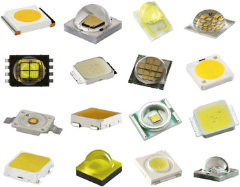
GaN and associated III-nitride alloys, such as InGaN and AlGaN, have been used for the commercial manufacture of both LEDs and lasers for many years now. The wide band gap of III-nitrides allows the manufacture of devices emitting short wave length radiation ranging from the green–blue part of the visible spectrum to well inside the UV region. The exact wave length can be tuned by changing either the width of the quantum wells used in the active layers of the device (quantum tuning) or the exact composition of the well material (compositional tuning). The addition of aluminum causes the emission wave length to shift to lower values (deeper into the UV) whereas the addition of indium causes it to shift toward the green region of the visible electromagnetic spectrum. The issues on material quality limit how far these transitions could be pushed in either direction. Thus, obtaining efficient deep UV LEDs from AlGaN material is still a major research goal as is the fabrication of long-life and high efficiency green LEDs from a high indium content InGaN material. Although both deep UV and green III-nitride LEDs are now commercially available, their efficiency and longevity are significantly inferior to usual blue LEDs. Their cost is also very high which severely limits their applications in cost-sensitive industrial and consumer equipment. Considerable progress has been achieved over the years in pushing out both wave length ends. At present, there is a lot more activity devoted to the development of deep UV LEDsReference Maeda and Hirayama4–Reference Zhang, Hu, Lunev, Deng, Bilenko, Katona, Shur, Gaska and Asif Khan7 from III-nitrides than that for developing true green LEDs. This is partly because other materials might eventually work for producing high efficiency green LEDs, as several materials, such as II–VI semiconductors, have shown promise in the past. At the time of this writing, the AlGaInP material system is routinely used for the manufacture of long wave length visible light LEDs (red to yellow) while the InAlGaN system is used for short wave length devices (blue and violet). Green can be approached from either end but the efficiency and lifetime of green diodes are significantly lower than those of their shorter and longer wave length counterparts.Reference Zhao, Oh, Wu, Kawaguchi, Tanaka, Fujito, Speck, DenBaars and Nakamura8 This situation is sometimes referred to as the ‘green hole’ or ‘green gap’. At present, GaN is the predominant material for the manufacture of blue, violet, near-UV, and phosphor-converted white LEDs. Metal organic chemical vapor deposition (MOCVD) is the technique predominantly used for making GaN LEDs but some experimental devices have also been made using molecular beam epitaxy.Reference Johnson, Bousquet, Hooper, Kauer, Zellweger and Heffernan9 Some commercial blue-emitting LEDs are also produced from SiC but their comparative market share is small. White LEDs for solid-state lighting are essentially blue or near-UV GaN LEDs, coated with a phosphor material. Such luminescent conversion LEDs work by converting a part of the incident pump light to yellow–orange light which in combination with the residual short wave length light appears white to the human eye. A very large range of LEDs of all colors (including white) is now commercially available (see Fig. 1) in sizes ranging from small indicator type devices to large multichip modules.Reference Taguchi10
Modern commercial LEDs are available in many different power ratings and package styles.

Before GaN LEDs (and lasers) could be developed, two major technical hurdles had to be overcome. One was the deposition of high quality GaN layers on sapphire and the other was the development of an efficient and reproducible technique for the creation of p-type material. The first problem was solved in 1986 by Isamu Akasaki and his colleagues at Nagoya University by depositing a thin layer of aluminum nitride (AlN), at low temperature, on top of a sapphire substrate before attempting the growth of GaN layersReference Amano, Sawaki, Akasaki and Toyoda11 at higher temperatures. AlN has one component (Al) that is common to the sapphire substrate (Al2O3) and one that is common to the overlying GaN (N) and thus it turns out to be a suitable epitaxial buffer material. The lattice parameter mismatch between sapphire and GaN is high at about 14% but the AlN buffer layer allows successful epitaxy of GaN and InGaN epilayers. The other major problem with the development of GaN-based devices was the unavailability of p-type GaN. Magnesium was known to be a prospective acceptor impurity in III-nitrides but researchers could not get it to occupy Ga sites so that it could provide holes in the resulting material. Once again this problem was first solved at Nagoya University by Isamu Akasaki's group by irradiating the magnesium doped GaN material with a high density electron beam.Reference Amano, Kito, Hiramatsu and Akasaki12 Later the Shuji Nakamura's group at Nichia also succeeded in producing p-type GaN by annealing Mg-doped samples in a hydrogen free ambient atmosphere.Reference Nakamura, Iwasa, Senoh and Mukai13 He is also credited with developing the two-flow MOCVD technique that uses a combination of horizontal and vertical gas flows to grow very high quality epitaxial material.Reference Nakamura14 Most of the basic problems with GaN and related binary, ternary, and quaternary III-nitrides have now been solved so that both electronic and optoelectronic devices are now routinely manufactured with high yields.
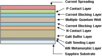
Present day GaN LEDs are multiple quantum well (MQW) devices, usually with five GaN/InGaN quantum wells sandwiched between a bottom n-type contact and a top p-type contact. The structure of a typical modern blue LED is shown in Fig. 2.
Layer structure of a modern GaN/InGaN blue LED.

The quality of anode and cathode contacts plays crucial roles in efficient LED operation. It has taken many years of hard work by several groups around the world to optimize contacts to GaN bipolar devices. Contacts to n-type GaN are now mostly formed by a Ti-containing metallization scheme, such as Ti/Ni/Au.Reference Rahman, Xu, Watson, Kumar Baid Mutha, Oxland, Johnson, Banerjee and Wasige15 Here, Ti diffuses into GaN on annealing at temperatures around 900 °C, decomposing GaN, and forming titanium nitride (TiN). This leaves nitrogen vacancies behind that act as electron donors i.e., n-type dopants, making low-contact resistance n-type contacts possible. Palladium-containing metallization schemes are usually used for making p-type contacts where the principal requirement is of a metal with a high-work function whose Fermi level could align favorably with the valence band edge of GaN.Reference Weimar, Lell, Bruderl, Bader and Harle16,Reference Lewis, Maaskant and Corbett17 Achieving low-contact resistances is extremely important for raising the efficiency of GaN LEDs as the power dissipation is the product of drive current and the forward voltage drop of the diode. The latter parameter is made up of contributions from the band gap of the quantum well used and the voltage drop due to the contact resistance, R c. The contact resistance can be calculated from the current–voltage characteristics of LEDs, using the Shockley relation:
 $$I = {I_0}\left[ {\exp \left( {{{q\left( {V - I{R_{\rm{c}}}} \right)} \mathord{\left/ {\vphantom {{q\left( {V - I{R_{\rm{c}}}} \right)} {nkT}}} \right. \kern-\nulldelimiterspace} {nkT}}} \right) - 1} \right]\quad ,$$
here I 0 is the saturation current, q is the elementary charge, n is the ideality factor, k is the Boltzmann constant, and T is the temperature in Kelvin. A contact resistance of the order of a few milliohms is desirable and is indeed achieved in modern well-fabricated devices.
All modern LEDs, in addition, feature a current spreading layer at the top that serves to distribute current evenly across the entire top face of the device. In the absence of this layer, current crowding due to the low conductivity of the top p-type GaN layer would make for an uneven light distribution and an inefficient device operation. The way around is to deposit a transparent conductor on the top (light emitting) face of the LED. The usual materials used for this purpose are either indium tin oxide (ITO) or a thin bilayer of nickel–gold. In both these cases, one has to strike the right balance between high optical transparency and high electrical conductivity, as these two attributes appear to be largely mutually exclusive. ZnO-based transparent conductive coatings have also been proposed for this function. As ZnO can be relatively easily doped n-type and has a refractive index comparable to that of GaN, so ZnO-based coatings are obviously an attractive alternative. Gallium-doped ZnO films deposited by magnetron sputtering on top of the usual ITO current spreading layers have shown improved performance when compared with devices with just the ITO top layer.Reference Sheu, Lu, Lee, Lai, Kuo and Tun18 Furthermore, the nearly matched refractive indices of GaN and ZnO make it easy to couple light from GaN epilayers into the ZnO overlayer from where it could be extracted more efficiently by texturing or faceting the ZnO layer. This is especially attractive because ZnO and GaN are isomorphic and have only a 2.2% lattice mismatch. Sun and Kwok investigated the optical properties of ZnO grown by pulsed laser deposition on sapphire and found that this material is suitable for the overgrowth of GaN for optoelectronic applications.Reference Sun and Kwok19 There is also now some interest in exploring the use of antimony-based coated mica dispersions for this application. Some experimental devices have also used a tunnel junction (TJ) approach where a TJ buried in the top p-type GaN layer serves to provide a plentiful supply of holes through a charge carrier conversion process.Reference Jeon, Song, Jang, Mo Yang, Won Hwang and Son20 Such devices have higher output luminosity but also a larger forward voltage drop because of the additional series resistance of the TJ.
To enhance the light output further, most commercial LEDs are now built by a ‘flip-chip’ process where the sapphire (used as the growth substrate) is removed by a laser lift-off (LLO) technique and the LED die is mounted on a secondary substrate (usually silicon) at the p-type end.Reference Wong, Sands and Cheung21–Reference Wong, Cho, Weber, Sands, Yu, Kruger, Wengrow and Cheung23 The light then escapes from what was previously the bottom of the device and hence the designation: flip-chip. The end bonded to the supplementary substrate then serves as a good current injector because it carries a full layer of thick metal which, incidentally, also acts as a mirror, further enhancing the light output.Reference Shchekin, Epler, Trottier, Margalith, Steigerwald, Holcomb, Martin and Krames24 Hyunsoo Kim and colleagues from Samsung Corporation and the University of Korea recently described a hybrid current spreader–reflector approach where silver-based metallic hybrid reflectors consisting of an injection part (with low p-contact resistance and intermediate reflectance) and a spreading part (with high p-contact resistance and good reflectance) were shown to improve both current injection and light reflectivity in test flip-chip devices.Reference Kim, Kim, Choi, Kim, Song, Cho, Hyeon Baik, Sone, Park and Seong25 They have reported on the fabrication of devices with an 8.9% higher power output when compared with conventional metallization devices. This leads to direct improvement in the wall plug efficiency, η = L/IV, where L is the light output power, I is the drive current, and V is the LED forward voltage drop. Another very significant advantage of removing the sapphire substrate is the relaxation of growth stress in the GaN epilayer. The biaxial compressive stress that accumulates in GaN layers grown on sapphire, with which they have a 14% lattice mismatch, can be almost completely relieved by transfer bonding to a silicon or AlN substrate followed by LLO with a deep UV excimer laser (usually a KrF laser operating at 248 nm). This process has been studied in detail by Hsu and colleagues and they have reported the dramatic improvements in both GaN epilayer stress and the deformation potential of the embedded GaN/InGaN quantum wellsReference Hsu, Pong, Li, Beechem, Graham and Liu26 through LLO processes.
Enhancing light extraction from LEDs
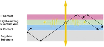
A continuing problem with III-nitride LEDs is that the high refractive index of GaN (2.4) causes light to be trapped inside LEDs made from this class of materials. This phenomenon, of course, is not unique to GaN and arises in any transparent material of high refractive index. Diamond, for instance, admits light from all angles, but once inside, the escape cone is very narrow so that the trapped light can only escape through a few well-oriented facets, giving diamond its so-called fire. Similarly, adding lead to ordinary silica glass raises its refractive index making a sample of cut lead glass sparkle. The only thing that is different from GaN optoelectronic devices is that here the light is generated in the interior of the crystal, in an active layer that typically consists of a sequence of quantum wells. Typical paths taken by light generated inside epitaxial GaN LED structuresReference David, Fujii, Sharma, McGroddy, Nakamura, DenBaars, Hu, Weisbuch and Benisty27 are shown in Fig. 3. Here, the black lines represent light that remains trapped inside the chip due to total internal reflection.
Light paths inside a LED, showing both emitted light (yellow) and trapped light (black).

Even with the provision of a reflector, only a small amount of light manages to come out of the device. This would make for extremely poor external quantum efficiency if things were left as they are. In fact, the maximum amount of light that gets extracted vertically after one reflection from the reflector is only around 16%, which is given by the expression
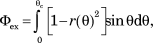 $${\Phi _{{\rm{ex}}}} = \int\limits_0^{{\theta _{\rm{c}}}} {\left[ {1 - r{{\left( \theta \right)}^2}} \right]} \sin \theta {\rm{d}}\theta \quad ,$$
here r(θ) is the Fresnel reflection coefficient and θc is the critical angle at the GaN–air interface.Reference Cho, Jang, Choi, Choi, Kim, Lee, Lee, Choe, Lee, Kim, Lee, Kim and Lee28 The overall extraction efficiency per face can also be approximated as
 $${\phi _{{\rm{ex}}}} \approx {1 \mathord{\left/ {\vphantom {1 {4{n^2}}}} \right. \kern-\nulldelimiterspace} {4{n^2}}}\quad ,$$
where n is the refractive index of the LED material. Again, it is clear that high values of n severely limit the amount of light that can be extracted from the quantum well region of LED chips.
To raise the quantum efficiency to reasonable levels, device makers have relied on various techniques such as incorporating a reflector on one face of the chip to double the amount of light that could be obtained from a LED chip or using a flip-chip approach, as described above. Yet another method for enhancing light extraction and thus increasing LED brightness is by creating a random topographic texture on the chip's surface. So roughening the otherwise planar surface of a LED chip can aid in light extraction, which was shown many years ago in the context of infrared-emitting GaAs LEDs.Reference Schnitzer, Yablonovitch, Caneau, Gmitter and Scherer29 However, later the same technique was also applied to blue-emitting GaN LEDs and it is now a standard feature of all commercial LEDs.Reference Na, Han, Kim, Lim, Kim and Park30 Random surface texturing can be produced by simply carrying out a maskless wet etching of LED surface using, for example, an aqueous solution of potassium hydroxide (KOH). This etchant weakly attacks GaN surface, producing submicron pits and ridges. The roughened surface thus formed is no longer planar and presents many faceted surfaces to the light field propagating below it. The multitude of surface angles then increases the chance for a light ray incident from below the surface to escape the chip material. The enhancement of light intensity outside the LED is then a consequence of the availability of a range of surface facets at some of which light is incident at angles less than the critical angle for total internal reflection.Reference Windisch, Rooman, Meinlschmidt, Kiesel, Zipperer, Döhler, Dutta, Kuijk, Borghs and Heremans31 Typical increases in LED brightness from surface roughening are in the region of 30–50%.
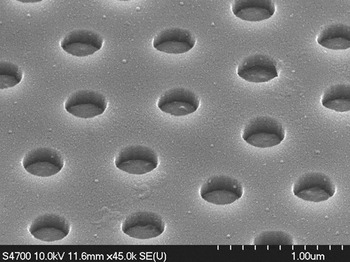
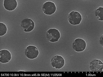
In recent years, some manufacturers have also relied on photonic crystal light structures patterned on the emitting face of LEDs to extract much larger amounts of light from the confines of the chips.Reference David, Benisty and Weisbuch32 These features, etched on the top surface of LED chips, are essentially cooperative in many-body diffractive structures that can be used to either inhibit or extract guided electromagnetic modes. Both one-dimensionalReference Hong, Kim, Kim, Lee, Song, Cho, Sone, Park and Seong33 and two-dimensional periodic structures have been investigated for this role.Reference Wierer, Steigerwald, Krames, O’Shea, Ludowise, Christenson, Shen, Lowery, Martin, Subramanya, Gotz, Gardner, Kern and Stockman34–Reference David, Fujii, Moran, Nakamura, DenBaars, Weisbuch and Benisty39 In practice, this requires etching shallow holes (∼300 nm deep and ∼300 nm in diameter) on the emitting facet of the LED.Reference Inoue and Ohtaka40 A scanning electron micrograph of one such structure etched in GaN is shown in Fig. 4.
Etched photonic crystal structure on the surface of a blue-emitting GaN LED.

Photonic crystals aid light extraction from LEDs through Bragg scattering and mode out-coupling from laterally propagating confined modes to vertically propagating in-air modes.Reference David, Fujii, Matioli, Sharma, Nakamura, DenBaars, Weisbuch and Benisty41 In this way, photonic crystals essentially steer light from a horizontal to vertical direction. This aspect of photonic crystal functionality can be tuned through a careful selection of various aspects of photonic crystal design. These include, among other parameters, the regularity class (symmetry) of the structure, hole diameter, hole pitch, hole depth, etch slant angle, and design wave length. Photonic crystal structures could be patterned on LED wafers using either direct-write electron beam lithography or one of several variants of nano imprint lithography.Reference Kang, Ann, Kim and Rahman42 The latter approach, due to its low fabrication cost, has been used for the mass manufacture of photonic crystal LEDs.
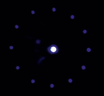
Photonic crystal LEDs can be either p-side up or flip-chip devices and can have light output between 1.5 and 2 times that from a similar but unpatterned device.Reference Rahman and De La Rue43 Shakya et al. have reported short wave length photonic crystal GaN LEDs emitting UV radiation at 333 nm.Reference Shakya, Kim, Lin and Jiang35 Jonathan Wierer and colleagues at Lumileds have demonstrated photonic crystal patterned GaN LEDs with nearly twice as much output flux as similar unpatterned LEDs.Reference Wierer, Krames, Epler, Gardner, Craford, Wendt, Simmons and Sigalas44 They showed that devices without photonic crystal had a near Lambertian radiation pattern while LEDs carrying an etched photonic crystal had heavily modified far-field radiation patterns. The non-Lambertian angular distribution of light from photonic crystal LEDs arises from the diffraction of light as it exits the LED chip through the photonic crystal structure. Figure 5 shows a 460 nm GaN LED chip optically excited by a 405 nm laser beam. Blue light is generated and as it comes out it creates a 12-dot pattern in the near-field due to the 12-fold symmetry photonic crystal pattern etched on the surface of the chip. Such devices are extremely important as solid-state replacements for existing mercury discharge tubes and in the future these will be used in applications ranging from lithography to water purification. Commercial photonic crystal LEDs have been available from several companies for specialized applications that can benefit from the narrow, collimated light output from these devices.
Laser light diffracting out of a photonic crystal-patterned LED chip. The 12-fold symmetry of the two-dimensional periodic structure is seen as a circular pattern of 12 secondary diffraction maxima.

Blue LEDs are also the device behind most white LEDs. While the white light can be obtained from a combination of red, green, and blue LEDs, this so-called RGB approach has been superseded by the much less expensive scheme of luminous conversion LEDs. These ‘LUCO’ LEDs consist of a blue or near UV LED coated with a yellow emitting phosphor, such as cerium-doped yttrium aluminum garnet (Ce:YAG). With an appropriate choice of cerium doping concentration and phosphor coating thickness, this luminescent material can convert a fraction of the blue LED's emission into yellow light. The combination of yellow and blue light then appears as a white emission to the human eye. It is even possible to tune the color temperature of these LEDs through adjusting the exact composition of the phosphor material. By doing this both cold and warm white LEDs could be fabricated. Phosphor-based white LEDs are described in more detail later in this article.
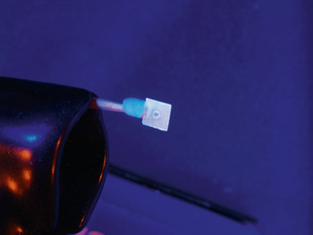
Furthermore, by combining LEDs of different color temperatures and by driving them with pulse width modulated current waveforms, stereochromic lights at variable color temperatures can be produced. Such luminaires have a cool and a warm white light LED in the same package. Having two LEDs of different chromaticities, such sources can generate various shades of white light by varying the relative amounts of light from each type of LED. Other than guest–host type phosphors, both quantum dotsReference Achermann, Petruska, Koleske, Crawford and Klimov45,Reference Mueller, Petruska, Achermann, Werder, Akhadov, Koleske, Hoffbauer and Klimov46 and crystal dislocationsReference Rahman and Johnson47 have also been used in generating white light with GaN LEDs. Figure 6 shows a specially modified GaN epilayer where dislocations are acting as an internal phosphor in generating white light under blue illumination. It is also possible to dope GaN with rare-earth elements, such as europium, to further broaden the range of colors that are possible from GaN LEDsReference Rahman48–Reference Steckl and Zavada51 but high-performance devices have not been reported from this material combination yet.
White luminescence from a blue/UV pumped dislocation-enhanced GaN epilayer.

Droop effect in GaN LEDs
MQW GaN/InGaN blue LEDs are now the fastest developing class of optoelectronic devices, being the mainstay of the fast-developing solid-state lighting industry. Many of their operational parameters such as light extraction efficiency and device resistance require further improvements. However, the largest single concern with them is due to their relative inefficiency when driven at high current levels. The decrease of electrical-to-optical energy conversion efficiency at high LED drive currents is a now well-known effect. This ‘droop’ effect has been widely debated in the recent literature.Reference Piprek52–Reference Wang, Wang, Wang, Hao, Luo, Dempewolf, Müller, Bertram and Christen54 While progress has been made,Reference Ni, Fan, Shimada, Özgür and Morkoç55,Reference Iveland, Martinelli, Peretti, Speck and Weisbuch56 an unequivocal explanation of its origin is yet to emerge. There is overall consensus, however, that droop will likely result in a fundamental limit to the operating efficiency of LED-based light sources. Despite much work devoted to understanding the origin of loss of LED efficiency at high drive currents, there is still considerable uncertainty about the exact or dominant cause of its origin. Among the likely candidates causing droop are effects such as Auger recombination (where an energetic electron shares its energy with another electron rather than undergoing radiative recombination), over-the-barrier leakage, and various polarization-induced effects. If indeed deleterious effects on LED performance that give rise to droop cannot be overcome, then LEDs will face a serious obstacle where their applications in high brightness sources are concerned. For instance, creating LED-based replacements for 100-Watt incandescent bulbs will be a monumental task if droop cannot be eliminated. Such pressing concerns are driving the quest to better understand the causes of droop in GaN LEDs. An interesting recent development related to this has been the development of laser-diode-powered white light sources. GaN/InGaN violet laser diodes emitting at 405 nm are now well-established devices. Their prices have come down sharply over the last few years and most importantly these devices do not exhibit droop. Thus GaN laser diodes could serve as an alternative pump source for phosphor-converted white light sources and this possibility is under investigation at this time.Reference Denault, Cantore, Nakamura, DenBaars and Seshadri57 Such laser-based light sources can offer other benefits that are not usually available from LED-based sources. These include a fuller white light spectrum that includes violet light and absence of perceptible shifts in color point because the phosphor is separate from the pump diode and is thus not subject to temperature variations.
Thermal management of LEDs
The reliability of LEDs is largely dependent on their thermal management i.e., how well the heat produced during device operation is removed.Reference Horng, Hong, Tsai, Wuu, Chen and Chen58,Reference Su, Yang, Hung, Lee and Chiang59 For ordinary GaN epilayer-on-sapphire LEDs, the heat produced in the epilayer can only escape through the sapphire substrate. However, the relatively low thermal conductivity of sapphire means that extracting heat in this way is very difficult. While such LEDs can be mounted on metallic heat sinks with thermal interface materials, the thermal bottleneck caused by sapphire remains. The low rate at which heat escapes from active LED layers manifests itself in high LED junction temperatures, which severely reduces the overall efficiency of LED operation and shortens their lifetimes. A more thermally conductive substrate would certainly help here and that is where SiC can help. GaN epilayers grown on SiC yield LEDs with much superior heat dissipation characteristics when compared to otherwise similar sapphire substrate devices. This is because of the much higher thermal conductivity of SiC (120–150 W/m K) as compared to that of synthetic sapphire (25–30 W/m K). SiC, however, is harder to grow and process into wafers, which makes SiC-based devices more expensive. Cree Corporation developed much of the GaN-on-SiC LED technology in the early years of this centuryReference Edmond, Abare, Bergman, Bharathan, Lee Bunker, Emerson, Haberern, Ibbetson, Leung, Russel and Slater60 and consequently holds most of the patents in this area. Cree remains the only company that produces SiC substrate GaN LEDs commercially. No matter which substrate is used, LED chips are bonded to heat conductive substrates for efficient heat removal during device operation. Although LEDs are much more efficient than incandescent lamps, they still generate a considerable amount of heat, especially when driven at high current levels. Unlike incandescent bulbs, this heat is unable to be radiated away and thus the chip has to be efficiently cooled or the LED will destroy itself through thermal runaway.Reference Chang, Das, Varde and Pecht61 Highly effective, thermally conductive, device packages have been developed with this goal in mind. The materials used to attach LED dies to package substrates play also a key role here. Bo-Hung Liou and colleagues at the National Chung Hsing University in Taichung, Taiwan have analyzed the effectiveness of various materials such as tin–silver–copper pastes with and without carbon nanotubes (CNTs) for this application and found that CNTs significantly enhance the thermal performance of die-attach materials.Reference Liou, Chen, Horng, Chiang and Wuu62 The relationship between different thermal resistances and observed failure modes has also been studied by this group who performed detailed scanning electron microscopy of a variety of failure modes at the LED die-attach pad interfaces.Reference Horng, Lin, Chiang, Chuang, Hu and Hsu63 The reliability of high power LEDs and multichip LED modules is crucially dependent on the thermal resistance between the LED chip (or chips) and the package substrate. A good model for the thermal circuit encountered in today's high power LEDs has been described by Jong Hwa Choi and Moo Whan Shin.Reference Hwa Choi and Whan Shin64 Their model indicated that the good thermal design can reduce the junction temperature of LEDs by up to 20%. It was mentioned previously that flip-chip LEDs exhibit much better thermal performance than usual LEDs with intact substrate. This is because heat is able to flow directly from its point of generation to the mount substrate. In a study of such devices on silicon and AlN substrates, Ming-Jer Jeng and collaborators at Chang Gung University in Korea found that flip-chip LEDs when properly bonded to high thermal conductivity substrates can show efficiency improvements of up to 7 times that of conventional LEDs.Reference Jeng, Chiang, Chang, Yen, Lin, Chang, Lai, Lee and Chang65 Heat from LEDs can also be removed through forced convection. While fan-cooled heat sinks have been around for a long time, new technologies based on vibrating diaphragm pumps have also been developed. These devices use vibrating piezoelectric membranes to force air through narrow orifices forming air jets that can efficiently cool hot components. A research collaboration between the University of Maryland and GE Global Research Center has described the performance characteristics of retrofit LED bulbs cooled by synthetic jets.Reference Song, Han, Bar-Cohen, Arik, Sharma and Weaver66 Their work provides an interesting comparison of degradation rate and lifetimes between passively and actively cooled LED luminaires.
GaN-on-Si LEDs
For the past ten years, much research effort has been devoted to growing thin monocrystalline GaN films on silicon wafers and making GaN LEDs out of such material. Over this period, much progress has been made in the epitaxial growth of GaN thin films on silicon substrates.Reference Mo, Fang, Pu, Liu and Jiang67–Reference Zhu, Wallis and Humphreys71 The principal logic behind this, otherwise disparate material combination, is to replace the usual sapphire substrate with cheap and widely available commercial grade silicon wafers. This scheme offers many other benefits besides.
Silicon has a substantially higher thermal conductivity compared to sapphire and thus LEDs made from GaN-on-silicon material are able to dissipate heat much faster than comparable LEDs made from conventional GaN-on-sapphire material. Moreover, unlike sapphire, silicon bonded to epitaxially grown GaN films can be removed easily through wet chemical etching techniques. This makes it possible to produce substrate-less flip chip LEDs at costs that are far lower and yields that are much higher than that when starting from sapphire substrate material. Again, this leads to LEDs capable of superior thermal performance which in practical terms means brighter devices. As if these were not enough, another attractive feature of this material combination lies in the fact that it enables processing on much larger substrates than has hitherto been possible. This is because sapphire substrates are usually available as 2-inch-diameter wafers (though material up to 4-inch-diameter can also be obtained, at significantly higher cost) but silicon wafers can be purchased economically in diameters of over 12 inches. This, coupled with the fact that much processing can be performed on existing and older silicon integrated circuit (IC) processing tools that can handle such larger wafers, means that processing costs can be drastically reduced. Each wafer can yield dozens of times more LED dies than was possible so far, boosting yields and dramatically cutting down the cost per die.
No matter how we look at it, this has been a major and very welcome development from the perspectives of both cost and energy utilization. Both the use of cheaper material and ease of fabrication directly lead to lower cost LEDs. This, in turn, can drive down the cost of LED light bulbs, making them much more attractive to consumers. Larger flip-chip LEDs made from GaN-on-silicon material will also make possible brighter light bulbs – another factor that has held back wide scale adoption of LED lighting technology. Proliferation of LED luminaires in both low and high wattage designs as well as their better performance on account of improved heat dissipation capability will reduce energy usage even further.
Clearly, GaN-on-silicon is a win–win technology but it has had to overcome many hurdles before its potential could be realized. Most of the problems were related to the mismatch between silicon as the growth substrate and GaN as the epitaxial film to be grown over it. While sapphire (aluminum oxide, Al2O3) has around 14% lattice mismatch with GaN, silicon has a somewhat larger 17% mismatch. This leads to growth stresses when even a thin GaN film is grown on top of silicon.Reference Ma, Zhu, Ming Wong, Zou and Lau72 The problem is further exacerbated by the fact that the thermal expansion coefficients of GaN and silicon are also very different. The difference in thermal expansion coefficient between GaN and Si, 5.59 and 3.59 × 10⁻⁶ K−1, respectively, at 300 K, leads to tensile stress in GaN and thus to crack formation upon cooling down from growth temperature.Reference Kukushkin, Osipov, Bessolov, Medvedev, Nevolin and Tcarik73 Despite these, special proprietary growth techniques utilizing carefully chosen epitaxial buffer material have made it possible to grow low stress GaN/InGaN layers on silicon substrates.Reference Hageman, Haffouz, Grzegorczk, Kirilyuk and Larsen74
At the time of this writing, GaN-on-silicon LEDs are being developed by several companies and some initial products are now commercially available. Notable among these are Lattice Power in China, Plessey Semiconductors in the U.K., Osram in Germany, and Bridgelux in the United States. It is expected that toward the end of 2015, LEDs made through this technology will begin large-scale replacement of sapphire-based LEDs, bringing the benefits of cost and performance to all.
Phosphors for white LEDs
All white LEDs have a blue-emitting LED at their core which excites a wave length converting material called a phosphor that is coated on top of the LED chip, as seen in Fig. 7. This LED + phosphor combination is universal for all contemporary commercial white LEDs. Due to the explosive growth of white LEDs, the majority of all blue LEDs produced annually are used for making phosphor-converted white LEDs.Reference Rahman75 Thus the market demand for blue LEDs is, for most part, being driven by the demand for white LEDs. However, blue LEDs, albeit essential, are only the pump sources for white LEDs. To produce white light, the blue emitters have to work with various kinds of phosphors. Broadly speaking, LED phosphors are luminescent materials that, when excited by blue light, generate broadband yellow light. The yellow light, in combination with the residual blue light from the pump LED, gives the impression of white light to the human eye.Reference Chen, Lin, Yeh and Liu76 Phosphors are thus central to the working of all white LEDs. In fact, the quality of white light produced is almost exclusively dependent on the properties of the phosphor used for making a white LED. Making better illumination-quality LEDs thus comes down to developing better phosphors, more than anything else. Thus phosphors appear as the driving force behind the increasing penetration of LEDs in all kinds of solid-state illumination applications.
Schematic diagram showing the structure of a packaged white LED.

LED phosphors usually comprise a host crystal, doped with a small quantity of one or more ‘activator’ ions. It is these activator ions that are responsible for the color conversion properties of phosphors, although the host matrix also plays a crucial role. The activator ions are usually (but not always) ions of one of the rare-earth atoms (also called lanthanides). Electronic transitions among the energy levels of the rare-earth ions are responsible for wave length conversion. The atomic structures of several rare-earth elements are such that they can efficiently absorb visible light photons at one wave length and convert them to photons at a longer wave length. Because longer wave length photons carry less energy than the shorter wave length ones so some energy is necessarily lost in this process. This is called the Stokes loss and accounts for most of the energy loss in a phosphor-driven light emitter. It is important to understand that most phosphors are two-component systems consisting of a host crystal matrix containing luminescent ionic centers. The role of the host matrix is extremely important in the wave length conversion process as it affects the energy levels of the dopant atoms and thus determines the absorption and emission wavelengths of the phosphor. The same ion doped in different crystal hosts will exhibit different light conversion characteristics. As an example, a typical phosphor used in many low-priced cool white LEDs is cerium-doped yttrium aluminum garnet (Ce:YAG). Here cerium ions are doped into a host crystal which is a mixed oxide of aluminum and yttrium. This was one of the first phosphors used for making white LEDs.Reference Yum, Seo, Lee and Sung77 Ce:YAG generates yellow light when excited with blue light such that the combined yellow and blue lights appear as a cool shade of white. To make warm white LEDs, broadband yellow phosphors can be combined with small amounts of red-emitting phosphors. It is also possible to manufacture LEDs with full spectrum white emission by compounding together three phosphors that separately emit in widely separated wave length bands.Reference Chen, Chu and Liu78 Such advances are enabling the new generation of high-performance LEDs with exceptional color rendering properties.
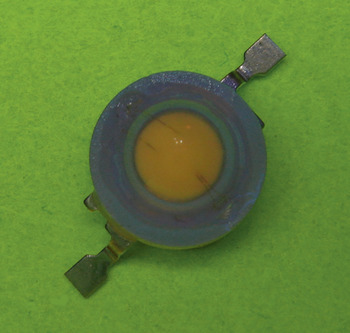
Phosphors are made by high-temperature solid-state reactions in specialized phosphor furnaces. Stoichiometric proportions of various inorganic compounds are finely ground, intimately mixed, and then heated to temperatures that may exceed 1000 °C. Phosphor furnaces can hold from 100 grams to several kilograms of material at a time. The high-temperature solid-state chemical reactions take place under an atmosphere of nitrogen or similar inert gas. Once the reaction has completed, the material is removed, reground, and may be washed in either water or organic solvents to remove any unreacted compounds. Mandatory testing is then performed after which the phosphor is ready for use with blue pump LEDs. Most LED manufacturers prepare a slurry of phosphors mixed with a thermoplastic resin. Polycarbonate and silicones are widely used for this purpose – the polymer acting as a binder to keep the phosphor in place. Figure 8 shows a white LED with its phosphor coating (yellow) and dome lens. The overmolded lens serves both to collect and collimate the light that is emitted from the LED + phosphor combinationReference Hsu, Wang, Ru Lin and Han79 and to protect the phosphor from the ambient atmosphere. While polymers are used in almost all commercial LEDs for this purpose, they do degrade slowly under heat stress and exposure to high optical flux.Reference Meneghini, Dal Lago, Trivellin, Mura, Vanzi, Meneghesso and Zanoni80 It is possible to use glass as an encapsulation material with better performance characteristicsReference Wang, Tsai, Liou, Cheng, Huang, Chang and Cheng81 but this usage is not widespread in the industry due to material and processing costs involved.
A 1 Watt-rated white power LED, showing the yellow phosphor, silicone encapsulation, and bond wires.

Phosphors based on rare-earth elements owe their popularity to the ease with which almost any color in the visible spectrum can be created by choosing appropriate combinations of host matrix and rare-earth ions. Not only can such phosphors be used for making all types of white LEDs but also used for making broadband color LEDs.Reference Rahman82,Reference Rahman83 Much of the current work in phosphor development for high color rendering index (CRI) and high efficacy light sources is directed toward developing phosphors with one, two, or even three rare-earth ions. Various emission properties of a phosphor can be tuned through a proper selection of the host matrix, rare-earth ion(s), and their doping concentrations. Matrix material selection is a critical factor here since the crystalline host has a profound effect on the active ion coordination chemistry. A proper choice of host crystal allows phosphor makers to engineer the crystal field around the doping sites of the ions. The electric field-induced crystal field splitting determines the energy level values of doped lanthanide ions. As an example of this kind of phosphor engineering, a magnesium aluminum silicate, Mg2Al4Si5O18 (MASO), crystal matrix doped with Eu2+, Ce3+, Tb3+, and Mn2+ ions was recently investigated as a new warm LED phosphor. It was shown that by altering the crystal structure and doping ions, CRI and color temperature could be successfully controlled.Reference Lu, Jia, Zhao, Lv and You84 The phosphor's luminescence profile was effectively changed by stimulating different energy migration pathways among active metal ions. However, the quantum efficiency of this phosphor needs to be improved further and thus work continues on gaining a better understanding of energy exchange in multi-rare-earth phosphors.
Phosphors based on rare-earths have sometimes sparked discussions on the economics and scarcity of rare-earths themselves.Reference Alonso, Sherman, Wallington, Everson, Field, Roth and Kirchain85 Apart from their use in phosphors, lanthanide elements have myriad other uses in such items as catalytic converters, powerful permanent magnets, batteries, various kinds of sensors, etc. Contrary to what their name would suggest, rare-earths are not truly rare and are in fact quite widely distributed in the earth's crust. However, due to their occurrence as secondary dilutions in the ores of other elements and the close chemical similarities between different lanthanides, these elements are not easy to mine. And while generally they are quite equitably distributed over the world's land mass, substantial concentrations that are amenable to economic mining are found in only a few locations. The specter of a possible supply crunch is, however, quite unfounded because there is sufficient current and projected future availability of rare-earth compounds to ensure an uninterrupted supply for many years to come. Most applications of rare-earths use only small amounts of these elements, in percentage terms. For instance, in LED phosphors, elements such as europium, terbium, or lanthanum are only used in minute amounts as optical dopants. For this reason, recycling of rare-earth compounds from LEDs is currently not economically advisable. From a long-term sustainability point-of-view, there do not appear to be any serious issues related to the availability of rare-earths, especially as there are good prospects for new sources such as deep sea mining to be developed in the coming years.Reference Kato, Fujinaga, Nakamura, Takaya, Kitamura, Ohta, Toda, Nakashima and Iwamori86
White lightReference Sun, Andrew Wang, Song Li, Wang, Zhu, Xu, Yang and Li87 and single colorReference Zhao, Bardecke, Munro, Liu, Niu, Ding, Luo, Chen, Jen and Ginger88 LEDs have also been made by using quantum dot materials as the wave length conversion medium. The II–VI quantum dots made from cadmium and zinc sulfides and selenides can be efficient luminescent materials for converting light from one color to another. Their absorption and emission spectra are dependent on their size so that proper size-controlled growth techniques can enable the production of quantum dots tuned to almost any desired color. Used singly, they can be used to make single color LEDs whereas a mixture of quantum dots can be used to construct a white LED with a tailored spectral profile. Usually six to eight quantum dots of different sizes have to be used for this purpose. Initially, there was some resistance to the use of quantum dots as luminophores in LEDs because of their propensity to oxidation over an extended period of time. This can result in short lifetimes and other reliability issues such as a gradual shift in color temperature with time. However, this has now largely been resolved with the use of core–shell quantum dots where quantum dots are encapsulated within a thin outer shell of a different but similar material. Core–shell quantum dots are much more robust than naked quantum dots and are now thus the material of choice for constructing quantum dot LEDs. The very small size of quantum dots (a few nanometers to a few tens of nanometers in diameter) enables them to be placed inside very small structures. Thus quantum dots can be placed inside the surface-etched depressions of a photonic crystal structure where they can get pumped by the radiation trapped inside the LED chip, as seen in Fig. 9. The low yield in the synthesis of size-selected quantum dots, however, means that their prices have remained high and thus this route for making white LEDs has remained largely an area of research curiosity alone.
Quantum dot material inside the shallow etched cavities of a photonic crystal structure.

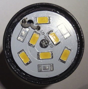
The current generation of phosphor-converted white LEDs is now produced globally in a verylarge scale. LEDs are used in their billions all over the world in all kinds of electronic and electrical appliances. This includes a rising usage in LED light bulbs. Sometimes called retrofit LED light bulbs, these devices contain a mains AC to low voltage DC switch mode power supply in addition to several LEDs. The inner view of a typical LED bulb is shown in Fig. 10 where six white surface mount device LEDs can be seen mounted on a metal core printed circuit board (MCPCB). This type of PCB helps to dissipate the heat that is generated by the LEDs. There may be additional heat sinking mechanisms built into the structure of the light bulb. A recent engineering study has described a LED luminaire design where LED chips are directly bonded to a vertical heat sink structure for improved heat dissipation.Reference Lin, Ying, Lin, Tai and Chen89
The inner surface of a LED bulb, showing surface mount chip LEDs on a MCPCB. The power supply is located underneath the PCB.

The lifetime of LED bulbs is usually specified as several tens of thousands of hours. This is the result of LEDs having exceptionally long lifetimes. The pump LEDs themselves can outlive all other components in a typical LED bulb. Their limitation mainly comes from the phosphor coating that is deposited on top of LED dies. At high-operating temperatures, deleterious reactions taking place in phosphors cause their light output to gradually diminish such that after twenty to thirty thousand hours the light intensity may fall to half that of new LEDs. As the degradation in phosphors is accentuated by temperature so keeping LEDs cool through better heat dissipation technologies goes a long way toward extending the life of LEDs and thus prolonging the useful life of LED bulbs. In some modern designs, the phosphor is physically separated from the blue pump LEDs, either by separating it from the LED by an air gapReference Chen, Chen, Lin, Wang, Yeh, Tsai, Shih and Kuo90 or by coating it on the inner surface of the bulb envelope, rather than placing it directly on LEDs. This so-called remote phosphor approach enables LED bulbs with lifetimes approaching fifty-thousand hours. Given the amazingly long life of LEDs, it is more probable that the bulb failure will be a result of a power converter component failing prematurely. Electrolytic capacitors are particularly failure prone and thus good LED bulbs make use of the best available capacitor technologies, such as solid electrolyte polymer film capacitors. In addition to a reduction in light output, the chromaticity coordinates of the light emitted by LEDs also change with aging. Thus, the color point of LED emission drifts slowly throughout its useful operating lifetime. Depending on the particular application, this may or may not be a problem. Han Kuei-Fu and colleagues have described their investigation of LED chromaticity shifts due to a number of factors in a recent study.Reference Fu, Lin, Chen, Chen, Cho and Sun91 They found that slight shifts in pump LED center wave length, aging-related yellowing of molding silicone, degradation of reflector, etc. are all factors that contribute to the shift of color point.
Societal impact of LED lighting
It would be rather simplistic to view LEDs as just a higher tech replacement for traditional light bulbs. This is because their cost, form factor (size and weight), and energy consumption are all so very different from that of incandescent lamps. These differences have led to a very different economic scenario for their usage.Reference Tsao, Saunders, Creighton, Coltrin and Simmons92 With LED lamps, gone are the days when light bulbs were just another domestic consumable – cheap to buy and frequent to replace. Buying LED-based luminaires now is much more like buying any other semipermanent electrical gadget, with costs amounting to many times that of incandescent bulbs together with lifetimes measuring many years of usage. People are still coming to terms with this shift in thinking when purchasing lighting for homes and offices. However, with continuing reduction in luminaire pricing and improvement in the quality of light, LEDs are now becoming increasingly accepted in all kinds of lighting applications. What is interesting to observe in this development is that LED lighting is changing the socio-economics of lighting at both luxury and sustainability levels.
The main argument in favor of LEDs is, of course, their significantly superior electricity-to-light conversion efficiency when compared to older electric lighting technologies. This has the potential to transform the way we generate, distribute, and use electric power, given that a large fraction of electricity generated by various means (renewable and nonrenewable) is used for illumination purposes. According to the U.S. Energy Information Administration, 12% of all electricity usage in the United States was for lighting in the year 2012. The figures for other developed industrialized countries are similar. As the transition from tungsten filament bulbs to LED luminaires is completed in the next decade or two, lighting will represent a much smaller share of electricity usage worldwide.
In addition to their use in built environments, LEDs are also migrating into other areas that were once the sole preserve of traditional light bulbs. This shift is natural because of their small size and power consumption. At the same time, they also provide other benefits that were not even conceivable until a few years ago. Perhaps, the best illustration of such usage is the recent introduction of LEDs for interior cabin lighting in passenger aircrafts. Boeing was the first to make use of LED lighting in its 787 ‘Dreamliner’ aircrafts. Lighting engineers designed the cabin lighting for this series of planes to satisfy both decorative sensibilities and circadian rhythms of air passengers.Reference Rahman93 The result not only looks esthetically pleasing but also serves the utilitarian purpose of keeping passengers from getting tired over long journeys. This is accomplished by adjusting the color and brightness of interior lighting to mimic normal light variation over the course of a day, as the travelers complete their journey (see Fig. 11). The result, with other refinements to the cabin environment such as slightly higher humidity and pressurization, is that people arrive at their destination fresher and less fatigued than was usual before the advent of such technologies.
The inner surface of a Boeing 787 Dreamliner aircraft, equipped with LED-based solid-state lighting.

By introducing LED lighting, together with other climate control technologies, Boeing has positively altered passenger expectations of air travel. This is obviously to Boeing's advantage but as it sets a precedent, other companies too are incorporating diode-based lighting into their offerings, making it an industry-wide standard.
Before aircraft interiors were equipped with LEDs, more down to earth vehicles such as cars were already experimenting with solid-state lighting. While cabin lighting is easy to install in road vehicles, manufacturers have been bolder in trying to replace the much brighter automobile exterior lights with LEDs. This trend has progressed so far that now even LED headlights have become available, at least on the more expensive models offered by a number of manufacturers.
In addition to their use for lighting in built-environments and vehicles, as described above, LEDs also provide lighting in all kinds of portable and mobile infotainment devices. From backlights in liquid crystal display TVsReference Jang, Jun, Jang, Lim, Kim and Kim94 and monitors to cell phones and projectors, LEDs are the engines that light up screens on all kinds of modern display devices. It is a fact that a substantial fraction (10–30%) of energy used by such devices is consumed by LEDs embedded in them. Thus future increases in LED efficiency will directly translate to a longer battery life for display-equipped gadgets as well as shaving off another 1–2% of grid energy usage.
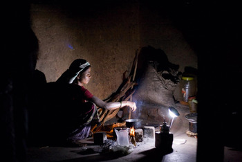
The social impact of LED lighting is even more visible in developing countries with large populations. Due to poor infrastructure maintenance and inadequate forward planning, many such countries face acute shortages of electric power that leads to frequent and prolonged power cuts. The recurring blackouts significantly affect patterns of normal activities after sunset and sets back progress in many ways. This is not merely an inconvenience as unplanned power outages also drive up crime figures and make it much harder to deliver a satisfactory standard of health care during the hours of darkness. Until a decade ago, there was little to do but resort to candles and oil lamps whenever the electricity failed. Fuel burning for light production increases air pollution and contributes to global warming. However, now there is a new alternative. Solar cell-powered LED lamps are now becoming popular in rural (and some not so rural) areas of developing countries in Asia and Africa (see Fig. 12).Reference Bond, Aye and Fuller95 Approximately 1.6 billion people do not have access to traditional electrical systems and, therefore, a significant number of people do not have access to safe, efficient, and inexpensive lighting technologies. Rebecca Hill and Kevin Curtin have examined the potential effects of distributing LED-powered lights to village residents in Cambodia.Reference Lee Hill and Curtin96 The use of solar-LED lighting for fishing has been studied by Evan Mills and colleagues.Reference Mills, Gengnagel and Wollburg97 They found that replacing fishermen's kerosene lanterns with LED lamps significantly cuts down on both energy usage and environmental pollution in countries such as Tanzania.
LED lanterns are getting popular in developing countries where there is shortage of reliable mains electric power.

In solar-LED illumination systems, solar cells charge rechargeable batteries during daytime, which power banks of LEDs after sundown. Cool, bright light from LED clusters, during power cuts, enables life to continue uninterrupted, allowing children to work on their homework and women to continue with their cooking activities.Reference Mukerjee98 The negative impact of erratic mains power supply is thereby considerably reduced. In an interesting article, Edwin Adkins and his colleagues have described off-grid energy services for the poor in Malawi, using solar power generation to charge batteries and provide lighting using LEDs.Reference Adkins, Eapen, Kaluwile, Nair and Modi99 Solar photovoltaic-based power systems running LEDs can also light up streets and one such system, developed in India, has been described by Sastry and colleagues.Reference Sastrya, Kamala Devi, Pant, Prasad, Kumar and Bandyopadhyay100 It is difficult to gauge the improvement to general health and well-being enabled by solar-LED lighting systems in developing countries. However, judging by the willingness of governments and agencies such as the World Bank to lend support to schemes for their installation,Reference Wong101 it becomes clear that solid-state power generation and lighting are having a huge impact on the lifestyle of the populace in many of the poorer countries of the world.Reference Pode102–Reference Jacobson105
ZnO as a potential future LED material
While GaN (and SiC) have been traditional semiconductors for making blue LEDs that serve as the engines for all white LEDs, a different semiconductor has been receiving sustained interest as yet another contender for this role. This semiconductor is ZnO – a wide band gap II–VI oxide semiconductor with a 3.3 eV wide direct band gap. The potential of ZnO as a blue LED material has been recognized for many years but there continue to be formidable challenges in making efficient and stable LEDs out of this transparent oxide. Whereas GaN also had to go through a phase of intense material and processing developments, the challenges with ZnO seem to be much more formidable. However, its many advantages compared to those offered by more established blue LED materials are such that work on ZnO keeps going in many academic and government labs around the world.
ZnO's higher exciton binding energy (60 meV) makes it a, potentially, better light emitter compared to GaN (26 meV). In simple terms, higher exciton binding energy reduces the likelihood of nonradiative recombination by encouraging bound electron–hole pairs (excitons) to form and then decay into a photon. In lower exciton binding energy materials, in contrast, fewer excitons get formed. While individual electrons and holes can still recombine and result in photon emission, as separate unbound entities, these charge carriers can more easily recombine nonradiatively at, for example, defect centers. This results in reduced photon emission and thus less bright light sources. The higher exciton binding energy of ZnO also makes possible related kinds of light sources such as polariton-based light emitters (incorrectly called polariton lasers or exciton lasers).
Another major advantage of ZnO over GaN – the current mainstream LED material – is its environmental sustainability. Whereas gallium, for making GaN, is an expensive and hard-to-get element, zinc is a cheap and abundant material. Furthermore, until recently, GaN was not available as a free-standing wafer and thus epitaxial films of GaN had to be prepared on ‘foreign’ substrates such as sapphire. Pure, monocrystalline wafers of ZnO are already widely available (see Fig. 13), making it possible to grow device-quality epitaxial layers on the native substrate. Currently, hydrothermally grown ZnO wafersReference Johann Nicholas, Franks and Ducker106,Reference Demianets, Kostomarov, Kuz’mina and Pushko107 are mostly available in small sizes but if their demand increases then they can also be produced in larger sizes and in much larger quantities. The availability of a free-standing bulk material not only makes ZnO epitaxial growth much easier to accomplish but also produces material of much higher quality with few threading dislocations and other growth-induced defects. The relative scarcity of defects together with the high exciton binding energy promise to produce LEDs with much higher performance metrics than the existing GaN-based devices. As a LED material, ZnO offers a number of other benefits.
Hydrothermally grown ZnO wafers. These n-type bulk wafers are 1 square centimeter in area and are 1 millimeter thick.

The refractive index of ZnO is 16% lower than that of GaN (2.15 versus 2.56, at 400 nm). This essentially means that light can be extracted more easily from the confines of a ZnO-based light emitting device. Photonic crystal light extraction structures on ZnO devices can be shallower and easier to fabricate than those on GaN devices. This should again lead to brighter devices that have a convincing external quantum efficiency advantage over GaN-based devices.
With ZnO, not only bulk wafer material is available but it is also easier to process it for making device structures. The chemical nature of ZnO is such that it can be easily etched through wet chemical processes.Reference Zheng, Du, Luo, Jia, Gu and Xue108–Reference Lee, Kim, Hyun, Tampo and Niki110 While dry etch chemistries are available for ultrasmall features, where needed (such as simple CH4-based chemistries),Reference Kim, Bae, Kim, Park, Seong and Adesida111–Reference Lim, Voss, Khanna, Gila, Norton, Pearton and Ren114 many devices could be fabricated by simpler wet etching processes. In many cases, even submicron features can be etched with acidic etchants, such as dilute orthophosphoric acid, containing appropriate surfactants. GaN, in contrast, is very difficult to etch through wet chemistries. A variety of ZnO nanostructures suitable for applications in sensing, electronics, and photonics have already been demonstrated.Reference Wang115 These nanostructures can be easily integrated with electrically active ZnO structures for making enhanced functionality devices.
Superior epitaxial optoelectronic material is possible with ZnO because a ZnO light emitter can be constructed entirely from the same material system with the substrate, buffer, charge transport layers, active layers, and current spreading layers all epitaxially grown in one MOCVD reactor with an integrated process flow. This both improves the material quality and reduces the growth cost and complexity.
ZnO can challenge the might of GaN if and when the technology for making good, stable p-type ZnO becomes available. Despite persistent efforts over many years, the device quality ZnO still remains elusive. The situation is interestingly reminiscent of the problem with GaN before it became a mainstream optoelectronic material. Just like ZnO, n-type GaN was easy to obtain but repeatable p-doping remained a tough challenge until it was finally demonstrated, thus opening the doors to all kinds of GaN-based devices – both electronic and optoelectronic. Doping, and especially p-type doping, is generally difficult with wide band gap semiconductors but ZnO presents its own challenges. The material is naturally n-type with the origin of its n-type conductivity not properly understood even after years of investigations. Even for doped p-type the hole concentration achieved is not as high as desired because of strong compensation from naturally occurring thermodynamic defects. More troublesome still, the p-type conductivity often falls off over time so that the material is electrically unstable and thus not suitable for making commercial devices. There have been many reports on p-type doping of ZnOReference Dai, Deng, Mao and Zang116–Reference Kaminska, Piotrowska, Kossut, Butkutė, Dobrowolski, Łukasiewicz, Barcz, Jakieła, Dynowska, Przeździecka, Aleszkiewicz, Wojnar and Kowalczyk118 but making robust p-type material is still a research goal.
Given the many and continuing problems with making p-type ZnO, there are relatively few reports in the literature on the fabrication of homojunction ZnO LEDs.Reference Zhao, Liang, Sun, Bian, Feng, Hu, Zhang, Liang, Luo and Du119–Reference Dong, Zhu, Zhang, Li and Du121 Instead, attempts have been made to fabricate ZnO LEDs using other more amenable structural schemes. The most widely used are various heterojunction LED structures where n-type ZnO is paired with various p-type semiconductors such as GaN,Reference Murai, Thompson, Masui, Fellows, Mishra, Nakamura and DenBaars122–Reference Bulashevich, Evstratov and Karpov124 AlGaN,Reference Alivov, Kalinina, Cherenkov, Look, Ataev, Omaev, Chukichev and Bagnall125 SiC,Reference Yuen, Yu, Lau, Rusli and Chen126,Reference Kim, Byun, Ie, Park, Choi, Choi and Angadi127 Si,Reference Ahn, Park, Mastro, Hite, Eddy and Kim128 or even conducting organic polymersReference Chang, Tsao, Pan, Chi, Wang, Chen, Ren, Norton, Pearton, Chen and Chen129,Reference Sun, Huang, Wang and Xu130 which usually show p-type conductivity. There are now many reports in the literature on such ZnO LEDs. Of these, the case of GaN grown on ZnO or vice-versa is especially interesting because the two materials have a rather small lattice mismatch of around 2.2%. Interestingly, the behavior of such devices is often different from how a simple homojunction ZnO LED is supposed to behave. Even ultraviolet-emitting ZnO LEDs have been attemptedReference Ryu, Lee, Lubguban, White, Kim, Park and Youn131 which may be a substitute for AlGaN UV LEDs in the future. While we are still far from the goal of a practical, low-cost, efficient ZnO LED, the progress that is being made is an indication of the importance that the worldwide scientific community attaches to the prospect of realizing this very attractive device.
Conclusions
Wide band gap semiconductors, from GaN to possibly ZnO in the future, are key materials for energy-efficient solid-state lighting. Their material and device technologies continue to develop rapidly with participation from laboratories right across the globe. In this field, laboratory research gets quickly translated into commercial products. As a result, LED efficacies have risen dramatically over the past years, from about 15 lumens/Watt in 2000 to around 200 lumens/Watt in the research labs in 2014. Concomitantly, the price of LEDs has dropped rapidly and with advancements in technologies such as GaN-on-Si LEDs and ZnO LEDs, the price will continue to fall for many years to come. There is little doubt that in another decade from now LED-based lighting will be more prevalent than other forms of electric lighting. Its energy efficiency, environmental sustainability, and operational convenience set it apart from all other lighting technologies that have been developed so far. It is little wonder then that government and world bodies are so interested in bringing about as rapid a transition to all-solid-state electric lighting as possible.
A number of companies are actively pursuing the development of high brightness LEDs for illumination applications. Prominent among them include Philips, Cree, Bridgelux, Osram, Sharp, Toshiba, Nichia, Citizen, Samsung, Seoul Semiconductor, and General Electric. Other smaller companies are also active in the development of LED-based lighting fixtures and illumination engines. Future developments will include large-scale commercialization of GaN-on-Si LEDs and the possible appearance of ZnO LEDs. Remarkably, much of this research and development on LEDs and solid-state lighting is increasingly based in the Far East. This fact is now driving energy-related policies in the West, aimed at bolstering such work through collaborative efforts between academic, government, and industrial labs. No matter where the developments originate, thanks to what is being at this time, we are assured of a literally brighter and cleaner environment through the proliferation of LED-based lighting in the years to come.