I. INTRODUCTION
Silicon nanowire (SiNW) arrays have important antireflective properties. Reference Peng, Wang and Lee1 One reason for this is their gradual variation of effective refractive index from air to substrate. Reference Convertino, Cuscuna and Martelli2,Reference Xie, Oh and Shen3 Another one is light trapping by multiple scattering events, Reference Convertino, Cuscuna and Martelli2,Reference Street, Wong and Paulson4 which increases the probability for light absorption. Reference Street, Wong and Paulson4 For these reasons their main application is for light enhanced absorption in Si photovoltaic solar cells. Reference Lin, Hua, Huang and Shen5,Reference Jiang, Qin, Li, Wang, Ma and Chang6 Another advantage for this application is the possibility of decoupling light absorption and charge carrier collection into orthogonal directions. This condition is satisfied with a junction in the radial direction, and the nanowire (NW) axis parallel to the incident light direction, Reference Spurgeon, Atwater and Lewis7,Reference Kayes, Atwater and Lewis8 for example, normal incidence of light when NWs are perpendicular to the substrate plane. In this way, the solar cell requirements on the minority carrier diffusion length of the absorber material are reduced significantly in comparison to planar geometry. Reference Spurgeon, Atwater and Lewis7–Reference Baxter and Aydil10
Silicon nanowires (SiNWs) were first obtained in 1964 by Wagner and Ellis by a vapor–liquid–solid mechanism. Reference Wagner and Ellis11 Since this very first synthesis, many methods have been developed for the growth of SiNWs, such as pulsed laser deposition, Reference Morales and Lieber12,Reference Zhang, Tang, Wang, Yu, Lee, Bello and Lee13 gas-phase molecular beam epitaxy, Reference Schubert, Werner, Zakharov, Gerth, Kolb, Long, Gösele and Tan14 electron beam lithography, Reference Juhasz, Kylmänen, Galeckas and Linnros15 and chemical vapor deposition. Reference Stelzner, Pietsch, Andrä, Falk, Ose and Christiansen16,Reference Lu, Li, Kong, Guo and Li17 Among the many methods developed, self-assembly electroless metal deposition (SAEMD) nanoelectrochemistry in an ionic silver HF solution through selective etching is a simple way to prepare SiNW arrays. Reference Peng, Yan, Gao and Zhu18–Reference Dalchiele, Martín, Leinen, Marotti and Ramos-Barrado21 This method has several advantages with respect to other SiNW preparation techniques. First, since the as-prepared SiNWs are an integral part of the Si wafer substrate, they provide a direct 1D and uninterrupted pathway for charge transport to the substrate, i.e., SiNWs have a direct, high quality electrical contact with the underlying silicon substrate, and are robust and do not peel off from the substrate. In addition, the electrical properties of SiNWs are directly inherited from the bulk Si substrate, thus there is no need of further doping for conductivity control. In this item an important fact is that the orientation of NWs depends on crystalline orientation of bulk crystalline Si (c-Si) substrate. Reference Wu, Zhang, Zheng and Cheng22 Finally, due to the surface roughness of the SiNWs, they are almost nonreflective. Reference Branz, Yost, Ward, Jones, To and Stradins23,Reference Oh, Yuan and Branz24
In the past, several works regarding optical properties of SiNWs were published. Sturmberg et al. Reference Sturmberg, Dossou, Botten, Asatryan, Paulton, de Sterke and McPhedran25 described the optical properties of the SiNWs using a semianalytical modal method. The electromagnetic waves inside the array are described by a superposition of Bloch modes. Studying the properties of each Bloch mode separately, mainly their reflection and propagation, it can be concluded that absorption is dominated by a few modes. These modes are characterized by huge absorption caused by a good coupling with the incident electromagnetic field, a large concentration of energy inside the SiNWs and strong Fabry Perot resonances. Knowing that absorption process of SiNWs depends on a few Bloch modes, it can be manipulated by changing the geometry of the array. These numerical studies were made considering SiNW ordered arrays with a defined lattice period and NW diameter. Finite difference time domain (FDTD), finite element method, and transmitted matrix method were used. However, SiNW samples prepared experimentally have a certain degree of disorder. Bao and Ruan Reference Bao and Ruan26 studied SiNW arrays, using also FDTD simulations, including a diameter distribution of the NWs. Different diameters have different resonance wave lengths of absorption. Therefore, if there is a distribution of diameters, the absorption band is wider. This study also concluded that a disorder of the NW positions (not periodic) causes an absorption increment. Lagos et al. Reference Lagos, Sigalas and Niarchos27 obtained the same results using another method called rigorous coupled wave approach (RCWA). Also they studied the orientation disorder. When the orientation disorder increases, the absorption decreases. Xie et al. Reference Xie, Oh and Shen3 used a model of array for RCWA simulation. The model considers an ideally periodic SiNW array, including NW aggregation and its tapering nature. For RCWA simulation, the top radius of the NW is smaller than its bottom radius. Moreover, they considered three tapered regions consisting in 10% top, 80% middle, and 10% bottom. The periodicity, the top radius, and the bottom radius were obtained by scanning electron microscopy (SEM) studies. The experimental and theoretical results obtained by Xie et al. Reference Xie, Oh and Shen3 demonstrated that SiNW arrays exhibit an antireflection behavior independent of angle and light polarization. But in their experiments, Xie et al. Reference Xie, Oh and Shen3 used light with a defined wave length (514.5 nm). Yamaguchi et al. Reference Yamaguchi, Shimizu, Morosawa, Takase, Chen, Lu, Chien and Shingubara28 studied the dependence of reflectance with the degree of aggregation of NWs at their top ends. A parameter NN = A/B indicates the average number of NWs in a bunched structure. A is the density of NWs and B is the density of bunched structures. This parameter is used to evaluate the aggregation degree of NWs. The maximum NN studied by Yamaguchi et al. Reference Yamaguchi, Shimizu, Morosawa, Takase, Chen, Lu, Chien and Shingubara28 was 2180. This work concluded that when the degree of aggregation increases (NN increases), the reflectance at wave length above 500 nm decreases, according to microscale pyramidal structure. Reference Li, Wang, Zhao, Zhou and Diao29,Reference Sun and Tang30 The light incident on the rough surface is reflected several times among the surface of neighboring pyramidal structures. Also there is a mixture of microstructure and nanostructure which enhances the absorption in a wide visible wave length band. In this study, this very small optical reflectance and its relation with c-Si orientation are studied for SiNWs grown from both (111) and (100) Si wafers. Moreover, the influence of light polarization with substrate orientation is also investigated.
II. EXPERIMENTAL
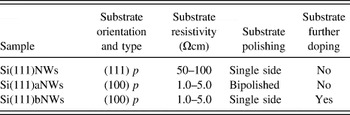
Si(111) wafer chips, 500 μm thick, p-doped (50–100 Ωcm) and Si(100) WCh, 280 μm thick, p-doped (1.0–5.0 Ωcm), with areas of ∼1 cm2 were used to synthesize SiNWs. Si(111) wafer chips were single polished, whereas Si(100) wafer chips were both side polished (a) and single polished (b), as it is shown in Table I. Additionally, Si(100)b wafer chips were n doped by using a spray coating technique. For this, a homemade solution has been used as a liquid precursor. The composition of the solution was 4% H3PO4 + 0.1% Triton X-100 + 12% 2-butanol + 18% ethanol + 65.9% DI H2O(w/w). The films were deposited in a self-made spray coating apparatus at room temperature (RT) with a pressure of 2.5 bar and a nozzle to substrate distance of 10 cm. The liquid precursor flow was controlled by an automated perfusion pump. The deposition and diffusion condition resulted in sprayed volume of 5 μL/cm2. Drying is a critical step. It determines layer thickness and hardness. It has been carried out at 150 °C for 1 min. Diffusion was performed in a quartz tubular atmospheric furnace at 900 °C for 60 min. The following steps of the synthesis were the same for all wafer chips. They were first washed in boiling acetone for 10 min and subsequently in isopropanol at room temperature, with sonication for 5 min. They were oxidized in H2O2/HCl/H2O (2:1:8) at 80 °C for 15 min to remove any trace of heavy metals and organic species, rinsed thoroughly with deionized water, etched with 10% aqueous HF for 10 min, rinsed with water again, dried under a stream of N2 and immediately used as a substrate in the SiNW growth process. The SiNWs have been synthesized by SAEMD nanoelectrochemistry on the Si WCh in an ionic silver HF solution (sol) through selective etching. Reference Dalchiele, Martín, Leinen, Marotti and Ramos-Barrado20,Reference Dalchiele, Martín, Leinen, Marotti and Ramos-Barrado21 The cleaned Si WCh were immersed into an aqueous HF/AgNO3 sol for 15–30 min at RT (the concentration of HF and AgNO3 here are chosen to be 5.0 and 0.04 M, respectively). The length of SiNWs could be effectively controlled through tuning the treatment time; in the present case, one hour treatment has been applied. After the treatment, the as-synthesized samples were rinsed thoroughly in deionized water and dried at RT. Then, the SiNWs were dipped in 30 wt% HNO3 aqueous sol for 60 s and repeated for several times to remove all residual Ag from the SiNW surfaces. After the HNO3 bath, no Ag peaks appeared in the energy dispersive x-ray spectroscopy (results not shown). SEM pictures were obtained using a JEOL JSM-5410 apparatus (Tokyo, Japan).
Description of samples.

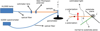
Total reflectance R t (diffuse + specular) and total diffuse reflectance R dt were measured by an integrating sphere Ocean Optics (OO) ISP-REF and an OO S2000 spectrometer (Winter Park, FL). A lambertian surface of spectralon OO WS-1 SL White Reflectance Standard was used as reference. Because specular reflectance of SiNWs is very low, diffuse reflectance R d was measured by varying the angle of incidence θ. The experimental setup is shown in Fig. 1. The incident light from an OO HL2000 halogen lamp was collimated by an OO 74Vis Collimating Lens. R d was detected by an optic fiber with 100 μm diameter coupled with the OO S2000 (acting as its entrance slit). The other end of the fiber was arranged close to the sample, which is mounted on a goniometer. It allows varying the angle of incidence θ, in a quasi-Littrow configuration. The axis of rotation and the plane of the substrate are parallel to the vertical direction k (see Fig. 1), which is perpendicular to the plane of incidence. A Glan Thompson polarizer was arranged after the collimating lens. The two distinct polarizations (see schematics to the right of Fig. 1) were p (light electric field parallel to the plane of incidence) and s (perpendicular to the plane of incidence).
Experimental setup for R d measurement with polarized light. Schematic to the right describes the p and s light polarizations and the angle of incidence θ.

III. RESULTS AND DISCUSSION
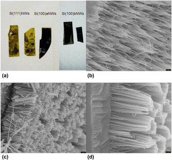
Figure 2 shows the images of SiNWs prepared on Si(111), Si(100)a, and Si(100)b c-Si substrates, which is to be called Si(111)NWs, Si(100)aNWs, and Si(100)bNWs, respectively. The Si(111)NWs have a brown–yellow appearance to the naked eye, with a milky shimmering like brightness when looked sidewise. Meanwhile, the Si(100)aNWs and Si(100)bNWs are dull black [Fig. 2(a)]. The SEM images [Figs. 2(b)–2(d)], with a tilting angle of 60°, show that the NWs have large aspect ratio (130–200 nm diameters, with 5–20 μm length). In both cases, there is aggregation of NWs at their top ends. Reference Convertino, Cuscuna and Martelli2,Reference Lin, Hua, Huang and Shen5 But while the Si(111)NWs have a disordered slanting morphology [Fig. 2(b)], Si(100)aNWs and Si(100)bNWs have an ordered one, with NWs normal to the substrate [Fig. 2(c)]. This agrees with the fact that in both cases the NWs grow along <100> directions. Reference Wu, Zhang, Zheng and Cheng22
(a) Image of Si(111)NWs (left), Si(100)aNWs (center), and Si(100)bNWs (right). SEM image with a tilting angle of 60° of (b) Si(111)NWs, (c) Si(100)aNWs, (d) Si(100)bNWs. The black bar in (b), (c), and (d) at right-side bottom is 2 μm.

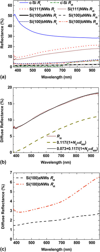
Figure 3(a) shows R t and R dt of SiNWs and c-Si. R t of polished c-Si decreases with wave length and shows a peak (∼380 nm) which corresponds to Γ25′-Γ15 direct transition. Reference Nelkomsky and Braunstein31 Meanwhile, R dt of c-Si shows a step (between 700 and 800 nm) which corresponds to Γ25′-L1C indirect transition. Reference Forman, Thurber and Aspnes32 The spectral shapes change drastically for SiNWs. R t of SiNW samples are smaller than R t of polished c-Si. The peak corresponding to Γ25'-Γ15 disappears for all samples. The step corresponding to Γ25'-L1C disappears for Si(111)NWs [see also Fig. 3(b) for R dt]. However, Si(100)NWs R dt spectra still show this step, although it is less abrupt than the step of Si-c R dt spectra [see Fig. 3(c)]. For Si(111)NWs, the smooth monotonic increase of R dt with wave length gives them their brown–yellow appearance. Although both R dt and R t have similar spectral shape, the first one is smaller than the second one because the specular reflectance is still important in this case. For Si(100)bNWs, R dt is also smaller than R t, however for Si(100)aNWs R dt and R t are almost equal (vanishing specular reflectance). Moreover, for both samples prepared from Si(100) wafer chips, they are much smaller than for Si(111)NWs, in agreement with their dull black appearance. It can be explained by the ordered nature of the NWs [see Figs. 2(c) and 2(d)] which causes a gradual change of the effective refractive index from the air to the substrate. Reference Convertino, Cuscuna and Martelli2,Reference Xie, Oh and Shen3 This effect improves the light absorption diminishing the reflectance of the samples. As the light interacts more strongly with the samples their spectra include the absorption edge present in the polished c-Si diffuse reflectance [see Figs. 3(a) and 3(c)].
(a) R t and R dt for polished c-Si and SiNWs. For Si(100)aNWs, both R t and R dt curves are indistinguishable. (b) Measured R dt for Si(111)NWs and modeled R dt by an ensemble of diffuse reflectors. (c) Measured R dt for Si(100)aNWs and Si(100)bNWs with enlarged vertical scale.

The changes in Si(111)NWs R dt can be modeled as an ensemble of diffuse reflectors. Reference Xie, Oh and Shen3 In this model, the mat of Si NWs is on a partial reflective surface. An exponential distribution is used to obtain the reflectivity of the mat without considering the substrate. This distribution, P(N), gives the probability that a photon is reflected out of the mat after N scattering events:
 $$P\left( N \right) = N_0^{ - 1}\exp \left( {{{ - N} \mathord{\left/ {\vphantom {{ - N} {{N_0}}}} \right. \kern-\nulldelimiterspace} {{N_0}}}} \right)\quad .$$
N 0 is the average number of scattering events in the mat before reflection. Reference Street, Wong and Paulson4 It is assumed to be independent of the scattering cross section of a particular mat. In each scattering event, the fraction of photons which are not absorbed is exp(−αd NW) where α is the absorption coefficient of Si (obtained from tabulated data Reference Green and Keevers33 ) and d NW is an absorption length, expected to be roughly the NW diameter (assuming that all NWs are lying on their side). Reference Street, Wong and Paulson4 According to this model, the R dt of a mat (R dtMat) of diffusing NWs, neglecting transmittance, is:
 $${R_{{\rm{dtMat}}}} = \int_0^\infty {P\left( N \right)\exp \left( { - \alpha N{d_{{\rm{NW}}}}} \right)} dN = {\left[ {1 + {N_0}\alpha {d_{{\rm{NW}}}}} \right]^{ - 1}}\quad .$$
N is big enough to be considered as a continuous variable. The optical properties of the substrate have to be considered when transmission is significant through the mat. A fraction T of the incident light is transmitted through the layer. Another fraction of the transmitted light is reflected in the substrate. To study transmission through the mat, a model for the light scattering is necessary. This model depends on Rayleigh-Mie theory.
Reference Silverman34
NW size, light wave length, and density of the mat are its relevant parameters. If scattering is big enough to obtain negligible transmittance, R is approximately
 ${R_{{\rm{dtMat}}}}\left( {R \approx {R_{{\rm{dtMat}}}}} \right)$
.
Using Eq. (1), N 0 d NW = 3 × 10⁻⁴ cm corresponding to 130–150 nm NW diameter, Reference Convertino, Cuscuna and Martelli2 R dtMat almost vanishes into the UV, and it is 0.97 at 950 nm (where αN 0 d NW = 0.03). The following corrections are then needed to adjust the measured R dt:
 $${R_{{\rm{dt\ }}}}\∼\,\,{R_{{\rm{NS}}}} + \left( {{R_{{\rm{dt@}}950\,{\rm{nm}}}} - {R_{{\rm{NS}}}}} \right){{{R_{{\rm{dtMat}}}}} \mathord{\left/ {\vphantom {{{R_{{\rm{dtMat}}}}} {{R_{{\rm{dtMat@}}950\,{\rm{nm}}}}}}} \right. \kern-\nulldelimiterspace} {{R_{{\rm{dtMat@}}950\,{\rm{nm}}}}}}\quad ,$$
where R NS is an additive correction, Reference Street, Wong and Paulson4 whose value can be obtained from the value of R dt at 380 nm (R dt@380nm = 0.073). (R dt@950nm − R NS)/R dtMat@950nm is a factor of R dtMat which allows adjusting the IR value (R dt@950nm = 0.18). Equation (3) which corresponds with full line in Fig. 3b fits very well the Rdt data (dotted curve) of Si(111)NWs'.
The absorption edge corresponding to Γ25'-L1C that appears for the more ordered Si(100)aNWs and Si(100)bNWs R dt [see Fig. 3(c)] is not present in the spectra deduced from Eq. (2). Therefore, the corresponding model is not as suitable for Si(100)NWs as in the disordered Si(111)NWs.
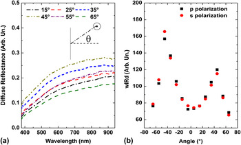
Figure 4(a) shows R d of Si(111)NWs, for s-polarized light and for different θ values. To study the θ dependence, the wave length integrated diffuse reflectance (wIRd) between 380 and 900 nm was calculated. The results are shown in Fig. 4(b). There is a relative maximum between 40° and 50° for Si(111)NWs. These results can be interpreted considering that NWs grow along <100> directions. Therefore, there are some NWs whose axis is parallel to [100] direction, other ones whose axis is parallel to [010] direction and some other ones whose axis is parallel to [001] direction. Reference Wu, Zhang, Zheng and Cheng22 Indeed, for Si(111)NWs, the sample was oriented such that the [001] direction lies in the plane defined by the k vector shown in Fig. 1 and the normal to substrate surface (orientation obtained from x-ray diffraction pole figure, results not shown). For θ ∼ ±39.2°, light approaches normally to [100] or [010] directions (i.e., normally to some of the NW axis) corresponding to the maximal NWs geometrical cross section, i.e., maximum backscatter reflectance. This θ is close to the maxima shown in Fig. 5(a) within the experimental θ step, and is responsible of the shimmering like brightness of these samples. So this effect is due to NW orientation. The difference in maximum intensities (for θ > 0 or < 0) is due to the random growth of NWs in any of the <100> directions. Reference Wu, Zhang, Zheng and Cheng22 There is no clear difference between wIRd for p-polarization and wIRd for s-polarization with respect to θ.
(a) R d for s-polarization of Si(111)NWs varying θ (schematics show polarization). (b) wIRd, area below R d of Fig. 4(a).

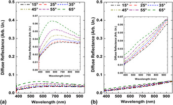
R d for s-polarization of (a) Si(100)aNWs and (b) Si(100)bNWs varying θ (inset is zoomed vertical axis).

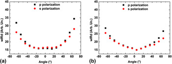
R d of Si(100)aNWs and Si(100)bNWs, for s-polarized light and for different θ values, is shown in Fig. 5, while Fig. 6 shows the wIRd against θ. wIRd increases monotonically with θ for both cases. The results can be interpreted considering that NWs grow along [100]. With growing θ, the angle between NW axis and light direction increases. Also, the wIRd increment for p-polarization is greater than the one for s-polarization. This is coherent with a polarization dependent effective refractive index n Reference Oton, Gaburro, Ghulinyan, Pancheri, Bettotti, Dal Negro and Pavesi35 :
 $${n_{\rm{p}}}\left( \theta \right) = {\left( {n_{\rm{s}}^2 + \left( {{n_{\rm{p}}}{{\left( {{{90}^^\circ }} \right)}^2} - n_{\rm{s}}^2} \right){{\sin }^2}\theta } \right)^{1/2}}\quad ,$$
where n p(θ) is the effective refractive index for p-polarization, and n s, which does not depend on the angle of incidence, is the effective refractive index for s-polarization. According to this equation, n p depends on the angle of incidence θ. If n p(90°) > n s, then n p(θ) > n s for all θ. As the reflected light intensity increases for larger changes of n between air and that of the SiNW layer, p-polarization reflectance should be greater than the one for s-polarization. Equation (4) can be interpreted qualitatively as follows. Reference Gómez Rivas, Muskens, Borgström, Diedenhofen, Bakkers and Wang36 For s-polarization, the electric field is always perpendicular to the NW axis (Fig. 1), if they grow normal to the substrate surface [Fig. 2(c)] ([100] direction). So the effective index of refraction for s-polarization n s is independent of the angle of incidence. Meanwhile, for p-polarization, which is parallel to the plane of incidence as the NW axes, the electric field has a parallel component along these axes (see Fig. 1). Although they are perpendicular for normal incidence (θ = 0, as for the s-polarization) this parallel component increases with θ. As the SiNWs effective n p is higher along this direction, the wIRd at large θ must be higher for p than for s-polarization: n p(0°) = n s, n p(90°) > n s. Note that the difference in wIRd between both the polarizations shown in Fig. 6 (at least for larger θ) is clearly larger than their difference in the whole span shown in Fig. 4(b). This can be understood because of the more disordered nature of Si(111)NWs [see Fig. 2(b)]. This disorder is responsible for the strong light scattering in the NWs that allows writing Eq. (2) that governs the spectral shape of Si(111)NWs R dt.
wIRd, area below R d of Fig. 5: (a) Si(100)aNWs and (b) Si(100)bNWs against θ.

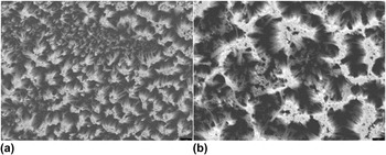
Finally, the inset of Fig. 5(a) shows that (especially for higher θ), the R d for Si(100)aNWs has a bump structure at about 550 nm which also appears in Si(100)bNWs [Fig. 5(b)], but it is weaker. For Si(111)NWs, it is imperceptible. Street et al. Reference Street, Wong and Paulson4 observed a similar feature in R dt spectra. The decrease in shorter wave length and larger wave length is explained by zero transmission and zero absorption behaviors. But in this work the bump is not present at R dt spectra, it only appears at R d spectra. As it has a blue shift when the angle increases it may be due to interference effect as suggested by other authors. Reference Convertino, Cuscuna and Martelli2,Reference Xie, Oh and Shen3 Actually, interference effect may depend on incidence angle, but such dependence should not appear so strongly due to zero transmission and zero absorption behaviors. Therefore, this structure might be due to interference effects, Reference Convertino, Cuscuna and Martelli2,Reference Xie, Oh and Shen3 which appear more clearly when the array is more ordered as in Si(100)aNWs [see Fig. 2(b)]. In effect, Figs. 7(a) and 7(b) show that for Si(100)bNWs the number of NWs involved in one agglomeration at their top ends is bigger than for Si(100)aNWs. Thus, NWs in Si(100)aNWs are less curved at their top end and they are more vertical. The aggregations for Si(100)bNWs are much stronger than for Si(100)aNWs. Therefore, the presence and the clarity of this spectral structure reflect the ordered nature of these SiNW arrays. This behavior and the dependence upon light polarization allow considering Si(100)NWs as a layer with an effective refractive index. In sample Si(111)NWs, in spite of the existence of agglomerations, the nanostructures predominate and their reflectance can be modeled by an ensemble of diffuse reflectors. As Si(111)NWs is the sample with the most disordered array of NWs, the interference effect is almost absent in them.
SEM image of (a) Si(100)aNWs and (b) Si(100)bNWs. Black bar in (a) and (b) at right-side bottom is 2 μm.

IV. CONCLUSIONS
The optical properties of SiNWs prepared onto Si(111) and Si(100) crystalline substrates (c-Si) by electroless metal deposition were studied. Those prepared onto Si(111) (Si(111)NWs) have a brown–yellow appearance while those prepared onto Si(100) (Si(100)NWs) have a dull black appearance to the naked eye. The total reflectance (R t) and total diffuse reflectance (R dt) of SiNW spectral shapes change drastically in relation to c-Si. SiNWs have a smaller R t than polished c-Si. R dt for Si(111)NWs can be modeled as an ensemble of diffuse reflectors. Besides, diffuse reflectance R d for Si(111)NWs does not depend strongly on light polarization, but the wIRd shows maxima at certain angles of incidence θ. They can be explained if NWs grow along <100> directions. For Si(100)NWs, wIRd increases monotonically with θ, wIRd for p-polarized incident light being greater than that for s-polarized light. Also, R d spectra show structures that correspond to interference effects. Thus, Si(100)NWs can be considered as a thin film whose refractive index depends on the light polarization.
ACKNOWLEDGMENTS
Comisión Sectorial de Investigación Científica (CSIC) of the Universidad de la República; Agencia Nacional de Investigación e Innovación (ANII); PEDECIBA – Física, in Uruguay. Junta de Andalucía, Project P07-FQM-02573 in Spain.