I. INTRODUCTION
CuInSe2-based solar cells have attracted a great deal of interest for both scientific fundamental research and scale-up production due to both the high performance and possibility of a low-cost production.Reference Sakurai, Islam, Uehigashi, Ishizuka, Yamada, Matsubara, Niki and Akimoto1–Reference Niki, Contreras, Repins, Powalla, Kushiya, Ishizuka and Matsubara3 Various processing techniques, which include coevaporation,Reference Niki, Contreras, Repins, Powalla, Kushiya, Ishizuka and Matsubara3, Reference Schöldström, Zimmermann and Edoff4 sputtering,Reference Shi, Li, Zhang, Liu, Sun and Huang5, Reference Kaelin, Rudmann and Tiwari6 and electrodeposition,Reference Bhattacharya, Batchelor, Ramanathan, Contreras and Moriarty7, Reference Fernandez and Bhattacharya8 have been used for preparation of the high quality Cu(In,Ga)Se2 (CIGSe) thin films. The record-breaking efficiency of 20.3% has already been achieved for small area cells (<0.5 cm2) by coevaporation.Reference Jackson, Hariskos and Lotter9 However, multisource evaporation, which has drawbacks such as the complexity in process, high production costs, and difficulties in scaling up, has been seen to date as a laboratory-scale production technique.Reference Dhere10 In terms of large-scale applications, one of the promising approach is two-stage processing of thin chalcopyrite films, involving deposition of Cu–In–Ga precursors with industrial growth processes in the first step followed by their selenization using H2Se gas or Se vapor.Reference Gremenok, Zaretskaya, Zalesski, Bente, Schmitz, Martin and Moller11 Se (vapor) does not require the sophisticated equipment usually required for the extremely hazardous H2Se gas and the unused excess Se can be easily recycled.Reference Lakshmikumar and Rastogi12
In the first step of CIGSe absorber preparation, the sputtering parameters have a direct effect on phase composition and surface roughness of alloy precursor, which may influence the properties of CIGSe absorber. Especially, phase composition of alloy film produced by sputtering is at metastable state, which does not agree with the equilibrium diagram. In the temperature rise period of selenization process, phase transformation and surface morphology change may take place before metallic precursor reacted with Se. In this paper, a lot of pinholes were found in CIGSe films produced by selenizing the Cu–In–Ga alloy precursor, which was sputtering deposited at ambient temperature. Sputtering substrate temperature of 150 and 250 °C was then applied. The phase composition and morphology of Cu–In–Ga precursor thin films as function of sputtering substrate temperature were investigated. Smooth, compact, and single chalcopyrite phase CIGSe thin films were finally obtained. The presence of pinholes, which existed in the films before, was avoided.
II. EXPERIMENTAL
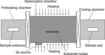
Two specially designed alloy targets were prepared intentionally. One was CuIn alloy target with copper to indium ratio [Cu]/[In] = 0.92 to obtain poor-Cu absorbers in following selenization processes and another was CuGa alloy target with copper to gallium ratio [Cu]/[Ga] = 1. By adjusting the sputtering time and current of the two targets, Cu–In–Ga metallic precursors with Ga/(In + Ga) atomic ratio of 0.3 and thickness of almost 1000 nm were prepared by magnetron sputtering two targets simultaneously. Three substrate temperatures (ambient temperature, 150 °C, and 250 °C) were applied during metal precursor deposition. All samples were deposited on soda lime glasses, which were ultrasonically cleaned sequentially in NaOH solution, HNO3 solution, and deionized water, and then were blow-dried in nitrogen. Then, the metallic precursors were placed in a three-chamber furnace (see Fig. 1), which can be easily scaled up to provide a large area in-line sequential CIGSe process. Metal precursors were first put into preheating chamber and then were pushed into the selenization chamber through load lock after the selenization chamber reached the set temperature. The preheating temperature and the selenization temperature were set at 250 and 550 °C, respectively. After 15 min of selenizaiton time, the samples were transferred to cooling chamber. There were two temperature rise periods in the CIGSe film growth process. One was the heating of precursors during the metal precursor deposition, which referred to sputtering substrate temperature. Another was the heating for the selenization of the deposited metals. Initially, CIGSe absorber was prepared from the Cu–In–Ga alloy precursor, which was sputtering deposited at ambient temperature. After the preparation of Cu–In–Ga alloy precursors were optimized, CIGSe absorber was fabricated once again.
Schematic of the selenization apparatus. The apparatus consists of preheating chamber, selenization chamber, and cooling chamber. Metal precursors were first put into preheating chamber through sample entrance, then were pushed into the selenization chamber to react with Se vapor, and finally were taken out from sample exit.

The compositions of the films were tested by x-ray fluorescence (XRF) (LAB CENTER XRF-1800, Hadano, Japan) and energy dispersive x-ray spectroscopy (EDS). Crystalline structure of the samples was measured by x-ray diffraction (XRD) by D/max-RB diffractometer (Rigaku, Akishima-shi, Japan) using CuK alpha radiation (0.1541 nm). The surface morphologies of the films were analyzed by thermal field emission scanning electron microscope (LEO-1530, Oberkochen, Germany).
III. RESULTS AND DISCUSSION
A. Preparation of CIGSe thin film
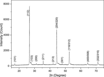
An alloy precursor was deposited on glass by sputtering two targets simultaneously without intentionally heating substrate and selenized at 550 °C for 15 min. Analysis of the precursor by EDS at 20 kV showed the composition to be Cu 48.89 at.%, In 37.41 at.%, Ga 13.70 at.% with Cu/(In + Ga) = 0.96 and Ga/(In + Ga) = 0.27. Figure 2 shows XRD pattern of the sample after selenization. It can be seen that the sample has a basic chalcopyrite crystal structure and shows a preferred orientation of (112) according to Joint Committee on Powder Diffraction Standards (JCPDS) No. 40-1487. Other secondary phase could not be found from the XRD pattern.
XRD pattern of the CIGSe thin film produced by selenizing the Cu–In–Ga alloy precursor, which was sputtering deposited at ambient temperature.

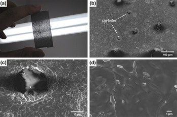
Scanning electron microscopy (SEM) analysis of the CIGSe sample (Fig. 3) shows that a lot of pinholes existed. The diameter of these pinholes is about 10–20 μm. The area beyond holes still exhibits a flat and large grain structure. Considering the reasons for pinholes formation, several process stages were taken into account: (i) preheating stage: pinholes formed in preheating temperature process of 250 °C or before metallic precursor reacted with Se. (ii) Selenization stage: recrystallization and interdiffusion took place during the reactive annealing, which might cause the formation of pinholes. (iii) Cooling stage: the significant difference in thermal expansion coefficients between the film and the substrate would introduce thermal residual stresses, which might give rise to pinholes.
(a) Backlighting photography, (b) surface SEM micrograph, (c) enlarged micrograph of the pinhole, and (d) enlarged micrograph of the area beyond holes of the CIGSe thin film produced by selenizing the Cu–In–Ga alloy precursor, which was sputtering deposited at ambient temperature.

B. Heat treatment of Cu–In–Ga alloy precursors
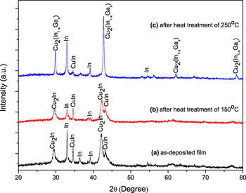
To examine the possibility that pinholes might form in the temperature rise period of selenization process, separate heat treatments of alloy precursors, which were sputtering deposited at ambient temperature, were performed in a Se-free atmosphere, simulating the preheating stage. The heat treatment temperature was set at 150 and 250 °C for 30 min. Some pinholes were also found in these films after heat treatment. It indicates that the pinholes in Fig. 3 might be formed before selenization or before metallic precursor reacted with Se. XRD pattern (Fig. 4) of the sample after heat treatment of 150 °C is almost the same as the as-deposited film, which shows prominent peaks related to Cu2In, CuIn, and In. But no Cu–Ga related peaks were found, what could be explained that Cu–Ga phase mostly existed in low crystallinity. However, after heat treatment at 250 °C, XRD pattern of Cu–In–Ga precursor transforms. The positions of the Cu2In (101) peak (2θ = 29.633°) and (102) peak (2θ = 42.295°) move to higher diffraction angle 2θ = 29.886° and 2θ = 42.773°, respectively, when the heat treatment temperature increased from 150 to 250 °C. According to JCPDS No. 42-1475, the lattice constants for Cu2In with a hexagonal lattice structure are a = 4.2943 Å and c = 5.2328 Å. After cell refinement of Fig. 4(c), precise lattice constants with a = 4.2247 Å and c = 5.1742 Å were determined. It is attributed to the formation of solid solution Cu2(In1−xGax) when Ga atoms occupy In positions based on Cu2In phase structure. Due to the limitation of migration energy of sputtered atoms, the deposited film by sputtering is at metastable state. Under the thermal driving force of annealing, film tends into its lowest energy state.
XRD patterns of Cu–In–Ga alloy precursors, which were sputtering deposited at ambient temperature: (a) the as-deposited film, (b) after heat treatment of 150 °C for 30 min, and (c) after heat treatment of 250 °C for 30 min.

C. Substrate temperature dependence of the properties of Cu–In–Ga alloy precursor
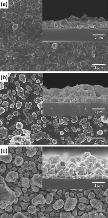
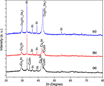
Based on the understanding of initial alloy precursor pinholes formation, specific sputtering substrate temperature was applied. The migration energy of sputtered atoms on substrate depends greatly on the substrate temperature and increases with the increase of substrate temperature. Therefore, increasing substrate temperature may result in films with more steady state. The advantage of sputtering process in attaining uniform thin films could inhibit the formation of pinholes. The dependence of surface morphology on the sputtering substrate temperature for Cu–In–Ga precursors was illustrated by SEM secondary electron image (Fig. 5). It can be seen that the mean surface roughness increased with the increase of sputtering substrate temperature. Moreover, no pinholes were found in these films. Figure 6 reveals the diffraction patterns of the Cu–In–Ga alloy precursors deposited at various sputtering substrate temperatures. When sputtering substrate temperature was 250 °C, the phase compositions of the precursor film were elemental indium and Cu2(In1−xGax) solid solution, which are the same as those of Fig. 4(c). It can be explained that the film entered into a more stable state and could avoid the formation of pinholes in the temperature rise period of selenization process, as evidenced by SEM results.
Surface SEM micrographs and cross-sectional views of alloy precursors, which were sputtering deposited at (a) ambient temperature, (b) 150 °C, and (c) 250 °C.

XRD patterns of Cu–In–Ga alloy precursors, which were sputtering deposited at (a) ambient temperature, (b) 150 °C, and (c) 250 °C.

D. Optimized preparation of CIGSe thin films
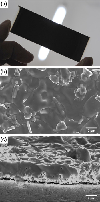
Based on the above analysis, a sputtering substrate temperature of 250 °C was applied to optimize the preparation of the Cu–In–Ga alloy precursors, hence optimizing the preparation of the CIGSe thin films. Figure 7 shows a rather flat, compactly packed, large grain thin film free of pinholes and microcracks. Single chalcopyrite phase was also detected by its XRD pattern. The Cu, In, Ga, and Se concentrations of the CIGSe thin film, determined by XRF, are 24.24, 18.27, 7.45, and 50.04 at.%. Hence, the Cu/(In + Ga) and Ga/(In + Ga) atomic ratio are 0.94 and 0.29, which are nearly equal to those of the metal precursor. The formation of pinholes during selenization can be also connected with the surface roughness of metal precursor, which increased with the increase of sputtering substrate temperature. High compactness of the film is not beneficial to the diffusion of Se vapor and could cause pinholes due to internal stress. It should also be noted that after selenization, the CIGSe film presents a more flat surface as compared to its precursor. It could be explained that the reaction between Cu–In–Ga precursor and Se led to the increase of thickness of film, as evidenced by the comparison of the cross-sectional view of the metal precursor and CIGSe thin film (Figs. 5 and 7). During selenization with high Se vapor pressure, precursor even with high surface roughness could transform to flat CIGSe film.
(a) Backlighting photography, (b) surface SEM micrograph, and (c) cross-sectional view of the CIGSe thin film produced by selenizing the Cu–In–Ga alloy precursor, which was sputtering deposited at 250 °C.

IV. CONCLUSIONS
A two-stage method has been developed to prepare CIGSe absorbers, by combining sputtered-deposited Cu–In–Ga precursors and selenization using Se vapor. Initially, CIGSe absorber was prepared from the Cu–In–Ga alloy precursor, which was sputtering deposited at ambient temperature. The results show that a lot of pinholes existed in the film. Several process stages, which could influence the possibility of formation of pinholes, were analyzed carefully. Separate heat treatment experiments were designed to simulate the preheating stage of selenization process, results of which indicate phase transformation and pinholes formation happened. Based on the understanding of initial alloy precursor pinholes formation, specific substrate temperature of 150 and 250 °C was applied. XRD studies confirm the phase compositions of the precursor film were elemental indium and Cu2(In1−xGax) solid solution when sputtering substrate temperature was 250 °C. SEM studies show that the mean surface roughness increased with the increase of sputtering substrate temperature. A CIGSe absorber with a flat, compactly packed, large grain free of pinholes and microcracks was finally achieved during selenization.
ACKNOWLEDGMENTS
The authors are thankful to Song Jun for equipment maintenance, Dr. Li Zhen for beneficial discussion. This work was financially supported by Initiative Scientific Research Project of Tsinghua University.