Introduction
With the rapid development of multi-standard wireless communication technologies, integrating and converging multiple communication protocols has become a promising trend in microwave filter exploration for system capacity improvement and system volume reduction [Reference Cho, Yun and Park1, Reference Lan, Qu, Guo and Ding2]. The tunable bandpass filter (BPF) based on semi-conductor varactors has become a research hotspot due to its adjustable operating performance and its outstanding characteristics such as rapid agility, minimized system size, the potential for integration, and low cost.
To achieve tunable BPF with independently controlled passbands for receiving system size reduction, several attempts with varactor-loaded planar microstrip resonators are proposed in papers [Reference Li, Du, Chang, Ke and Cai3–Reference Zhou, Zhu and Wu11]. In papers [Reference Li, Du, Chang, Ke and Cai3–Reference Zhang, Wang, Wang, Bai and Shi5], a dual-band filter with one tunable passband and a fixed one can be implemented based on a single multi-mode resonator. Such construction with a single multi-mode resonator rarely achieves dual tunable passband, mainly owing to the restriction of mutually influenced modes within one multi-mode resonator. Though a dual-band tunable filter can be approached by employing an ingenious multi-mode square ring resonator in paper [Reference Pal, Mandal and Dwari6], the two passbands with a flaw of under modified selectivity sideband are not independently controllable because of the mutual influence of the intrinsic resonant modes. To address the limitations of a single multi-mode resonator and realize the independent tunability of a dual-band filter, the structure by combining two sets of multi-mode resonators using a common external coupling feedline achieving independently controlled passbands is given in papers [Reference Wang, Wang, Zhou, Zhang, He and Li7–Reference You, Long, Liang and Xuan10], and the center frequency (CF) and tunable mechanism of the multi-mode resonator are designed respectively. However, there are still non-tunable passbands in papers [Reference Wang, Wang, Zhou, Zhang, He and Li7, Reference Xiang, Chang, Li, Chen and Jian8]. In papers [Reference Chaudhary, Jeong and Lim9, Reference You, Long, Liang and Xuan10], the independent adjustment of dual-band filter is realized by designing the coincide structure of multi-mode resonators working in different frequencies. Moreover, in paper [Reference Zhou, Zhu and Wu11], multi-mode substrate-integrated waveguide (SIW) techniques are also applied to obtain dual-band independent tunable filter with high Q-value characteristics based on a stub-capacitor-loaded half-mode SIW structure.
Unfortunately, many tunable BPFs have been reported, but a few focus on absolute bandwidth characteristics. Tunable BPF without constant absolute bandwidth (CABW) may cause comprehensive deterioration of the reception spectrum in practical applications.
To meet the requirements of constant bandwidth receivers for high S/N sensitivity applications, serval attempts to explore center-frequency-tunable BPF with CABW have been published in papers [Reference Cai, Chen, Zhang, Yang and Bao12–Reference Chen and Chu19]. The tunable filters with single CABW are proposed in papers [Reference Cai, Chen, Zhang, Yang and Bao12–Reference Zhu, Xue, Sun, Liu and Deng17], the bandwidth can be kept constant during the tuning process, and the passband selectivity characteristics were high. Further, dual-band BPF with CABW CF tuning is also presented in paper [Reference Narayana, Kumar and Singh18]. Nevertheless, the independence between two tunable passbands collapses with the raised amount of multiple varactor elements loaded on the multi-mode resonator of the desired dual-band BPF. A dual-band tunable BPF is obtained using a mixed electric/magnetic coupling mechanism [Reference Chen and Chu19]. Although it is achieved independently tunable the two passbands with the CABW feature, the band-to-band isolation needs further modification.
Therefore, to realize compact dual-band BPF with two independent tunability CABW switchable passbands, high selectivity, high level of band-to-band isolation by using multiple adaptive transmission zeros (TZs) of both sidebands of two passbands, and high operating frequency reaching 3.8 GHz for 5G application is still a challenge.
In this paper, a novel tunable and switchable dual-band BPF with independently controlled passbands and CABW with four self-adaptive zeros is presented. In the proposed tunable filter, multiple transmission paths were implemented based on a varactor-loaded resonator, coupled 1/4λ wavelength varactor-loaded resonator and shorted coupled feedlines. Due to multiple transmission path cancellation techniques between the input port to the output port and the virtual short mechanism at a specific frequency, two pairs of adaptive TZs were successfully planted at both the lower and upper sideband of two passbands. Therefore, enhanced selectivity and isolation of two passbands developed without extra circuit size. Additionally, independent controllable and switchable characteristics are approached owing to the independently designed two transmission paths for the lower passband and upper passband. Moreover, properly managing intrinsic discrete electric magnetic coupling of varactor loaded resonator and coupled 1/4λ wavelength varactor loaded resonator, the characteristic of the CABW also fulfilled in the proposed filter. To verify the afore-demonstrated design methodologies, a prototype filter of 2.38–2.68 GHz tunable first passband with 101 MHz CABW and 3.28–3.88 GHz tunable second passband with 98 MHz CABW filter is designed, implemented, and tested and prove that the maximum operating frequency can reach 3.8 GHz for 5G applications. The core innovation of this article is owing to the proposed independently tunable and independently switchable BPF can achieve constant bandwidth with whole tuning range up to 5G band. The proposed manuscript is the first to implement such functionality, as far as we know. Further, the proposed dual-band BPF also has the advantages of independent control of passband voltage, high selectivity, and band-to-band isolation.
This paper is organized as follows. First, the characteristics of proposed tunable resonators are discussed in section Theoretical analysis and filter design. Second, the design and implementation of the filter, along with the simulated and measured results, are described in Section Design and implementation of the proposed BPF. Finally, conclusions are drawn in Section Conclusion.
Theoretical analysis and filter design
In this section, the design of the tunable dual-band BPFs with CABW is proposed and designed. The schematic diagram of the proposed filter is provided in Fig. 1(a). In the proposed filter, multiple transmission paths can be separated by a pair of shorted transmission lines loaded with a varactor, a varactor-tuned stub-loaded resonator (SL-SIR), and a pair of shorted parallel coupling lines (SPCLs). Figure 1(a) shows that the blue-colored shorted transmission line loaded with varactor is of path I and yields the lower passband. The purple-colored varactor-tuned SL-SIR is of path II and generates the higher passband. SPCL is of path III which contributes multiple TZs.
Proposed BPF. (a) Schematic diagram and (b) coupling routing scheme.

As depicted in Fig. 1(b), S and L denote input and output ports separately. The nodes represented with numbers 1–4 stand for resonant modes. Herein, 1 and 2 correspond to two modes that create the first passband, while 3 and 4 denote two modes of SL-SIR, which construct the second passband. Therefore, the two passbands are designed independently and have no mutual influence on each other. The two passbands are investigated as follows.
Resonator theoretical analysis
Design methodology of path I
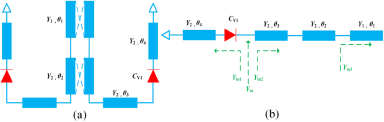
Figure 2(a) shows that a pair of shorted transmission line loaded varactor C V1 through parallel coupling achieves the first passband. Figure 2(b) depicts the resonator’s equivalent circuit.
(a) Proposed short circuit transmission line loaded varactor and (b) equivalent TLM.

The input admittance is given by
 \begin{equation}\begin{array}{*{20}{c}}
{{Y_{{\text{in1}}}}{\text{ = }}\frac{{{{2\pi }}f{C_{{\text{V1}}}}{Y_{\text{2}}}{\text{cot}}{\theta _{\text{4}}}}}{{{{j2\pi }}f{C_{{\text{V1}}}} - {\text{j}}{Y_{\text{2}}}{\text{cot}}{\theta _{\text{4}}}}}{\text{ = }}\;{\text{j}}{Y_{\text{2}}}\frac{{{{2\pi }}f{C_{{\text{V1}}}}}}{{{Y_{\text{2}}} - {{2\pi }}f{C_{{\text{V1}}}}{\text{tan}}{\theta _{\text{4}}}}}}
\end{array}\end{equation}
 \begin{equation}\begin{array}{*{20}{c}}
{{Y_{{\text{in3}}}}{\text{ = j}}{Y_{\text{1}}}{\text{tan}}{\theta _{\text{1}}}}
\end{array}\end{equation}
 \begin{equation}\begin{array}{*{20}{c}}
{{Y_{{\text{in2}}}} = {Y_2}\frac{{{Y_{{\text{in3}}}} + {\text{j}}{Y_2}\tan ({\theta _2} + {\theta _3})}}{{{Y_{\text{2}}} + {\text{j}}{Y_{{\text{in3}}}}\tan ({\theta _2} + {\theta _3})}} = {\text{j}}{Y_2}\frac{{{Y_1}\tan {\theta _1} + {Y_2}\tan ({\theta _2} + {\theta _3})}}{{{Y_2} - {Y_1}\tan {\theta _1}\tan ({\theta _2} + {\theta _3})}}}
\end{array}\end{equation}
 \begin{equation}\begin{array}{*{20}{c}}
{{Y_{{\text{in}}}} = {Y_{{\text{in1}}}} + {Y_{{\text{in2}}}}}
\end{array}\end{equation}
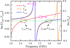
where f denotes the reference frequency. When the resonant condition Im (Y in) = 0 is satisfied, two resonant frequencies f 1-A and f 1-B can be derived. It can be observed from Equations (1–4) that f 1-A and f 1-B can be changed by varying C V1. The electrical lengths and characteristic admittances of the ideal transmission line model (TLM) are respectively denoted by  $\,{{{\theta}}_{\text{i}}}\,$ and Yi, i = 1, 2, 3, …, respectively. Here, θi = βLi, and β is the propagation constant of the microstrip line.
Design methodology of path II
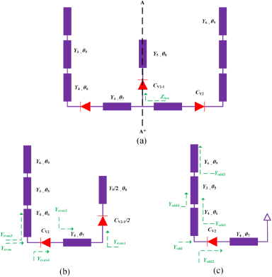
The second band is achieved by a varactor-tuned SL-SIR. As indicated in Fig. 3(a), the proposed resonator basic TLM is presented. Due to the SL-SIR being symmetrical with plane A-A*, the classical odd-even mode method can be employed to analyze the proposed resonator.
(a) Proposed SL-SIR TLM, (b) even-mode equivalent circuit, and (c) odd-mode equivalent circuit.

The equivalent circuit is shown in Fig. 3(b) for the even-mode excitation.
The equivalent circuit is shown in Fig. 3(c) for the odd-mode excitation.
The following equations can derive the input admittances of the odd-even mode excitation:
 \begin{equation}\begin{array}{*{20}{c}}
{{Y_{{\text{odd3}}}} = {\text{j}}{Y_6}{\text{tan}}{\theta _{\text{9}}}}
\end{array}\end{equation}
 \begin{equation}\begin{array}{*{20}{c}}
{{Y_{{\text{odd4}}}} = {\text{j}}{Y_3}\frac{{{Y_{{\text{odd3}}}} + {\text{j}}{Y_3}\tan {\theta _5}}}{{{Y_3} + {\text{j}}{Y_{{\text{odd3}}}}\tan {\theta _5}}}}
\end{array}\end{equation}
 \begin{equation}\begin{array}{*{20}{c}}
{{Y_{{\text{odd1}}}} = {Y_4}\frac{{{Y_{{\text{odd4}}}} + {\text{j}}{Y_4}\tan {\theta _6}}}{{{Y_4} + {\text{j}}{Y_{{\text{odd4}}}}\tan {\theta _6}}}}
\end{array}\end{equation}
 \begin{equation}\begin{array}{*{20}{c}}
{{Y_{{\text{odd2}}}} = \frac{{2\pi f{C_{{\text{V2}}}}{Y_4}\cot {\theta _7}}}{{{\text{j}}2\pi f{C_{{\text{V2}}}} - {\text{j}}{Y_4}\cot {\theta _7}}} = {\text{j}}{Y_4}\frac{{2\pi f{C_{{\text{V2}}}}}}{{{Y_4} - 2\pi f{C_{{\text{V}}2}}\tan {\theta _7}}}}
\end{array}\end{equation}
 \begin{equation}\begin{array}{*{20}{c}}
{{Y_{{\text{odd}}}} = {Y_{{\text{odd1}}}} + {Y_{{\text{odd2}}}}}
\end{array}\end{equation}
 \begin{equation}\begin{array}{*{20}{c}}
{{Y_{{\text{even1}}}} = \frac{{{\text{j}}\pi f{C_{{\text{V2 - 1}}}}*{\text{j}}{Y_5}\tan {\theta _8}/2}}{{{\text{j}}\pi f{C_{{\text{V2 - 1}}}} + {\text{j}}{Y_5}\tan {\theta _8}/2}} = {\text{j}}{Y_5}\frac{{\pi f{C_{V2 - 1}}\tan {\theta _8}}}{{{Y_5}\tan {\theta _8} + 2\pi f{C_{{\text{V2 - 1}}}}}}}
\end{array}\end{equation}
 \begin{equation}\begin{array}{*{20}{c}}
{{Y_{{\text{even2}}}} = {Y_4}\frac{{{Y_{{\text{even1}}}} + {\text{j}}{Y_4}\tan {\theta _7}}}{{{Y_4} + {\text{j}}{Y_{even1}}\tan {\theta _7}}}}
\end{array}\end{equation}
 \begin{equation}\begin{array}{*{20}{c}}
{{Y_{{\text{even3}}}} = {Y_{{\text{odd1}}}} = {Y_4}\frac{{{Y_{{\text{odd4}}}} + {\text{j}}{Y_4}\tan {\theta _6}}}{{{Y_4} + {\text{j}}{Y_{{\text{odd4}}}}\tan {\theta _6}}}}
\end{array}\end{equation}
 \begin{equation}\begin{array}{*{20}{c}}
{{Y_{{\text{even4}}}} = \frac{{{\text{j}}2\pi f{C_{{\text{V2}}}}{Y_{{\text{even2}}}}}}{{{\text{j}}2\pi f{C_{{\text{V2}}}} + {Y_{{\text{even2}}}}}}}
\end{array}\end{equation}
 \begin{equation}\begin{array}{*{20}{c}}
{{Y_{{\text{even}}}} = {Y_{{\text{even3}}}} + {Y_{{\text{even4}}}}}
\end{array}\end{equation}
where  ${\textbf{\it{\,}}}f$ denotes the reference frequency. When the resonant condition Im (Y odd) = 0 and Im (Y even) = 0 is satisfied, two resonant frequencies f 2-even and f 2-odd can be extracted by Equations (5–14). It can be observed from Equations (5–14) that odd-mode resonant frequency f 2-odd can be independently tuned by probably changing the value of C V2, and the even-mode resonant frequency f 2-even can be shifted by appropriately selecting the bias of varactors with an identical voltage of C V2 and C V2-1. By reasonably choosing the electrical parameters of the θ 8, synchronous variations of f 2-even and f 2-odd of the second passband can be implemented, and single bias voltage fulfills the requirement of tunable second passband.
Moreover, a transmission zero TZ4 is introduced due to the open stub loaded with C V2-1, to analyze the position of the TZ, and the input impedance of the open stub loaded with the varactor C V2-1 can be derived with the help of the following equations:
 \begin{equation}\begin{array}{*{20}{c}}
{{Z_{\text{in}}\alpha} = - \frac{{2\pi f{C_{{\text{V2 - 1}}}}{Y_5}\tan {\theta _8}}}{{{\text{j}}2\pi f{C_{{\text{V2 - 1}}}} + j{Y_5}\tan {\theta _8}}} = {\text{j}}\frac{{2\pi f{C_{{\text{V2 - 1}}}}{Y_5}\tan {\theta _8}}}{{2\pi f{C_{{\text{V2 - 1}}}} + {Y_5}\tan {\theta _8}}}}
\end{array}\end{equation}
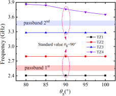
It is observed that the frequency of transmission zero TZ4 can be deduced when the condition of  ${Z_{{\text{in}}\alpha}} = 0$ is satisfied, which indicates that TZ4 can be adjusted by varied C V2-1 and changing the value of θ 8. Figure 4 sketches the TZs versus the varied value of
 ${\theta _{\text{8}}},{ }$thus revealing that the larger
 ${\theta _{\text{8}}}$, the decliner TZ4.
Transmission zero position against different  ${\theta _{\text{8}}}\,$ of path II.

Figure 5 depicts the input admittance imaginary part Y in of path I and the odd-even mode input admittance Y even and Y odd of path II of the proposed filter. When the admittance imaginary part is zero, it can be extracted that the resonant mode of the path I is located at the CF 2.52 GHz of the designed first passband. Similarly, the odd-mode and even-mode resonant frequencies of path II are set at 3.62 GHz to yield the second passband.
The imaginary part of input admittance Im (Y in), Im (Y odd), and Im (Y even) versus the range of design passband.

Design methodology of path III
In addition, thanks to the implementation of the proposed path III structure, three extra TZs are introduced, which can be self-adaptive shifted with varied centered frequencies of two passbands. Figure 6 extracted the influence of path III on the transmission characteristics in the case of weak coupling. It can be easily found that multiple transmission cancellations cause TZ1, TZ2, and TZ3 by introducing path III, while TZ4 is caused by a virtual short-out mechanism when Z inα = 0 at a specific frequency.
The magnitude of weakly coupled frequency responses |S21| with path III and without path III.

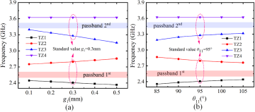
Figure 7 depicts the impact of different parameters of path III on the transmission zero TZ1, TZ2, and TZ3 position. It is observed that the frequency of transmission zero TZ1, TZ2, and TZ3 can be adjusted by varying the values of g 1 and θ 11. Based on Figs. 4 and 7, with enlarged g 1 and declined θ 8, each of two TZs located at the upper and lower sidebands of two passbands are both widened to match varied bandwidths to obtain a sharp skirt of two passbands.
(a) Transmission zero position against different g 1 of path III. (b)Transmission zero position against different  ${\theta _{{\text{11}}}}$ of path III.

The simulated current distribution at two centered frequencies f 1 and f 2 of two passbands are illustrated in Fig. 8. It can be drawn from Fig. 8 that the current distributions mainly concentrate at path I at CF of the first passband f 1 at 2.52 GHz, and the current distributions mainly concentrate at path II at CF of the second passband f 2 at 3.62 GHz. Compared to employing variable capacitors as equivalent circuit models for varactor analysis, in full-wave electromagnetic simulation, we further introduced a precisely equivalent varactor model with input resistance and parasitic inductance components, as shown in Fig. 9.
The current distributions (a) at the first passband centered frequency f 1 and (b) at the second passband centered frequency f 2.

Equivalent circuit model of varactor diode.

According to the analysis of the proposed resonator above, it can be concluded that C V1 only affects the first passband resonant frequency f 1 and C V2 only affects the second passband resonant frequency f 2. The dual-band filter with independently tunable passbands can be, therefore, designed by combination with multiple transmission paths. By controlling voltages V 1 and V 2, the two passbands can be tuned independently.
Constant bandwidth requirement
For the CABW filter, the relationships between CABW and coupling coefficient K 12, external quality factor Qe are expressed as follows:
 \begin{equation}\begin{array}{*{20}{c}}
{{K_{12}} = \frac{{ABW}}{{{f_0}\sqrt {{g_1}{g_2}} }}}
\end{array}\end{equation}
 \begin{equation}\begin{array}{*{20}{c}}
{{Q_e} = \frac{{{f_0}{g_1}{g_2}}}{{ABW}}}
\end{array}\end{equation}
where f 0 and ABW, respectively, represent the passband CF and absolute bandwidth, g 0, g 1, and g 2 are the 2nd-order element values of the low-pass prototype filter network. According to Equations (16) and (17), to achieve the CABW, the inverse variation trends of coupling coefficient K 12 and centered frequency should be achieved. Meanwhile, consistent changing trends of Q e and centered frequency need to be approached.
To verify the theoretical analysis, the initial values of the parameters are assumed as follows: θ 1 = θ 2 = θ 5 = 10°, θ 3 = θ 4 = θ 7 = θ 8 = 20°, θ 9 = θ 10 = 30°, 2θ 6 = θ 11 = 120° and Z 8 = 60 Ω, 3Z 1 = 3Z 4 = Z 3 = Z 5 = Z 7 = 90 Ω, Z 2 = Z 6 = 120 Ω, Yi = 1/Zi.
Coupling coefficient K12
We extracted the various coupling coefficients versus varied electrical parameters and physical dimensions according to the following formula:
 \begin{equation}\begin{array}{*{20}{c}}
{{K_{12}} = \frac{{f_{1 - {\text{A}}}^{\,\,2}\, - \,\,f_{1 - {\text{B}}}^{\,\,2}}}{{f_{1 - {\text{A}}}^{\,\,2}\, + \,\,f_{1 - {\text{B}}}^{\,\,2}}}}
\end{array}\end{equation}
 \begin{equation}\begin{array}{*{20}{c}}
{{K_{12}} = \frac{{f_{2 - {\text{even}}}^{\,\,2} - \,f_{2 - {\text{odd}}}^{\,\,2}}}{{f_{2 - {\text{even}}}^{\,\,2} + \,f_{2 - {\text{odd}}}^{\,\,2}}}}.
\end{array}\end{equation}
Figure 10(a) and (b) depicts the numerical calculated resonant frequency f 1 and coupling coefficient K 12 for the first passband with different  ${\theta _{\text{2}}}$ and g 2, respectively, representing the electrical length of the coupling line and the distance between parallel coupled lines. It can be concluded that the coupling coefficient K 12 is mainly influenced by
 ${\theta _{\text{2}}}$ and g 2. Similarly, the resonant frequency f 2 and coupling coefficient K 12 for the second passband under different values of open stub length
 ${\theta _{\text{8}}}$ can also be derived and demonstrated in Fig. 10(c).
(a) Extracted K 12 of the first passband against different  ${\theta _{\text{2}}}$, (b) extracted K 12 of the first passband against different g2, and (c) extracted K 12 of the second passband against different
 ${\theta _{\text{8}}}$.

External quality factor Qe
The external quality factor Qe for each designed passband can be derived as follows:
 \begin{equation}\begin{array}{*{20}{c}}
{{Q_e} = \pi {f_0}{\tau _{S11}}}
\end{array}\end{equation}
where  ${{{\tau }}_{{\text{S11}}}}$ is the group delays of S 11 at the CF of each passband. The desired external quality factor Qe of the designed centered frequency of path I can be fulfilled by appropriately choosing the coupling strength of feed lines and the electrical value
 ${\theta _{\text{4}}}$ of paralleled coupled lines. Herein, the coupling strength of path I is mainly affected by
 ${\theta _{\text{4}}}$ and gap dimension s 1, as illustrated in Fig. 11(a) and (b), whereas the gap distance s 2 can be independent effects the external quality factor Qe of path II to cater for the required design specification of the second passband. The detailed extracted Qe of path II versus variation of s 2 is portrayed in Fig. 11(c).
(a) Extracted Qe of the first passband against different  ${\theta _{\text{4}}}$, (b) extracted Qe of the first passband against different s 1, and (c) extracted Qe of the second passband against different s 2.

It can be seen from Figs. 10 and 11 that the external factor Qe increases with enlarged frequencies, while the coupling coefficient K 12 declines with increased frequencies, which agrees with the theory analysis.
According to the afore-demonstrated design graphs, by appropriately selecting the values of electrical values and gap distance of each transmission path, the CABW can be realized. Therefore, tunable and switchable CABW dual-band BPF is approached.
The design methodology procedure is summarized as a flowchart in Fig. 12. The presented filter design methodology consists of two steps.
Design procedure of proposed CABW BPF.

Step I: According to resonant theoretical analysis and designing specifications, complete the passband design for path I and path II. By properly selecting L 11, W 7, and g 1 to further improve the selectivity of each sideband of two passbands. Thus, L 1, L 2, L 3, L 4, L 6, L 7, L 8, L 9, L 11, W 1, W 2, W 3, and W 4 can be determined.
Step II: Complete the selection of varactor diode type based on the desired tuning range; Accomplish the design of DC bias and Radio Frequency (RF) isolation circuits. To achieve CABW within the whole tuning range, the construct required K 12 and Q e according to Figs. 10 and 11. Thus far, all the electrical parameters of the filer determined.
Therefore, tunable and switchable CABW dual-band BPF is approached.
Design and implementation of the proposed BPF
To verify the design methodology, a prototype tunable dual-band filter was designed, simulated, and measured. It is fabricated on a Rogers RO4003C substrate with a relative dielectric of 3.55 and thickness of 0.508 mm. The physical dimensions of the prototype dual-band BPF are optimized by the Electronic Magnetic (EM) full-wave simulator as follows. L 1 = 0.8 mm, L 2 = 2.4 mm, L 3 = 4.15 mm, L 4 = 5.65 mm, L 5 = 2.7 mm, L 6 = 9.7 mm, L 7 = 5.8 mm, L 8 = 4.3 mm, L 9 = 7.85 mm, L 10 = 5.95 mm, L 11 = 19.95 mm, L 12 = 2.41 mm, W 1 = 1.7 mm, W 2 = 0.25 mm, W 3 = 0.3 mm, W 4 = 0.7 mm, W 5 = 0.3 mm, W 6 = 0.15 mm, W 7 = 0.4 mm, W 8 = 1.1 mm, W 9 = 0.1 mm, g 1 = 0.3 mm, g 2 = 0.4 mm, s 1 = 0.3 mm, s 2 = 0.2 mm, s 3 = 0.8 mm. The effective circuit size occupies 16 mm × 22 mm or 0.20λ g × 0.28λ g (λ g is the guided wavelength of 50 Ω microstrip lines at the CF of the first passband f 1). The photograph of the fabricated tunable BPF is given in Fig. 13.
The photograph of the fabricated tunable dual-band BPF.

The varactor diode C V1 is Skyworks SMV1234 with a specified capacitance of 1.32–9.63 pF at 0–15 V bias voltages, and the varactor diode C V2 is Skyworks SMV1233 with a specified capacitance of 0.84–5.08 pF at 0–15 V bias voltages, which can be managed by varied bias voltages of V 1 and V 2, respectively. In this paper, the simulation and measurement are, respectively, characterized by EM full-wave simulator Sonnet and Agilent network analyzer E5071C.
Figure 14 shows the simulated and measured results of the proposed filter for several typical bias voltages. The solid line represents the simulation results, and the dashed line represents the measurement results. We can draw from Fig. 14(a) and (b) that the first passband CF can be tuned from 2.38 to 2.68 GHz with varied bias voltage V 1 from 1.9 to 11 V, while the second passband remains unchanged with a whole tuning range of the first passband, the 3-dB absolute bandwidth of the first passband is 101 ± 7 MHz. Similarly, as can be observed from Fig. 14(c) and (d), when the bias voltage V 2 varies from 1.1 to 14.9 V, the second passband CF can be tuned from 3.28 to 3.88 GHz, whereas the first passband remains unchanged, the second passband 3-dB absolute bandwidth is 98 ± 4 MHz.
The simulation and measurement results of the proposed filter for several typical bias voltages. The solid line represents the simulation results, and the dashed line represents the measurement results. (a) The results of S21 with tunable first passband and fixed second passband (V 2 = 3.3 V and V 1 = 1.9–11 V), (b) the results of S11 with tunable first passband and fixed second passband (V 2 = 3.3 V and V 1 = 1.9–11 V), (c) the results of S21 with tunable second passband and fixed first passband (V 1 = 4.1 V and V 2 = 1.1–14.9 V), and (d) the results of S11 with tunable second passband and fixed first passband (V 1 = 4.1 V and V 2 = 1.1–14.9 V).

We can see from the figures that the measured results agree with the simulated results. The differences between simulated and measurement results are mainly owing to the fabrication tolerances and inconsistency of surface-mounted technology of multiple weld pads. The simulated and measured results of absolute bandwidth and insertion losses with different operation frequencies are indicated in Fig. 15. In addition, in total, four TZs can be found in the simulated measurements, below and above each of the two passbands there is one TZ, respectively.
The simulation and measurement results of absolute bandwidth and insertion loss value at different frequencies. The solid line represents the simulation results, and the dashed line represents the measurement results. (a) The first passband and (b) the second passband.

Figure 16(a) and (b) demonstrates the measured results and simulated results of the switchable characteristics of the presented filter. By controlling the bias voltage imposed on the varactor V 1 and V 2, the passbands without bias voltage can automatically be closed, as shown in Fig. 16(a) and (b). The first passband can be turned off by removing the bias voltage imposed on C V1 while the second passband keeps unchanged. Similarly, the second passband can be shut off by removing the bias voltage imposed on C V2 and the first passband remains constant. Therefore, the proposed tunable dual-band BPF can be switchable independently.
Frequency responses of switchable characteristics. The solid line represents the simulation results, and the dashed line represents the measurement results. (a) The second passband turn-off and (b) the first passband turn-off.

Table 1 summarizes the comparison of this filter with the previous related tunable filters. It shows that the proposed dual-band BPF has the advantages of CABW with the whole tunable range of dual-band filter, and single bias voltage for each tunable passband, independent tunable and switchable characteristics, and up to 3.8 GHz of operating frequency for 5G application.
Comparison between this work and previous tunable BPFs

NM: not mentioned; NT*: not tunable; VAB*: variable absolute bandwidth; ICP: independent controllable of two passbands; NOBV: number of bias voltages required per passband; CABW: passband 1st/passband 2nd (MHz); √: yes; ×: no; Q eff: effective quality factor.
Conclusion
In this paper, a tunable and switchable dual-band BPF with independently controlled passbands and CABW is presented. The SIR and multi-mode resonator with loaded varactor are constructed for a tunable dual-band BPF with unique imposed bias voltage for each passband. By varying the bias voltage imposed on the varactors, two passbands of the filter can be tunable and switchable independently. The detailed design methodology and tunable mechanism have been investigated in this paper. In addition, the bandwidth of the passband remains constant in the whole tuning range of frequency. Simulated and measured results are in good consistency to prove the validity. Measured results confirm simulation predictions well that the proposed filter can be tuned and switched indecently. Moreover, the presented tunable filter has features of multiple adaptive TZs, minimized circuit size, and high operation frequency for 5G mobile applications.
Data availability statement
All data are open for access, please contact the corresponding author Lirong Qian. Lirong Qian, https://orcid.org/0000-0001-9909-4673.
Acknowledgements
This work is supported by National Key R&D Program of China (Grant No. 2022YFA1204602); Guangzhou Key Research & Development Program, Major Science and Technology Projects (Grant No. 202206070001); Research and Development Program in Significant Area of Guangdong Province (Grant No. 2020B0101040002), and Youth Innovation Promotion Association, Chinese Academy of Sciences (Grant No. 2022024). The datasets generated during and/or analyzed during the current study are available from the corresponding author upon reasonable request.
Author contributions
Lirong Qian, Litian Wang, and Honglang Li contributed to the conception of the study. Jing Guo and Litian Wang optimized the simulation design and performed the experiment. Jing Guo, Lirong Qian, Litian Wang, and Cuiping Li contributed significantly to the data analysis and manuscript preparation. Jing Guo and Litian Wang wrote the first draft of the manuscript. Lirong Qian, Cuiping Li, Yahui Tian, and Honglang Li provided critical revision of the manuscript. All authors commented on previous versions of the manuscript and read and approved the final manuscript.
Competing interests
The authors report no conflict of interest.
The authors declare that they have no known competing financial interests or personal relationships that could have appeared to influence the work reported in this paper.

Jing Guo was born in Yulin, Inner Shaanxi province, China. He received a B.E. degree from Xi’an University of Posts and Telecommunications, Xi’an, China, in 2021. He is currently working toward an M.E. degree at Tianjin University of Technology, Tianjin, China. His main research interest is tunable filters.

Lirong Qian received a Ph.D. degree in physical electronics from Tianjin University, Tianjin, China, in 2018. He is currently an assistant professor with the Tianjin Key Laboratory of Film Electronic and Communication Devices, School of Integrated Circuit Science and Engineering, Tianjin University of Technology, Tianjin, China. His research interests include RF MEMS, microacoustic resonators, filters, and sensors.

Litian Wang was born in Tianjin, China, in 1991. He received his Ph.D. degree from Nankai University, Tianjin, China, in 2020. In 2020, he joined Tianjin University of Technology. He is currently an assistant professor and deputy director of the Department School of Integrated Circuit Science and Engineering, Tianjin University of Technology, Tianjin, China. His current research interests include microwave passive devices and systems, high-temperature superconducting circuits, RF integrated circuits, and sensors.

Cuiping Li received her Ph.D. degree in physical electronics from Tianjin University, Tianjin, China, in 2012. She is currently an associate professor with the School of Integrated Circuit Science and Engineering, Tianjin University of Technology, Tianjin, China. Her main research interests are in the fields of surface acoustic wave devices and sensor.

Yahui Tian was born in Shandong Province, China, in 1990. She received her B.S. degree from Shandong University, China, in 2012 and her Ph.D. degree from the Institute of Acoustics, Chinese Academy of Sciences in 2017. Now she is an associate researcher at the Institute of Acoustics, Chinese Academy of Sciences. She has published more than 40 academic papers. Her current research focuses on phononic crystals and surface acoustic wave devices. She has hosted and participated in many National Key R&D Projects, National Natural Fund Project, National Natural Fund Youth Fund, and so on. She has won a classical Chinese Mathematics Artificial Intelligence Science and Technology Award and has been elected to the Beijing Municipal Science and Technology Star.

Honglang Li was born in Hubei Province, China, in 1976. He received his B.S. degree in microelectronics from Hunan University, China, in 1998 and a Ph.D. degree in Acoustics from the Institute of Acoustics, Chinese Academy of Sciences in 2003. From 2003 to 2005, he joined the Venture Business Laboratory, at Chiba University, as a post-doctoral fellow. He is currently a researcher at the National Center for Nanoscience and Technology. His research interests include simulation and application of surface acoustic wave filters and sensors of physical/chemical/biological.