1. INTRODUCTION
Traditional pulsed generators of mega-volt-mega-ampere levels employ schemes with primary capacitive storage and a few power compression stages. This technology counts for about 30 years of investigations and there are many installations worldwide (Bennett et al., Reference Bennett, Sinars, Wenger, Cuneo, Adams, Barnard, Beutler, Burr, Campbell, Claus, Foresi, Johnson, Keller, Lackey, Leifeste, McPherson, Mulville, Neely, Rambo, Rovang, Ruggles, Porter, Simpson, Smith and Speas2006; Li et al., Reference Li, Yuan, Zhang, Shu and Zhang2008; Liu et al., Reference Liu, Yin, Ge, Zhan, Chen, Feng, Shu, Zhang and Wang2007; Liu, Reference Liu, Zou, Wang, He and Zeng2008 and references therein). Main drawbacks of such an approach are the large amount of intermediate elements (water or oil filled intermediate storage capacitances, pulse forming lines, switches on full output voltage, vacuum transmission lines), large dimensions, and complex infrastructure for operation and maintenance. High current linear induction accelerators (LIA) were introduced in the United States (Christofilos et al., Reference Christofilos, Hester, Lamb, Reagan, Sherwood and Wright1964) and in the Soviet Union (Anatskii et al., Reference Anatskii, Bogashev, Bukaev, Yakhruskin, Malyshev, Nalivaika, Pavlovskii, Suslov and Khalchitski1966; Pavlovskii et al., Reference Pavlovskii, Bossamykin, Kuleshov, Gerasimov, Tananakin and Klementiev1975). Recently, a number of applications and improvements of this technology have been reported (Merle et al., Reference Merle, Bombardier, Delvaux, Mouillet, Pierret, Ribes and Vermare2002; Ekdahl et al., Reference Ekdahl, Abeyta, Aragon, Archuleta, Bartsch, Bender, Briggs, Broste, Carlson, Eversole, Frayer, Gallegos, Harrison, Hughes, Jacquez, Johnson, Johnson, McCuistian, Montoy, Mostrom, Nath, Oro, Rowton, Sanchez, Scarpetti, Schauer, Schulze, Tang, Tipton and Tom2006; Bogdan et al., Reference Bogdan, Karas, Kornilov and Manuilenko2008). The main application of linear induction accelerators has been the generation of pulsed high-current electron and ion beams for radiography, fusion, and high energy density experiments. Laser acceleration of intense collimated electron and ion beams are an alternative promising approach (Mangles et al., Reference Mangles, Walton, Najmudin, Dangor, Krushelnick, Malka, Manclossi, Lopes, Carias, Mendes and Dorchies2006; Zhou et al., Reference Zhou, Yu and He2007; Chen et al., Reference Chen, Unick, Vafaei-Najafabadi, Tsui, Fedosejevs, Naseri, Masson-Laborde and Rozmus2008), although the total number of particles in the laser generated beams is still very low (Antici et al., Reference Antici, Fazi, Lombardi, Migliorati, Palumbo, Audeber and Fuchs2008). In an induction accelerator, the beam energy is built up by incrementally accelerating the particles through a number of gaps. In existing induction linacs, up to several hundred gaps are used to obtain final beam energy of tens of MeV. The number of gaps is limited by beam losses and by increases in the beam emittance due to instabilities (Miller et al., 1987). Theory of the LIA operation is considered in detail by Humphries (Reference Humphries1986) and historical development of the LIA family is given by Ekdahl (Reference Ekdahl2002). The most powerful machine of this type is the Russian LIA-30 accelerator on 40 MeV and 100 kA (Pavlovskii et al., Reference Pavlovskii, Bossamykin, Gerasimov, Tananakin, Fedotkin, Morunov, Basmanov, Skripka, Tarasov, Gordeev, Grishin, Anfinogenov, Gritsyna, Averchenkov, Lazarev, Gorkunov, Veresov, Koshelev and Odintsov1998).
Induction voltage adders (IVA) are similar in topology to induction accelerators, except that the central metal conductor is employed to sum-up the voltages produced by induction cells, instead of the electron or ion beam in the LIA (Smith, Reference Smith2004; Yatsui et al., Reference Yatsui, Shimiya, Masugata, Shigeta and Shibata2005). In Hermes III, 80 individual 1.1-MV, 220-kA pulses are generated and added in groups of four to develop 20 1-MV, 730-kA pulses, which are then fed through inductively isolated cavities, and added in series by a magnetically insulated transmission line (Ramirez et al., Reference Ramirez, Prestwich, Johnson, Corley, Denison, Alexander, Franklin, Pankuch, Sanford, Sheridan, Torrison and Zawadzkas1989). This accelerator represents a new generation in design that combines conventional modular pulsed power technology with induction voltage adder techniques, and magnetically insulated vacuum line technology to achieve both high voltage and high current with fast rise times, and short pulse widths (Sanford, Reference Sanford1991). Large induction accelerators and voltage adders make use of Marx generators and intermediate pulse forming lines in order to deliver energy to the accelerator sections. Linear transformer driver (LTD) technology was pioneered by the Institute of High Current Electronics in Russia (Kovalchuk et al., Reference Kovalchuk, Vizir, Kim, Kumpjak, Loginov, Bastrikov, Chervyakov, Tsoy, Monjaux and Huet1997, Reference Kovalchuk, Kim, Kumpjak and Tsoy1999). In linear transformer driver technology, capacitors and switches are directly incorporated in the individual cavities (called stages) to generate a fast output voltage pulse that is added along a vacuum coaxial line-like in an IVA. Further development of the LTD technology is described in the literature (Bastrikov et al., Reference Bastrikov, Vizir, Volkov, Durakov, Efremov, Zorin, Kim, Kovalchuk, Kumpyak, Loginov, Sinebryukhov, Tsou, Chervyakov, Yakovlev and Mesyats2003; Mazarakis et al., Reference Mazarakis, Fowler, McDaniel, Olson, Sonrisa, Struve, Stugar, Kim and Sinebryukhov2007). LTD based drivers are currently considered for many applications, including high current Z-pinch drivers (Stygar et al., Reference Stygar, Cuneo, Headley, Ives, Leeper, Mazarakis, Olson, Porter, Wagoner and Woodworth2007), medium current drivers with adjustable pulse length for isentropic compression experiments (Kovalchuk et al., Reference Kovalchuk, Kumpjak, Tsoi, Kim, Avrillaud, Courtois, Guerre, Hereil, Lassalle, Bayol and L'Eplattenier2003), and relatively low current accelerators for radiography (Rose et al., Reference Rose, Welch, Oliver, Leckbee, Maenchen, Johnson, Kim, Kovalchuk and Sinebryukhov2006), and X-pinches (Kharlov et al., Reference Kharlov, Kovalchuk and Zorin2006). In this article, we describe a new LTD stage, which can be used as a modular element in design of multi-MV and multi-MA generators. There are a few main improvements in the new stage in comparison with the earlier developed ones: (1) Atmospheric air is used both as insulation in the generator and as a working gas in the spark gap switches. (2) Implementation of new capacitors and improvement of the switch technology allowed us to increase charging voltage and stored energy density. (3) Modular configuration, employed in the LTD design, ensures easy handling and maintenance (each module can be taken out without disassembling of the whole installation).
2. STAGE DESIGN
The stage includes four modules and each module consists of five capacitor blocks, connected in parallel. The total stage capacitance is equal to 1.6 µF. The LTD stage stores 8 kJ of energy at 100 kV charging voltage. Stage footprint is 290 × 295 cm2, the height is 13 cm.
2.1. Capacitor Blocks of the Transformer Stage
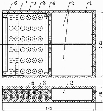
The capacitor block is the main structural element of the generator. Design of the capacitor block is given in Figure 1. It incorporates two capacitors GA 35426 (40 nF, 100 kV) and multi-channel multi-gap gas switch. Body (1) of the block is made from epoxy-silica sand compound. Capacitors (2) are cast in the block body (1). The casting allows an increasing of charging voltage up to 100 kV in atmospheric air. Terminals of the capacitors are connected to the switch high voltage (HV) electrode (4). Charging voltage is supplied to the HV electrode (4) by HV cable through a hole in the block body. A Six-channel, seven gaps gas switch was developed for use in the capacitor block. It is a plane geometry switch with seven gaps in one channel and six channels in parallel. The switch consists of 48 ball electrodes (steel, 22 mm in diameter), which are fixed to the switch body (3) by an epoxy compound. End HV electrode (4) and grounded electrode (6) are made from aluminum cylinders with a diameter of 22 mm. Voltage between rows (gap of 6 mm between rows, total gap of 42 mm between HV and grounded electrodes) is distributed by a resistive voltage divider. Electrodes in row are connected by a conductive rubber cord with high electrical resistivity in order to be held under equal potential. Both dividers are embedded in the switch body. Triggering pulse from the HV triggering generator is supplied by the wire (7) with polyethylene insulation, which passes through holes in the second row of ball electrodes. Triggering is provided by capacitive coupling between triggering cable and ball electrodes.
Schematic cross sections of the capacitor block: 1 is the epoxy body, 2 is the capacitors GA 35426, 3 is the switch, 4 is the HV electrode, 5 is the switch electrodes, 6 is the low voltage electrode, 7 is the triggering cable.

Voltage is distributed uniformly throughout the switch electrodes during charging. Voltage drop between rows of electrodes does not exceed 14.5 kV at full charging voltage of 100 kV. Self breakdown voltage of inter-electrode gaps is adjusted to ~18 kV. At arrival of a triggering pulse with polarity opposite to the main pulse, homogeneous voltage distribution is distorted, and gaps breakdown sequentially. The switch operates in the voltage range of 70–100 kV without any changes in inter-electrode gaps and gas pressure. The switches are purged by dry air after each shot through the hole, machined in the low voltage electrode. Detailed models of multi-channel switches are considered by Kremnev et al. (Reference Kremnev, Kovalchuk, Kim, Kumpjak, Bastrikov, Novikov and Tsoy1997). Results of experimental investigations of the capacitor block on a special test bed and simulation model for the block were reported by Zherlitsyn et al. (Reference Zherlitsyn, Kovalchuk and Kumpjak2008).
2.2. Module of the Transformer Stage
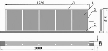
Module of the transformer stage is assembled from five blocks, connected in parallel. The module design is shown in Figure 2. The blocks (1) are placed on a basement (2) made from a steel channel and fixed to the plate (4) through the threaded rods (3). Ten contact plates (bronze), connected with HV capacitor terminals, are embedded in the plate (4). Low voltage terminals of the capacitors are in contact with the basement (2) in the same fashion. Charging voltage to the blocks is delivered through transition insulator in the last block. Transition insulators are also installed between blocks for transfer of the charging voltage from block to block. Wire resistor about 12 Ω is embedded in the insulator. This resistor limits current in the switch of the block in case of its self-breakdown. The high voltage wire surrounded by polyethylene insulation is passed consecutively through all electrodes with holes in all five blocks. Triggering pulse is applied from both sides of the module in order to reduce time delay in triggering between blocks. Module dimensions are given in Figure 2. Weight of the module is about 110 kg.
Assembly of the stage module: 1 is the capacitor block, 2 is the basement, 3 is the caprolon rods, 4 is the delta-wood plate.

2.3. Transformer Stage
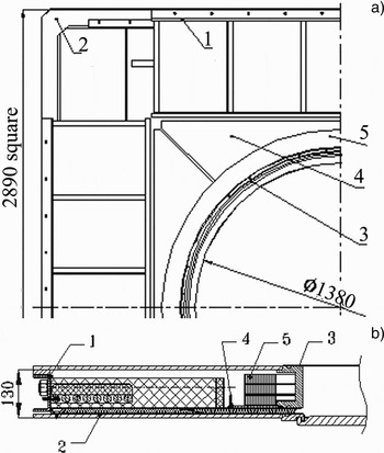
The transformer stage is assembled from four modules, connected in parallel on the LTD primary turn. The stage design is shown in Figure 3. The modules (1) are assembled on four sides of the basement plate (2) and fixed to it from the low voltage side. Acrylic insulator is placed between blocks of the modules and plate (2). Stage cores are placed on the combined electrodes (4) around the support ring (3). Combined electrodes (4) and the stage basement are fixed to this support ring (3). Stage dimensions are shown in Figure 3. Weight of the stage is about 1200 kg.
Transformer stage design: (a) top view of one quarter of the stage; (b) partial cross section through central axis. Here 1 is the module of the LTD stage, 2 is the basement plate, 3 is the support ring, 4 is the combined electrodes, 5 is the inductor core.

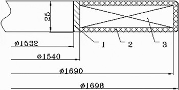
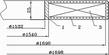
Inductor of the transformer stage (position 5, Fig. 3) consists of three cores. Each core is winded by a transformer steel strip of 18 mm width and 50 µm thickness, with insulating 10 µm Mylar tape between turns. The core is mounted on a holder from 5 mm thick steel with width of 25 mm. All three cores are mounted on the steel support ring (position 3, Fig. 3). The core sketch is shown in Figure 4. The length of the core middle line is about 4.78 m, total number of turns is about 1215, and weight of steel in the core is about 57 kg. Cross-section area of the inductor is about 33 cm2. Front and rear surfaces of the cores are filled in epoxy compound.
Design of the stage inductor: 1 is the holder, 2 is the epoxy compound, 3 is the core.
3. ELECTRICAL MODEL OF THE STAGE
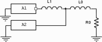
Equivalent electrical scheme of the stage, shown in Figure 5, was used for evaluation of the stage performance. Designations in the scheme are as follows: A1 is a two terminal network, substituting 20 capacitor blocks, connected in parallel; A2 is a two terminal network, substituting the stage inductor core; L1 is an equivalent inductance of a transmission line between capacitor blocks and cylindrical conductor with diameter of 1380 mm; L0 is an inductance of the stage load, which is placed inside the conductor with diameter of 1380 mm; R0 is a load resistance.
Equivalent electrical scheme of the stage.

3.1. Capacitor Blocks (A1)
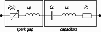
Equivalent scheme of a discharge circuit for one capacitor block is given in Figure 6. Here Cc = 80 nF and Rc ≈ 0.05 Ω are the block capacitance and active resistance, respectively. Lc ≈ 55 nH stands for equivalent inductance of one capacitor block in the stage. This value was derived from experiments with one capacitor block. R P(t) and L P are dynamic resistance and inductance of the multichannel switch.
Electrical scheme of the capacitor block. Here C C, L C, R C are the capacitors parameters; R P (t), LP is the electrical parameters of the switch.

Inductance L1 was estimated from the geometry of the transmission line between capacitor blocks and cylindrical conductor with diameter of 1380 mm that serves as outer conductor of the load chamber. It results in L1 ~ 1.4 nH. Load active resistance R0 is defined by a required discharge regime. Load inductance L0 was defined also from the geometry consideration. If active elements of the load equivalent are placed equidistantly on diameter of about 1324 mm, the load inductance is  .
3.1.1. Switch Model
Switch resistance Rs(t) and inductance Ls(t) were simulated with use of the Braginskii (Reference Braginskii1958) model, which implies hydrodynamic expansion of a spark channel in approximation of constant conductivity. According to this model, transition resistance of a spark gap is defined as:
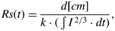
where d is the total inter-electrode gap in a switch, k is the constant, which depends on sort of working gas, pressure, and electrical conductivity of the channel. For air at atmospheric pressure, specific electrical conductivity is σ ~ 300 (Ωcm)−1, constant k ≈ 1.2 × 10⁵ (Andreev & Orlov, Reference Andreev and Orlov1966).
We consider that the switch inductance consists of two parts: constant Le is the inductance of the ball electrodes and dynamic L2(t) is the inductance of the expanding spark channel. The inductance of the ball electrodes is estimated by formula for one wire line with ground as current return at high frequency:

where l = 22 × 8 = 176 mm, r is the line radius, which is taken as half of the ball radius. Dynamic inductance of the spark channel is estimated by formula for one wire line with ground as current return, when distance to the ground is much more than line radius:

Channel radius r(t) is calculated according to the model:
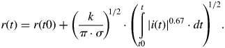
Initial radius channel (at beginning of a spark phase) is taken as r(t0) ~ 0.01 cm. Calculations reveal that channel inductance varies from about 145 nH to 120 nH during current pulse. Use of the average value Lch ~ 130 nH for inductance instead of dynamic inductance L(t) provides reasonably accurate approximation for calculation of the inductive voltage drop on the switch. In this case, inductance of switch with six channels would be Ls = Lch/6 = 21.7 nH.
3.2. Inductor Core (A2)
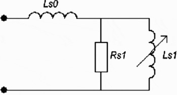
Equivalent scheme for the inductor modeling is given in Figure 7. Here Ls0 is the inductance part of the inductor contour with air gap; Rs1 and Ls1 are parameters of the ferromagnetic cores of the inductor. The cores are winded by transformer steel ET-3425 (saturation field Bs = 1.9 T, reset field Br = 1.4 T, electrical resistivity 0.5 × 10⁻⁶ Ωm).
Equivalent scheme for the inductor modeling.

Resistance Rs1 in the equivalent scheme provides energy loss in cores, corresponding to the experimental value. Inductance Ls0 is estimated from the inductor geometry. Inductance Ls1 is also estimated from the inductor geometry also taking into account relative magnetic permeability of the cores. Our simulation model implies that the relative magnetic permeability of the cores μ drops instantly from constant value μ1 to μ2 at a moment when volt-second integral reaches saturation value of about 11 mVs. Mean relative magnetic permeability of the multi-layered cores in saturated state is μ2 ~ 4–7. Value of Rs1 in the equivalent scheme (Fig. 7) and more accurate values for μ1, μ2 have been derived from our preliminary experiments with a stage prototype. Voltage and current in the inductor circuit have been measured in those experiments. Satisfactory agreement between calculated and experimental curves for voltage and current has been obtained at Rs1 ~ 0.9 Ω, μ1 ~ 300, μ2 ~ 4.
4. EXPERIMENTS WITH WORK OF A TRANSFORMER STAGE ON ACTIVE EQUIVALENT LOAD
Stages tests were performed with equivalent load that was assembled from 300 or 600 resistors (27 Ω each), connected in parallel. Load resistance in the first case is R = 0.1 Ω, L ~ 0.8 nH, in the second one is R = 0.05 Ω, L ~ 1 nH. The load was placed inside of the cylindrical chamber (diameter of 1380 mm). The load volume was filled by SF6 gas in order to prevent current losses from the load elements. The stage was tested in two regimes: (1) maximum output parameters of the stage were derived at opened circuit of the inductor, when all of the current flows through the load; (2) at connection of outer conductor of the stage coaxial (diameter of 1380 mm) with outer perimeter of the stage basement, the inductor circuit is connected in parallel with the load. This regime corresponds to the operation of the transformer stage, incorporated in a LTD assembly.
Load voltage was measured by an active voltage divider. Current derivatives (dI/dt) in the load and inductor circuits were measured by B-dots in the experiments. Probe signals were acquired by Tektronix TDS 3054 digital oscilloscope (500 MHz, 4 channels, 5 Gs/s on each channel). Load voltage and current derivatives were used for calculation of a load current, load power, load energy and energy loss, dissipated in the capacitor bank circuit.
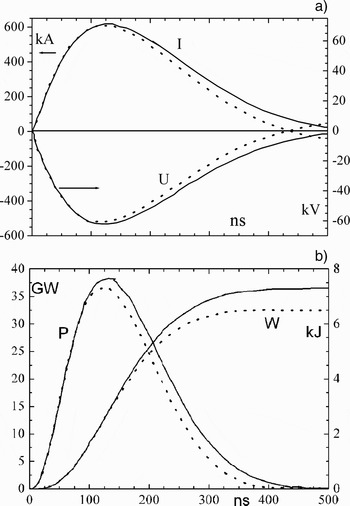
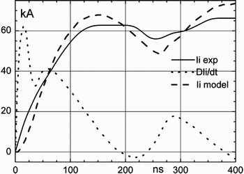
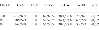
Inductor impact on the output pulse parameters was investigated with the 0.1 Ω load. Losses on the cores magnetization, current leakage in the inductor circuit, and volt-second integral were estimated in these experiments. Figure 8 shows experimental traces at charging voltage of 100 kV for regimes with opened and closed inductor circuit. In the first case, without leakage through the inductor circuit, amplitude of the load current is about 619 kA, current rise time up to maximum is about 130 ns, and amplitude of the load voltage is about 62 kV. The energy, delivered to the load, mounts to about 7.3 kJ from 8 kJ stored in the capacitors. Maximum load power is about 38 GW. At closed circuit of the inductor, the load power and energy decreased to ~36.5 GW and 6.6 kJ, respectively. The difference in load energy for two variants provides experimental estimation of energy losses in the inductor ~700 J. It is worth noting, that this estimation can be considered as the upper limit, because the difference was not taken into account in energy losses in the switches and other active elements of the stage circuit for two operation regimes. One can see from waveforms of the inductor current Ii and its derivative dIi/dt (Fig. 9) that saturation of the inductors occurs at time moment ~220 ns after the pulse beginning. Volt-second integral at this time is about 10–11 mVs. Obtained inductor parameters correspond to calculations, performed according to technique of Vizir et al. (Reference Vizir, Maksimenko, Manylov and Smorudov2004).
Experimental waveforms at U0 = 100 kV for the load of 0.1 Ω. (a) I, U is the load current and load voltage, (b) P is the load power, W is the load energy. Solid line is the opened inductor contour; dotted line is the closed inductor contour.

Ii experiment and Ii model are measured and calculated currents in the inductor circuit, dIi/dt is the derivative of the inductor current for 0.1 Ω load.

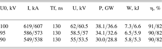
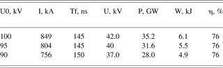
Results of investigations with 0.1 Ω loads are summarized in Table 1 for charging voltage of 90–100 kV and two operation regimes. The following notation is accepted in the table: U0 is the charging voltage of the stage; I is the amplitude of a load current; Tf is the rise time to the current maximum; U is the amplitude of the load voltage; P is the load power; W is the load energy; η is the efficiency of transfer of stored energy to the load.
Pulse parameters depending on charging voltage. Load 0.1 Ω, inductor circuit is opened/closed
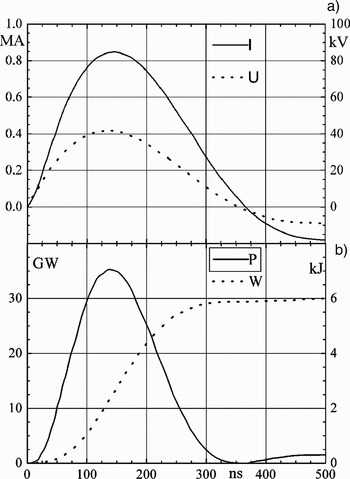
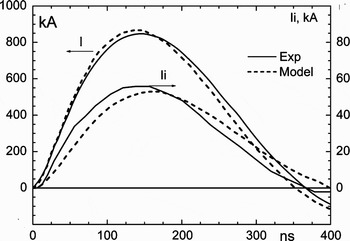
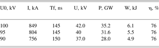
Decrease of a load resistance to 0.05 Ω results in increase of the stage current, but somewhat decreases output power and efficiency of transfer of stored energy to the load. For example, amplitude of the load current was about 850 kA at 100 kV charging voltage in regime with the closed inductor circuit, current rise time was about 145 ns. Load power and energy were about 35 GW and 6.1 kJ, respectively. The efficiency of transfer of stored energy to the load has been decreased from 82 to 76% in comparison with the stage operation on the 0.1 Ω load. Figure 10 shows waveforms for 0.05 Ω loads with closed inductor contour. Results of investigations with 0.05 Ω loads are summarized in Table 2 for charging voltage of 90–100 kV. Experimental and calculated waveforms for the load and inductor currents (0.05 Ω loads) are given in Figure 11. Comparison of experimental and calculated waveforms for inductor currents (0.1 Ω loads) is shown in Figure 9. One can see that accuracy of calculations is about 5%.
Experimental waveforms at U0 = 100 kV for the load of 0.05 Ω at closed inductor contour: (a) I, U – load current and load voltage, (b) P – load power, W– load energy.

Experimental and calculated waveforms of the load current (I) and current in the inductor circuit (Ii) for 0.05 Ω load.

Pulse parameters depending on charge voltage. Load 0.05 Ω, inductor circuit is closed
5. CONCLUSION
A new LTD stage has been developed with output power level of about 40 GW. Reliable and stable operation of the stage was demonstrated at charging voltage of up to 100 kV in air at atmospheric pressure. Comparison of the stage tests with tests of the single capacitor block proves synchronous and stable operation of connected in parallel capacitor blocks. Such a stage can be used as an element base at development of high power-pulsed generators with current ~106 A, voltage ~106 V without transformer oil and pressurized gas switches. Simulation model was developed for prediction of the spark gap performance. Reasonable agreement between experiment and simulation was obtained and it allows one to use this simulation technique for fast LTD generators development.