I. INTRODUCTION
Molecular electronics promises to deliver ultra high-density memory and logic circuits that can be realized with dimensions well below the scaling limits of conventional top-down fabrication methods associated with silicon technology. Reference Joachim, Gimzewski and Aviram1 Acquiring control over electronic transport at the atomic scale requires the ability to fabricate electronic devices in atomic resolution. The high level of control over the atomic structure of organic molecules promoted the use of molecular junctions (MJs) as a testbed for electronic transport at the atomic scale. Reference Nitzan and Ratner2–Reference Venkataraman, Klare, Tam, Nuckolls, Hybertsen and Steigerwald7 However, the structure of these junctions is limited to a molecule sandwiched between two macro-scale electrodes with typical conductance restricted to off-resonance tunneling (several orders of magnitude lower than G 0). Ideally, one would like to have the freedom to wire individual organic molecules to other atomic scale conductors Reference Yanson, Bollinger, Van den Brom, Agrait and Van Ruitenbeek8–Reference Smit, Untiedt, Yanson and van Ruitenbeek10 with minimal conductance attenuation to form efficient MJs based on more than a single atomic scale component junction. The wiring process while making MJs is done in a mechanically controllable break junction set up by pulling atom after atom from metallic electrodes. When atomic chains are pulled between metallic electrodes in the presence of diatomic molecules, the chains can be decorated by the small molecules or their decomposed atoms. Reference Csonka, Halbritter and Mihály11–Reference Wu, González, Huber, Grunder, Mayor, Schönenberger and Calame16 In the case of organic molecules connected by thiol groups between two gold electrodes, stretching the junction can lead to its elongation. Reference Xiao, Xu and Tao17–Reference Cheng, Skouta, Vazquez, Widawsky, Schneebeli, Chen, Hybertsen, Breslow and Venkataraman20 Direct binding of alkanes to gold electrodes showed similar behavior. Reference Dorogi, Gomez, Osifchin, Andres and Reifenberger21 A variety of MJs have been synthesized and experimentally studied Reference Andres, Datta, Dorogi, Gomez, Henderson, Janes, Kolagunta, Kubiak, Mahoney, Osifchin, Reifenberger, Samanta and Tian22–Reference Mujica, Kemp, Roitberg and Ratner36 by numerous researchers in an attempt to better understand their important conduction mechanisms. The intensity of this experimental activity has been equally matched by another group of researchers by increasing theoretical efforts. Reference Mujica, Kemp, Roitberg and Ratner36–Reference Emberly and Kirczenow45 The molecular wires in these junctions studied till date can be broadly divided into two categories. The first category is based on n-alkane chains which have large band gaps (approximately 6 eV or greater) between the highest occupied molecular orbital (HOMO) and the lowest unoccupied molecular orbital (LUMO) and are relatively insulating. Reference Di Ventra, Pantelides and Lang46 These molecules have flexible chains that pack well into dense, ordered monolayer films and are useful for forming insulating layers. The second category is based on conjugated polymers which have a small (2–4 eV) HOMO–LUMO gap (HLG) and behave much like ordinary semiconductors. Reference Durig, Zuger, Michel, Haussling and Ringsdorf47,Reference Reed, Randall, Aggarwal, Matyi, Moore and Wetsel48 These molecules are rigid and possess delocalized π-electrons, providing a relatively simple system to study and control. Such a metal–molecule–metal configuration would present the molecular embodiment of a system analogous to a quantum dot, Reference Meirav, Kastner and Wind49–Reference Tour, Jones, Pearson, Lamba, Burgin, Whitesides, Allara, Parikh and Atre58 with the potential barriers of the semiconductor system being replaced by any existing contact barrier of the molecule–metal interface. An important strategy in fabricating molecular electronic devices is preparing self-assembled monolayers (SAM) structures on an electrode and attaching a second electrode in such a way so as to form wires, diodes, switches, etc. Reference Toyoda, Morimoto and Morita59 The flexible nature of individual organic molecules and their rather unstable attachment to the electrodes can make the control of devices based on single molecules very difficult. On the other hand, intermolecular interactions within the SAM can possibly provide well defined molecular structures and correspondingly a more robust device control mechanism.
Calculations of molecular conduction must address the complexity of molecular motion and contact rearrangement under bias. H. Basch, R. Cohen, and M.A. Ratner in 2005 illustrated how different molecular orientations can change the calculated conductance up to order of thousand units. Reference Basch, Cohen and Ratner60,Reference Kaur, Sawhney and Engles61 Changes made in the electrode material of MJs can also lead to conductance variation up to a few percent and an order of magnitude. The electronic coupling between the metal and the molecule leading to partial or total Fermi-level pinning depends on the chemical reactivity of metals. Reference Xue and Ratner62 In some cases, if the metal chemically reacts with the end-group of the molecule (e.g., Au on thiol-terminated molecules), this overlayer may further prevent the diffusion of metal atoms into the organic monolayer. Reference Ke, Baranger and Yang63 The metal–organic interface interactions (e.g., interface dipole, charge transfer) are very critical and they have a strong impact on the electrical properties of the molecular devices. Reference Ke, Baranger and Yang64 If the metal atoms are not too reactive (e.g., Al with CH3 or OCH3), Reference Herdt and Czanderna65–Reference Konstadinidis, Zhang, Opila and Allara70 they can penetrate into the organic monolayer, diffusing to the bottom interface where they can eventually form an adlayer between this electrode and the monolayer (in addition to metallic filamentary short circuits). In this work, we have presented a computational approach addressing the charge transport properties of MJs by varying their atomic contacts. Changes in the electrical conductance of a single molecule as function of different material of atomic contacts were demonstrated.
II. MODELING AND COMPUTATIONAL METHODS
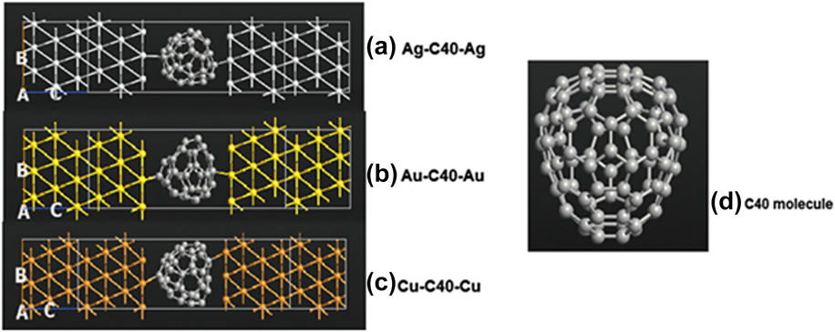
Our calculations are based on codes utilizing the nonequilibrium Green's function (NEGF) approach Reference Taylor, Brandbyge and Stokbro71 combined with ab initio density functional theory (DFT). Reference Lang72–Reference Taylor, Guo and Wang75 We have modeled three different MJs by sandwiching a quasi fullerene C40 molecule between two semiinfinite electrodes with varying metallic contacts Ag 〈1,1,1〉, Au 〈1,1,1〉, and Cu 〈1,1,1〉, as shown in Fig. 1. We deploy 〈1,1,1〉 electrode orientation as nanowires have strong likelihood along this direction. Reference Rodrigues, Fuhrer and Ugarte76 According to Reed et al., the approach of buffering a molecule or molecular wire between two metals presents the statically stable contacts and concurrently restricts the number of active molecules to as few as one. Reference Reed, Zhou, Muller, Burgin and Tour77
Schematic representation of jelium model comprising C40 molecule sandwiched between (a) silver, (b) gold, and (c) copper electrode atoms (d) isolated C40 molecule.

C60 has been widely worked upon fullerene, as it is unique and stable because all its pentagons are isolated by hexagons. This condition is acknowledged as the isolated pentagon rule (IPR), which makes fullerenes comparatively stable. Reference Kharlamov, Kharlamova, Bondarenki and Fomenko78 Fullerenes having less than 60 carbon atoms cannot endorse IPR and therefore become highly unstable Reference Leszczynski79 and C40 is one of the categories of quasi fullerenes. Reference Balasubramanian80–Reference Xiao, Lin, Chiu, Fu, Lai and Li82 Since very little work has been done till date to explore electrical properties of quasi fullerenes, thus we have focused on MJs comprising C40 and observed the change in electrical properties when it was bonded between three different coinage metals. So-formed MJs are modeled and simulated using Atomistic Tool Kit 13.8.0 (Ref. 83) and its graphical user interface Virtual Nano Lab. 83 Double-zeta polarized basis set 84 for all the atoms of C40 molecule and electrodes are used in the system to determine highly accurate results. The calculations are obtained by using generalized gradient approximation (GGA) exchange correlation functional described by Perdew–Burke–Ernzerhoff. Reference Perdew, Burke and Ernzerhof85
Calculations on transport properties in the coherent low bias regime have focused on the Landauer–Imry scheme of elastic scattering probability using NEGF. Calculating current is possible after self-consistently solving the NEGF and the electrostatic potential to get the electronic density matrix. Reference Landauer86 By modeling these MJs, we have explored different range of behaviors such as HOMO and LUMO mediated conduction on the calculated current–voltage (I–V) and conductance–voltage (G–V) characteristics as the bias voltage is varied from −2 V to +2 V. This bias range is limited to small values as the upper limit is determined by the oxidation of metal and the lower limit is set by the reductive desorption of C-40 layer from metal surface. Reference Chen and Tao87 Two parameters, namely the equilibrium Fermi energy of the molecule and the voltage division of the applied bias across the molecule and some parts of the electrodes, making it an ‘extended molecule,’ are crucial in determining the conductance spectrum. Reference Heurich, Cuevas, Wenzel and Schön88–Reference Beebe, Kim, Gadzuk, Frisbie and Kushmerick91 The same molecule can give rise to totally different conductance spectra due to the different details of molecular bonding to different substrates. When transmission probability is 100%, conductance comes out to be 77.5 µS, which is the most efficient electron transport via a single conduction channel. This result is accurate for monovalent metals such as Cu, Na, Au, and Ag which have only one conduction channel. Reference Chen and Tao87 The only condition for such a ballistic conductance is that the length of molecular wire should be less than the mean free path that an electron can travel without any collision. Now, if transmission probability is 100%, then what can be the reason for smaller conductance? Its answer lies in the fact that the measurement of conductance involves the contacts between the molecular wire and electrodes, which gives rise to conductance of smaller magnitude given by expression: C(V) = 2e 2/h. [T(E)/(1 − T(E))]. Since in this work, we considered a quasi fullerene molecule C40, which is a good conductor of electricity, thus when it is stringed between such monovalent metals, conductance as high as conductance quantum G0 can be achieved.
The current–voltage (I–V) relation can be understood within the context of the Landauer–Buttiker formalism Reference Landauer86 which relates the current I to the applied voltage V and the transmission probability T(E, V) of an electron having energy E expressed as:
 $$I\left( V \right) = 2{e \over h}\int_{{\mu _{\rm{L}}}}^{{\mu _{\rm{R}}}} {T\left( E \right)\left[ {f\left( {E - {\mu _{\rm{L}}}} \right) - f\left( {E - {\mu _{\rm{R}}}} \right)} \right]} {\rm{d}}E\quad {\rm{.}}$$
In Eq. (1), µL and µR are the electrochemical potentials of left and right metal contacts, respectively. T(E, V) is the transmission function which can be calculated from knowledge of the molecular energy levels and their coupling to metallic leads. In this study, the transmission was calculated using a similar procedure as Reference Heurich, Cuevas, Wenzel and Schön88
 $${T^k}\left( {E,V} \right) = Tr\left[ {\mathop {{\Gamma _1}}\nolimits^k \left( {E,V} \right)\mathop {{G_{\rm{M}}}}\nolimits^k \left( {E,V} \right)\mathop {{\Gamma _2}}\nolimits^k \left( {E,V} \right)\mathop {{G_{\rm{M}}}}\nolimits^{k'} \left( {E,V} \right)} \right]\quad {\rm{,}}$$
where Γ(E) is the coupling function that gives information about the quality of the contact between the molecule and the electrodes and G M(E,V) are the Green's function.
To the lowest order of approximation, it can be assumed that the molecular energy levels simply float up by an amount eV mol equal to the average electrostatic potential in the molecule. More conveniently, the molecular energy levels can be considered as a fixed reference and the substrate can float down by eV mol. It follows that the electrochemical potentials in the two contacts μL and μR can be approximated by Reference Lawson and Bauschlicher89 :
 $${\mu _{\rm{L}}} = {E_{\rm{F}}} - e{V_{{\rm{mol}}}} = {E_{\rm{F}}} - \eta eV\quad {\rm{,}}$$
 $${\mu _{\rm{R}}} = {E_{\rm{F}}} - eV + e{V_{{\rm{mol}}}} = {E_{\rm{F}}} + \left( {1 - \eta } \right)eV\quad .$$
In Eqs. (3) and (4), E F is the equilibrium Fermi energy, e is the electron charge and the factor η describes how the electrostatic potential difference V is divided between the two junctions: η = V mol/V. From prior scanning tunneling microscope measurements, Reference Heurich, Cuevas, Wenzel and Schön88–Reference Datta90 the two contacts can be adjusted to be nominally symmetric and the value for the factor η is close to 0.5. This parameter is a useful way to describe the potential profile especially for short molecules where the electric field inside the molecule seems to have a minimal effect on the electronic conductance spectrum.
The conductance C(V) can be obtained from the derivation of Eq. (1) given as Reference Landauer86 :
 $$C\left( V \right) = {{{\rm{d}}I} \over {{\rm{d}}V}} = e\left[ {\eta G\left( {{\mu _{\rm{L}}},V} \right) + \left( {1 - \eta } \right)G\left( {{\mu _{\rm{R}}},V} \right)} \right] + \int_{{\mu _{\rm{L}}}}^{{\mu _{\rm{R}}}} {{{{\rm{d}}G\left( {E{\rm{,}}V} \right)} \over {{\rm{d}}V}}} \quad {\rm{.}}$$
Equation (5) separates out the three contributions to the conductance spectrum with the first two terms representing a weighted average of the transmission function at E = µL and at E = µR, and the weighting depends on the voltage division factor η. The third term represents the ‘Stark effect’ due to the electric field inside the molecule. The effect of the voltage division factor is particularly striking, as explained previously. Reference Landauer86 The reason is that if η were zero (as is often assumed), then the electrochemical potential of the substrate, µL, would remain fixed with respect to the molecular levels. The molecule would then conduct strongly as the electrochemical potential in the tip, µR, approaches the LUMO (for positive substrate voltage) or the HOMO (for negative substrate voltage). This would lead to a strongly asymmetric C(V) characteristic with a band gap reflecting the HOMO–LUMO separation. But if η is assumed to be 0.5, a more symmetric G(V) is obtained since the molecule can conduct through the HOMO (if E F is closest to the HOMO) or the LUMO (if E F is closest to the HOMO) for both polarities.
III. RESULTS AND DISCUSSIONS
A. Quantum transport at zero bias
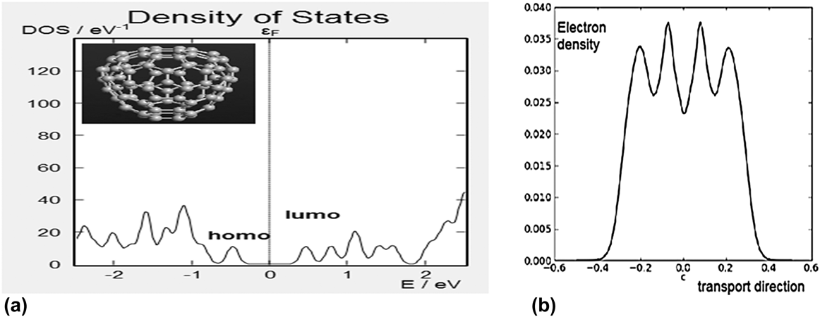
First, we discuss the molecular structure of an isolated quasi fullerene C40 molecule. C40 is a small cage fullerene molecule containing high pentagon/hexagon ratio, necessarily including adjacent pentagon pairs. Each carbon atom has three closest neighbors connected by single sigma bond and a delocalized pi bond. As the density of states (DOS) explains available quantum states in the vicinity of Fermi level for the molecule and device, band structure plots help in describing the conducting nature of electrodes in the bulk mode. The DOS and electron density of an isolated C40 molecule are calculated with DFT-GGA parameterization, as shown in Figs. 2(a) and 2(b) respectively. We clearly visualize a large number of peaks above and below E F. These peaks correspond to the available number of states that are used in transmissions. Peaks below E F exhibit high D(E) in contrast to those above E F, hence we predict the major contribution of HOMO mediated transmissions though C40. These molecular states experience shift in energies relative to E F, as the molecule is stringed between three different types of metal leads Ag, Au, and Cu as reported in Fig. 3. All the MJs experience HOMO mediated transmissions, since the resonance of strong HOMO peaks is located close to E F. Since MJ with Ag electrodes exhibit highest peak followed by Au electrodes and least by Cu electrodes, thus we firmly believe stronger conduction from Ag and Au electrodes in comparison with Cu electrodes at zero bias.
(a) DOS D(E) as a function of energy (eV) and (b) electron density as a function of transport direction of an isolated C-40 molecule.

Projected device DOS (PDDOS) of C40 molecule stringed between Ag, Au, and Cu electrodes.

Figure 2(b) reports the electron density of an isolated C40 molecule as a function of transport direction ‘c’ integrated over other two directions perpendicular to it, which are here ‘a’ and ‘b.’ The electron density of C40 molecule assays fluctuations from 0.023 to 0.038 units as the electrons drift across the transport direction of the molecule. This fluctuating electron density is directly analogous to the corresponding DOS [Fig. 2(a)] as these electrons populate the available states in D(E).
The transmission probability, according to Lorentzian formula, depends on two parameters: alignment of molecular orbital with metal Fermi level (E−E F) and broadening of the orbital due to hybridization with electrodes (τ). Both these parameters consider the Fermi level of metal electrodes, which further depends on chemical potential, thus making direct analogy of chemical potential of metal electrodes with the corresponding transmission probability given by Reference Kuwabara, Sugiyama, Yamaguchi and Takahashi93,Reference Paulsson and Datta94 :
 $$T\left( E \right) = {{{{\left( {{\tau \over 2}} \right)}^2}} \over {\left[ {{{\left( {E - {E_{\rm{F}}}} \right)}^2} + {{\left( {{\tau \over 2}} \right)}^2}} \right]}}\quad .$$
Beebe et al. Reference Beebe, Kim, Gadzuk, Frisbie and Kushmerick91,Reference Beebe, Kim, Frisbie and Kushmerick92 found the relation between potential barrier with the transmissions and conductance. The dependence of work function of the contacts on their resistance provides strong evidence of HOMO assisted tunneling and the system can be realized in terms of Schottky-like interfacial electronic barriers that result from energy level alignment. Reference Cukier and Cave95
To describe the conducting nature of electrodes, we compute the chemical potentials of the metals Cu, Ag, and Au as 4.73, 4.26, and 5.3 eV, respectively. Chemical potential establishes the relation between work function and the corresponding probability of transmissions through metallic substrate as described in Eq. (6). Thus, from the calculated values, Au exhibits highest work function while Ag shows lowest and Cu being intermediate. Thus, former requires larger potential energy (eV) for electrons to be added or knocked out of the system, while latter assay the requirement of lesser potential energy (eV) to overcome its band gap. Reference Paulsson and Datta94 PDDOS of MJs formed with Ag and Au electrodes are in agreement with the calculated values of chemical potentials. However, MJs with Cu electrodes contradict the same as its PDDOS spectra portrays lesser availability of DOS than that with Au due to small resonant peaks near E F, though Cu electrodes have smaller band gap than Au electrodes. Thus, it becomes imperative to explore the conducting behavior of so-formed MJs.
The distribution of the molecular orbitals and the extent of hybridization of central C40 molecule with different metal electrodes is obtained from the comparative analysis of PDDOS and transmission spectra at zero bias. The transmission probability T(E) as a function of energy is presented in Fig. 4. The necessary information about the participating molecular orbitals and their HLG is derived from the transmission spectra. Since the transmission coefficients T(E) are peaked around the molecular energy levels, it reflects the delocalized nature of chemical bond. It signifies the involvement of delocalized π-electron states of the carbon atoms of C40 molecule participating in charge transport phenomenon. The transmission spectra of all the MJs show clear correspondence with their PDDOS spectra. Figure 4 narrates the resonance of a sharp narrow HOMO peak positioned at −0.04 eV and approximately 0 eV for Ag–C40–Ag and Au–C40–Au MJs respectively, whereas broader HOMO resonance peak at −0.6 eV is reported by Cu–C40–Cu MJ. Meanwhile, broad LUMO peaks at 1.48 and 1.54 eV for Ag–C40–Ag and Au–C40–Au MJs, respectively, whereas smaller narrow LUMO peak at 0.12 eV dictates the dominance of conduction through HOMO energy level. Likewise, HLG of 1.52 eV and highest transmission coefficient at Fermi energy T(E F) for Ag–C40–Ag MJ reflects the strongest coupling of C40 with silver electrodes at zero bias. Cu–C40–Cu MJ portrays least HLG of 0.72 eV, but its smaller transmission probability at E F signifies weaker coupling of C40 with copper electrodes. Besides, intermediate HLG of 1.54 eV and T(E F) of 1.753 assay intermediate coupling strength between C40 and gold electrodes. The perfect alignment between energy levels of C40 with silver and gold electrodes and thus their higher conductance is perceived. However, the molecular states of C40 molecule failed to align perfectly with copper electrodes, hence exhibiting weaker conduction. The conducting trends of 1.8, 1.7, and 1.4G 0 are explicitly calculated for Ag–C40–Ag, Au–C40–Au, and Cu–C40–Cu MJs, respectively, at equilibrium. Thus, we successfully establish the relation between the position and strength of transmission coefficients of the participating orbitals with their corresponding conductance.
Equilibrium transmission spectra exhibited by three MJs.

To explore the origin of these transmission peaks at zero bias, their corresponding study of molecular projected self-consistent Hamiltonian (MPSH) eigen states Reference Kaur, Sawhney and Engles96 is done, which is discussed below.
From the full Hamiltonian H and overlap matrix S of the MJs, we projected onto the subspace spanned by the basis functions of the molecule C40 (Ref. Reference Chen and Tao87):
 $${H_{{\rm{mol}}}} = {P_{{\rm{mol}}}}H{P_{{\rm{mol}}}}\quad ,$$
where P mol is a projection matrix with unit diagonal elements on the indices of the molecule basis functions and zeroes elsewhere. Similarly, we computed a molecule overlap matrix S mol and the eigen value problem can be solved as:
 $${h_{{\rm{mol}}}}{C_n} = {€_n}{S_{{\rm{mol}}}}{C_n}\quad .$$
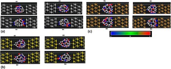
The eigen energies are calculated relative to electrode E F (0 eV) and included charge transfer effects between C40 molecule and metal electrodes, shown in Fig. 5.
Eigen states of C40 molecule of three junctions (a) Ag–C40–Ag, (b) Au–C40–Au, and (c) Cu–C40–Cu, where red and blue color denoted different orbital phases.

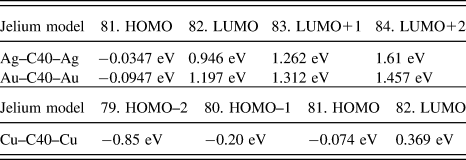
Figure 5 and Table I show the frontier orbitals relevant for transmissions around E F. It is evident that smaller HOMO peaks near E F with −0.04 eV and approximately 0 eV in the transmission spectra of silver and gold MJs are due to the participation of orbital number 81 with energy −0.0347 and −0.0947 eV, respectively. Since these states have vanishing orbital weight close to Ag and Au electrodes, the broadening due to these electrodes is fragile, resulting in narrow transmission peaks. Reference Perdew, Burke and Ernzerhof85 On the other hand, the broad transmission peaks at 1.48 and 1.54 eV for Ag and Au electrodes are associated with three eigen states LUMO (orbital number 82), LUMO+1 (orbital number 83) and LUMO+2 (orbital number 84) as reported in Table I. MJ with Cu electrodes exhibits different eigen characteristics with broader HOMO transmission peak and narrow LUMO peak. The broad HOMO transmission peak at −0.6 eV below E F is due to three eigen states HOMO−2 (orbital number 79), HOMO−1 (orbital number 80), and HOMO (orbital number 81), −0.85, −0.20, and −0.074 eV whereas narrow LUMO peak at 0.12 eV above E F is because of the vanishing orbital weight of LUMO (orbital number 82) at 0.369 eV due to which the coupling of C40 and Cu electrodes is weakest and hence assay narrow LUMO peak, portrayed in Fig. 5. Thus, very strong transmission peaks near E F in Ag and Au MJs contribute to high conductance of 1.8 and 1.71 times quantum conductance whereas allusive meager transmission peaks in MJs with Cu electrodes result in comparatively lesser conductance of 1.42 times quantum conductance at zero bias. Hence, at zero bias, Ag–C40–Ag is concluded to be highly conductive followed by Au–C40–Au MJ whereas Cu–C40–Cu least conductive though the nature of conduction predicted from chemical potential trends differ for copper and gold electrodes.
MPSH orbital numbers and their corresponding orbital energy relative to E F taken as 0 eV.

B. Quantum transport during finite bias
On the application of variegated bias from −2 to +2 V across three testbeds, their quantum transport under finite bias is discussed in this section of paper. As the finite electrochemical potential represented as parameter µi (i = L, left electrode or R, right electrode) is applied across the MJ, the system is driven out of equilibrium. Our elementary investigation starts with the resonant transmission channels accounting for the flow of charge through jelium model.
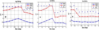
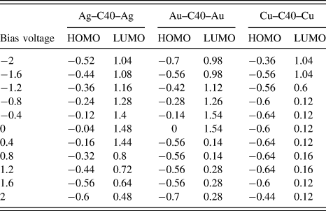
Under the influence of bias voltage, the potential profile across the molecule varies, which results in shifting of energy levels toward or away from Fermi level. So, we compute the energy levels of resonant HOMO and LUMO eigen states by analyzing their transmission spectra at different bias voltages. The variation of energy levels with the variegating bias voltage is shown in Fig. 6 and Table II. This asymmetric shifting of molecular orbitals results in the modulation of nature of coupling between C40 and metallic leads. This energy shift of the contributing molecular orbitals can be expressed as Eq. (9) (Ref. Reference Kaur, Sawhney and Engles96)
 $$\Upsilon = {{{f_{\rm{S}}} - {f_{\rm{T}}}} \over {2{f_{\rm{S}}} + {f_{\rm{T}}}}}\quad ,$$
where
 $\Upsilon$
is the molecular orbital energy and ſS,T represents the molecule–electrode coupling. The bias-driven asymmetric shift of the molecular orbitals can be related to the molecular electrode couplings with a parameter Ơ that quantifies this asymmetry as:
 $$\Upsilon = {{1 - {\rm{Ơ}}} \over 2}\quad .$$
Shifting of molecular orbitals HOMO and LUMO and hence HLG as a function of bias voltage for three testbeds under study.

Molecular orbital energies (eV) as a function of bias voltage.

Both the molecular orbitals HOMO and LUMO of MJs with gold electrodes exhibit prominent shift of energies during different bias voltages, as observed in Fig. 6. On the other hand, MJs made of copper electrodes experience least shifting of molecular orbitals, whereas junction with silver electrodes displays intermediate delocalization of HOMO and LUMO. Moreover, HOMO levels of both Ag–C40–Ag and Au–C40–Au MJs assay shifting of energy toward Fermi level as the bias is varied from −2 to 0 V followed by shifting away from Fermi level as the bias is further increased to +2 V.
However, LUMO levels exhibit reverse shifts i.e., they shift away from Fermi level with change in bias voltage from −2 to 0 V followed by energy shifts toward Fermi level as the bias voltage is increased to +2 V. Thus, both the energy levels contribute equally in the conduction as HOMO participates during reverse bias whereas LUMO participates during forward bias. However, least delocalization of HOMO level is witnessed in Cu–C40–Cu MJ illustrating the proximate presence of LUMO orbital relative to E F. As the resonant HOMO levels of both Ag–C40–Ag and Au–C40–Au MJs are peaked close to E F, thus quantum transport in both these MJs is feasible through HOMO conducting channel.
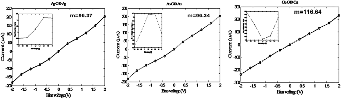
From the transmission coefficients computed through transmission spectra at different energies for different values of bias voltage, we compute the values of current and conductance by using Eqs. (1) and (5). Based on an ample volume of literature on electron transfer in the molecular systems, dominant current transport mechanism in MJs is found to be ‘through-bond tunneling’ Reference Bâldea97 in which current follows the bond overlap across the molecule C40 rather than ‘through-space tunneling.’ Current spectrum I(V) shown in Fig. 7 assays metallic nature since all the I–V curves exhibit similar linear characteristics with Ag–C40–Ag, Au–C40–Au, and Cu–C40–Cu MJs having slopes of 96.37, 96.34, and 116.64, respectively. Silver and gold electrodes exhibit minor nonlinearity at high bias voltage points ±1.2 V and thus illustrate rectification mechanism.
Current spectrum I(V) exhibited by three different MJs in which all of them assayed metallic behavior. Inset shown is their varying trends in RRs.

MJs exhibit differing rectification ratio (RR) trends shown in inset of Fig. 7. Asymmetric evolution of molecular orbitals under reverse and forward bias from −2 to +2 V gives rise to different strengths of current at different bias voltages and hence, rectification. Reference Chen and Tao87 As discussed above, Au–C40–Au MJ experiences maximum orbital delocalization with the variation in bias voltage, which accounts for maximum change in the magnitude of current. Large variation in the magnitudes of current at ±V gives rise to high RR as seen in MJ formed with gold and silver whereas small difference in the values of currents at ±V result in small RR as in case of Cu–C40–Cu. Au–C40–Au and Ag–C40–Ag portray maximum RR of 1.2 and 1.12, respectively, at ±1.6 V whereas Cu–C40–Cu exhibits maximum RR of 0.98 at ±0.4 V. From Table II, at −1.6 V, we observe the HOMO and LUMO energies of Ag–C40–Ag MJ peaked at −0.44 and 1.08 eV which shift to −0.56 and 0.64 eV, respectively. HOMO orbital exhibits shift away from Fermi level by 0.12 eV whereas LUMO shifts toward Fermi level by 0.44 eV. This prominent shift of LUMO toward Fermi level accompanied by minor shift of HOMO away from Fermi level escalates the strength of current from −133.92 to +150.09 µA, giving rise to RR = 1.12. Similarly, energy shift of 0.7 orders of LUMO from 0.98 to 0.28 eV and localized HOMO at −0.56 eV results in change of the magnitude of current from −130.79 to +159.37 µA accounting for RR = 1.2. Since no delocalization of HOMO and LUMO orbitals is assayed by Cu–C40–Cu MJ, it exhibits negligible RR of 0.98. Thus, localization and delocalization of HOMO and LUMO orbital energies at different bias voltage accounts for different magnitudes of current and thus RR. A team of Columbia Engineering researchers led by an Indian-American scientist Latha Venkataraman successfully created a single-molecule diode in 2015 (Ref. Reference Capozzi, Xia, Adak, Dell, Liu, Taylor, Neaton, Campos and Venkataraman98) which can perform 50 times better than all prior designs. This idea of using functionalized molecular circuit as a molecular diode was suggested by Arieh Aviram and Mark Ratner in 1974. Reference Aviram and Ratner99 Various researchers are now focusing their entire attention to increase the RRs of such diodes. Thus, by escalating RR, we can implement such single-molecule electronic devices for real-world technological applications at nanoscale.
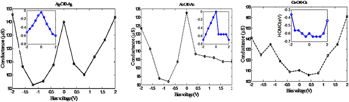
Further, the conductance spectrum G(V) is plotted as a function of bias voltage shown in Fig. 8. As portrayed in current spectrum, conductance spectrum also displays similar conductance trends exhibited by MJs formed by gold and silver electrodes. Conductance curves of all the MJs exhibit oscillations with the increase in bias voltage accompanied by highest conductance peak at zero bias for both Ag–C40–Ag and Au–C40–Au MJs.
Conductance spectrum G(V) displayed by MJs in which gold and silver contacts exhibited similarity in their conducting characteristics, inset shown is their HOMO orbital energy as a function of bias voltage.

This highest zero bias conductance peak is of order K B T K/e and calculated as 1.8 and 1.71G 0 by MJs with silver and gold electrodes, respectively. It reports lifting of coulomb blockade due to accumulation of large number of charge carriers at zero bias, shown in Fig. 9 and eventually Kondo assisted tunneling Reference Kaur, Sawhney and Engles100 on account of equal coupling of C40 to both metallic leads. It is a crossover from weak to strong coupling regime between localized orbitals and conduction band electrons of silver and gold electrodes, which manifest maximum conduction peak at zero bias. Reference Galperin, Nitzan and Ratner101 T. Tada and co-workers Reference Tada, Nozaki, Kondo, Hamayama and Yoshizawa102 attribute the conductance oscillation in a molecular wire to oscillatory behavior of electron populations of the frontier orbitals. Thus, in inset, we have plotted the orbital energies of HOMO as a function of bias voltage where Cu–C40–Cu MJs display exactly same oscillating trends in conductance spectrum as seen in the ripples elucidated by shifting HOMO energies with changing bias voltage. When HOMO is raised to E F, electrons transfer from C-40 molecule to one of the two electrodes and the molecule is said to be in oxidized state. However, as its energy shifts below E F, HLG and injection gap increases and molecule C-40 is said to be in reduced state. Thus, molecule can be switched from reduced state (low conductance) to oxidized state (high conductance) by tuning its external bias. Reference Chen and Tao87 Hence, MJ formed of copper electrodes exhibits strong correlation of its conductance with the delocalization of HOMO orbital, though its injection gap i.e., E F−E HOMO is comparatively larger than that of LUMO orbital i.e., E LUMO−E F. However, such a strong correlation in Ag–C40–Ag and Au–C40–Au MJs is not visualized. Thus, their G(V) curves are the resultant contribution of both HOMO and LUMO and their HLG and not on the delocalization of single orbital HOMO or LUMO. From the variations in HLG shown in Fig. 6, we observe decreasing HLG as the bias direction is varied from reverse bias to forward bias. Thus, strong metallic behavior exhibited by I–V curves of MJs is attributed to this fall in HLG and injection gap.
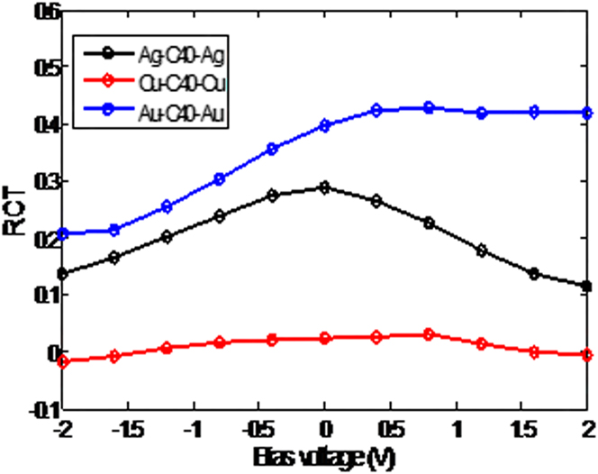
RCT as a function of bias voltage.

The electron charging energy describes the net energy change due to addition or subtraction of electrons from the molecule in the gap, Reference Tada, Nozaki, Kondo, Hamayama and Yoshizawa102 which broadens the molecular orbital conduction peaks, we have estimated this charge through charging energy ‘U’ expressed as Reference Andrews, Cohen, Van Duyne and Ratner103 :
 $$U = {{{\rm{EA}} - {\rm{IP}}} \over 2} - {{{E_{\rm{g}}}} \over {\rm{2}}}\quad ,$$
where EA is the electron affinity, IP is the ionization potential and E g expresses the vertical optical energy. Reference Tian, Datta, Hong, Reifenberger, Henderson and Kubia104,Reference Ohno, Chen, Harvey, Kroll, Weaver, Haufler and Smalley105
So, we compute the Mulliken charge as a function of bias voltage on the central molecule C40 bound between three MJs and plotted in Fig. 9. With the tuning of external bias, we examine the changing relative charge transfer (RCT) on C40 quasi fullerene. MJ with Au electrodes assays maximum RCT throughout the entire bias followed by MJ with silver electrodes. Though, Au–C40–Au MJ exhibits maximum RCT, it could not contribute to maximum conductance because of higher work function of gold as reported in the beginning of this paper, due to which tunneling probability of electrons through C40–Au interface is not comparable with that of C40–Ag interface which exhibits maximum G. Cu–C40–Cu MJ portrays least charge transfer and thus lesser conduction than Ag and Au MJs. Thus, we establish a strong dependence of conductance on RCT trends which are responsible for shifting of orbital energies with the variation in bias voltage.
IV. CONCLUSIONS
In an effort to explore the effect of different metallic leads on the conductance of jelium model, we investigate the charge transport properties of C40 fullerene based MJs formed by different coinage metals copper, silver, and gold. The DOS, transmission spectrum, molecular orbital analysis, current, conductance spectrum and RR are computed using DFT-NEGF computational approach. The quantum transport at zero bias and finite bias are explored separately. We conclude our findings in following five points. First, all the MJs exhibit ballistic transport having conduction of 1.5 to 2 times of quantum conductance G 0. Second, RR results from asymmetric evolution of molecular orbitals at different bias with Au–C40–Au MJ assaying maximum RR of 1.2 and can make an efficient diode. Third, least HLG and perfect alignment of molecular orbitals with the E F of electrodes give rise to maximum conductance at zero bias for MJs formed with gold and silver electrodes while MJs with Cu electrodes illustrate this efficient hybridization at ±2 V. Fourth, all the MJs exhibit oscillatory conduction behavior on account of the comparable ripples observed in their varying orbital energies as a function of bias voltage. Fifth, MPSH analysis of the eigen states reveals the contribution of three orbitals for broad resonance peak and singlet state for narrow transmission peak near Fermi energy in transmission spectrum. We conclude very good agreement between current and conductance with their molecular orbital analysis, MPSH eigen states, and resonant eigen states, which are well described by DFT-GGA formalism used in this work.