I. INTRODUCTION
While electricity remains the most convenient form of energy in the foreseeable future, heat has been an abundant but low quality source of energy as more than half of all the energy generated by mankind is lost as waste heat. The simplest technology applicable for direct heat–electricity conversion is thermoelectricity.Reference Tritt, Subramanian, Bottner, Caillat, Chen, Funahashi, Ji, Kanatzidis, Koumoto, Nolas, Poon, Rao, Terasaki, Venkatasubramanian and Yang1 Heat emanating from various sources (e.g., solar, geothermal, and exhaust from automobiles or other industrial processes) can be directly converted into clean electricity by a thermoelectric (TE) device, which is an all-solid assembly without moving parts or greenhouse gas emissions, compact, responsive, and feasible for miniaturization. The TE device can also work reversely as a heat pump for refrigeration (heat management).
The conversion efficiency of a TE device is determined by the Carnot efficiency and the figure of merit, ZT, of the TE material.Reference Nolas, Sharp and Goldsmid2 Assuming a negligible contact resistance and optimized load condition, the maximum conversion efficiency of TE power generation, η, is expressed as

where the Carnot efficiency is given as the ratio of the temperature difference between the hot-end temperature and the cold-end temperature (T hot − T cold), to T hot, and T m is the mean temperature. ZT is the material parameter of prime importance in thermoelectrics research:

where α is the thermopower (or Seebeck coefficient), ρ the electrical resistivity, κ the thermal conductivity (κ l the lattice thermal conductivity and κ e the carrier thermal conductivity), PF the power factor, and T the temperature in Kelvin. Ideally, a TE material simultaneously possesses low ρ and low κ, i.e., a “phonon glass electron crystal” (PGEC) as coined by Slack,Reference Slack and Rowe3 along with a large |α|. Although there is no theoretical upper limit for ZT values, most state-of-the-art TE materials have a maximum ZT ∼1–2 in their respective temperature range of operation because of the interdependence of ρ, α, and κ. In the thermoelectrics community, ZT = 1 is regarded as a performance benchmark for viable TE materials.
Modern thermoelectrics research dates back to Ioffe’s observation in the 1950s that heavily doped semiconductors made the best TEs.Reference Ioffe4 The theory of semiconductor physics helps establish the basic principles of thermoelectricity and also imposes several guidelines on the bulk materials suitable for TEs. The first guideline states that the degenerate semiconductors or semimetals with carrier concentrations n∼1018–1020 cm−3 make good TEs because such n values maximize the PF. The second guideline states that the semiconductors with band gap Δ∼10 k BT o make good TEs,Reference Mahan5 where k B is the Boltzmann constant and T o the operating temperature. Such a band gap size ensures a reasonable value for the carrier mobility, μ, and minimizes the detrimental contribution from the minority carrier to α (i.e., the bipolar effect). GoldsmidReference Goldsmid6 pointed out that Z is determined by (m*)1.5μ, where m* is the effective mass of carrier. Enhancing m* without deteriorating μ leads to the third guideline: it is thermoelectrically favorable for materials to adopt a high-symmetry crystal structure (to have high band-degeneracy) and have small electronegativity difference among the constituent elements (to minimize the scattering of charge carriers by optical phonons). The fourth guideline concerns κ l: low κ l is often found in materials made up of heavy elements and/or with many atoms per unit cell. Most of the current state-of-the-art TE materials are in-line with these guidelines, they are degenerate semiconductor or semimetal bulk materials with high-symmetry crystal structure and contain one or more of the heavy elements Bi, Pb, Te, or Sb.
In view of these guidelines, however, oxides are believed to make poor TEs. First, the large electronegativity difference among the constituent elements leads to more ionic bonding, strong tendency for carrier localization, and strong scattering of carriers by optical phonons, the resulting μ may be orders of magnitude lower than that of the heavy element-based TE materials. Even for high mobility oxide semiconductors, |α| is often found to be small because of the cancellation between the electron and hole band contributions. Moreover, the large bonding energy and the small mass of oxygen lead to a high velocity of sound and, therefore, high κ l. This is why the good TE properties found in NaxCoO2 are peculiar and enlightening in pursuing novel mechanisms of thermoelectricity.Reference Terasaki, Sasago and Uchinokura7–Reference Fujita, Mochida and Nakamura9 Theoretical studies have suggested that the high α may be related to electron correlationReference Ando, Miyamoto, Segawa, Kawata and Terasaki10 and high carrier (spin and orbital) degeneracy,Reference Wang, Rogado, Cava and Ong11, Reference Koshibae, Tsutsui and Maekawa12 whereas Singh et al. argued that the high α can be explained by standard band theory on the basis of the splitting of t 2g manifold.Reference Singh and Kasinathan13
In this article, we present an overview of the recent progress of oxide thermoelectrics research. A comparison is made among the performance of several representative TE oxides in their different forms such as bulk material (single crystal and polycrystal), epitaxial film, and nanostructured material [two-dimensional (2D) electron gas system, superlattice, and nanocomposite]. In particular, the rationale, strategies, and experimental results of the emerging nanostructuring approach are highlighted. Finally, we briefly discuss the status of the TE oxide module development. Readers further interested in oxide thermoelectrics research are referred to excellent reviews by Koumoto et al.,Reference Koumoto, Wang, Zhang, Kosuga and Funahashi14 Ohtaki,Reference Ohtaki15 and Ohta et al.Reference Ohta, Sugiura and Koumoto16
II. OXIDE TEs
A. Merits of oxides
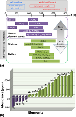
Although ZT of oxides is still low compared with the current state-of-the-art TE materials,Reference Vineis, Shakouri, Marjumdar and Kanatzidis17–Reference Minnich, Dresselhaus, Ren and Chen19 oxides possess several inherent merits from fundamental and application points of view. First, the high chemical and thermal stability of oxides allows for a large temperature gradient to be applied across the materials in air [Fig. 1(a)], thereby leading to a high Carnot efficiency in Eq. (1) that somewhat compensates the low ZT. Second, the large temperature gradient may induce novel nonlinear, nonlocal TE effects (e.g., the Benedicks effectReference Mahan20) that may be thermoelectrically favorable.Reference Anatychuk, Bulat and Rowe21 Third, oxides are featured by their chemical versatility and structural intricacy, which offering a great flexibility of structural and compositional tailoring. Finally, oxides are decidedly advantageous in terms of the cost of raw materials and the environmental friendliness. For any large-scale application of thermoelectricity, the cost of raw material is a major consideration after performance. For example, the increasing price of Te somewhat vitiates the enhancement of ZT in the Te-containing high-performance nanostructured TE materials.Reference Vineis, Shakouri, Marjumdar and Kanatzidis17–Reference Minnich, Dresselhaus, Ren and Chen19 Hence, high-performance TE materials based on abundantly available [Fig. 1(b)] and nontoxic elements with high chemical and thermal stability are crucial for any viable large-scale applications.Reference Vaqueiro and Powell22 As shown in Fig. 1(a), oxides are particularly suitable for high temperature power generation in air.
(a) Schematic comparison of various thermoelectric (TE) materials for applications of waste heat harvest and refrigeration, in terms of the temperature range of operation and the abundance and environmental friendliness of constituent elements. (b) The abundance of elements used in TE materials, the elements represented by dark-colored columns are <1 ppm.

B. “Hybrid crystal”
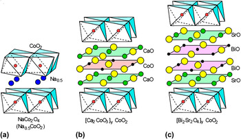
Since the discovery of the good p-type material NaxCoO2, a number of cobaltites with hexagonal CoO2 sheets that are structurally similar to those in NaxCoO2 have been prepared and studied from the TE perspective. Promising p-type TE properties have been found in Ca3Co4O9Reference Li, Funahashi, Matsubara, Ueno and Yamada23–Reference Nong, Liu and Ohtaki28 and Bi2Sr2Co2O9.Reference Funahashi, Matsubara and Sodeoka29–Reference Shen, Liu, Zhu and Zhao32 Studies on these layered cobaltite oxides have drawn on the important concept of the “hybrid crystal”Reference Koumoto, Terasaki and Funahashi33 in-line with the concepts of PGEC.Reference Slack and Rowe3 The basic idea of the “hybrid crystal” is that a complex crystal structure can be regarded as being formed by building modules with different compositions, structural symmetries, and, therefore, specific TE functions, the electrical and thermal transport can be thus somewhat decoupled and individually tuned to attain a higher ZT. As shown in Fig. 2(a), NaxCo2O4 adopts a hexagonal-layered structure with edge-sharing 2D triangle CoO2 sheets (“electron crystal”) and highly disordered Na layers (“phonon glass”) alternately stacked along c-axis. In Ca3Co4O9 and Bi2Sr2Co2O9, there is a lattice misfit between the hexagonal CoO2 sheet and the square Ca2CoO3 and Bi2Sr2O4 substructures [Figs. 2(b) and 2(c)].
Schematic crystal structures of the layered cobaltites (a) NaxCoO2, (b) Ca3Co4O9, and (c) BiSrCoO. (From Ref. Reference Koumoto, Terasaki and Funahashi33. Copyright Materials Research Society, reproduced with permission.)

Another example of a “hybrid crystal” is the Ruddlesden–Popper homologous series of Srm+1TimO3m+1 in which two basic building modules, SrO and SrTiO3, are alternately stacked. Promising n-type TE properties have been found in perovskite compounds with a general formula ABO3 (Srm+1TimO3m+1 with m =∞).Reference Ohta, Nomura, Ohta and Koumoto34–Reference Cui, He, Amow and Kleinke36 For example, heavily Nd-doped SrTiO3 (n∼1021 cm−3) exhibits a large PF of 3.6 × 10⁻³ W·m−1·K−2 at room temperature because of the large density of states (DOS).Reference Okuda, Nakanishi, Miyasaka and Tokura37 In particular, ZT of doped CaMnO3 has been significantly improved since 2008.Reference Kosuga, Isse, Wang, Koumoto and Funahashi38–Reference Huang, Miyazaki and Kajitani41
C. Other bulk oxides
In addition to the aforementioned layered structured cobaltites and ABO3 perovskites, many other bulk oxides have been studied from the TE perspective, to name a few, [(Bi,Pb)2Ba2O4±ω]0.5CoO2,Reference Sakai, Karppinen, Chen, Liu, Sugihara and Yamauchi42 Bi0.78Sr0.4RhO3+δ,Reference Kobayashi, Hébert, Pelloquin, Pérez and Maignan43 La0.95Sr0.05CoO3,Reference Androulakis, Migiakis and Giapintzakis44 La1-xSrxCrO3,Reference Weber, Griffin and Bates45 CuRh1xMgxO2,Reference Kuriyama, Nohara, Sasagawa, Takubo, Mizokawa, Kimura and Takagi46 doped In2O3,Reference Guilmeau, Bérardan, Simon, Gaignan, Raveau, Ovono Ovono and Delorme47 Ln (rare earth)-doped SrO(SrTiO3)n,Reference Wang, Lee, Ohta and Koumoto48, Reference Wang, Lee, Ohta and Koumoto49, Reference Lee, Wang, Hyuga, Kita, Ohta and Koumoto50 Li- and Na-doped NiO,Reference Shin and Murayama51 SrxCoO2 (x∼0.35),Reference Ishikawa, Ono, Miyazaki and Kajitani52 doped ZnO,Reference Ohtaki, Tsubota, Eguchi and Arai53–Reference Ohtaki, Araki and Yamamoto56 and In2O3(ZnO)m (m = integer).Reference Ohta, Seo and Koumoto57 Despite a wide variety of structures and compositions, these materials can be roughly grouped depending on their μ values. In contrast to In2O3 and ZnO with high μ values, the electrical conduction in doped La(Co,Cr)O3 is due to small polaron hopping,Reference Koc and Anderson58 featured by μ values much lower than the band conduction and a thermal activation type behavior of ρ. Interestingly, instead of a nearly temperature-independent α as expected from a small polaron system, La(Co,Cr)O3 exhibits a linear temperature dependence in α, reminiscent of the heterosite hopping in boron carbides.Reference Wood and Emin:59 In La(Co,Cr)O3 the large difference in the spin and orbital configurations of different valence states of Co/Cr cations give rise to a large carrier degeneracy and, therefore, high α.Reference Koshibae, Tsutsui and Maekawa12
D. Epitaxial films
The intrinsic TE properties of oxides are often difficult to determine because most of the as-synthesized oxides are in the form of small single crystals or polycrystalline ceramics. The growth of single crystals is time-consuming and expensive, whereas polycrystals usually have poorly characterized texture, grain boundaries, pores, and crystal chemistry (e.g., oxygen off-stoichiometry). Therefore, high-quality epitaxial films of several TE oxides, such as NaxCoO2,Reference Ohta, Mizutani, Sugiura, Hirano, Hosono and Koumoto60 Ca3Co4O9,Reference Sugiura, Ohta, Nomura, Hirano, Hosono and Koumoto61, Reference Sugiura, Ohta, Nomura, Saito, Ikuhara, Hirano, Hosono and Koumoto62 SrTiO3:Nb,Reference Ohta, Nomura, Ohta, Hirano, Hosono and Koumoto63 TiO2:Nb,Reference Kurita, Ohta, Sugiura, Ohta and Koumoto64 and SrO(SrTiO3)n:Nb (n = 1, 2),Reference Lee, Ishizaki, Kim, Ohta and Koumoto65 have been fabricated. In particular, a reactive solid phase epitaxy techniqueReference Ohta, Nomura, Orita, Hirano, Ueda, Suzuki, Ikuhara and Hosono66 has been developed to grow epitaxial films of p-type layered oxides containing high volatile elements. The high-quality epitaxial film is thermoelectrically favorable in that the thin film largely possesses the intrinsic electrical properties of the bulk single crystal and a lower κ because of strong phonon scatterings at boundaries. Transport properties measurements performed on these thin film samples suggest that some of the previously reported ZT values are questionable.Reference Ohta, Sugiura and Koumoto16
It is also found that NaxCoO2 decomposes into insulating Co(OH)2 in a high humidity environment because the Na+ ions easily dissolve in H2O, whereas Ca3Co4O9 exhibits good p-type TE properties and good thermal stability at 1000 K in air. The ZT of epitaxial film Ca3Co4O9 reaches ∼0.3 at 1000 K,Reference Ohta, Sugiura and Koumoto16 which is lower than that of p-type Si–Ge (ZT∼0.8).Reference Dismukes, Ekstrom, Steigmeier, Kudman and Beers67 The chances of further improving the ZT of Ca3Co4O9 may lie in enhancing |α| via optimizing the misfit ratio.Reference Ishiwata, Terasaki, Kusano and Takano68
E. Two-dimensional electron gas systems and superlattices
As for the n-type films, the ZT of epitaxial film SrTi0.8Nb0.2O3 reaches ∼0.3 at 1000 K.Reference Ohta, Sugiura and Koumoto16 However, further improving the ZT of ABO3 perovskites via a traditional doping approach has proved to be difficult.Reference Kato, Yamamoto, Ohta, Muta, Kurosaki, Yamanaka, Iwasaki, Ohta and Koumoto69–Reference Yamamoto, Ohta and Koumoto71 Hence, a novel technical route, i.e., 2D electron gas (2DEG), has been adopted to improve ZT via enhancing α. In general, |α| is a measure of the energy dependence of the DOS at the Fermi level (EF). The DOS(EF) of transition metal oxides (TMOs) is predominated by heavy d-electrons, therefore, the conduction electrons are expected to be localized more strongly in TMOs than in heavy element-based TE materials. In addition, quantum size effects (quantum confinement) are expected to further enhance the DOS(EF) in a 2DEG system. Ohta et al. have fabricated a superlattice system composed of insulating SrTiO3 (undoped, carrier concentration: n < 1015 cm−3) and highly conductive Nb-doped SrTiO3 (SrTi0.8Nb0.2O3, n = 2.4 × 1021 cm−3) on the (001)-face of LaAlO3 single crystal substrates by pulse laser deposition (PLD).Reference Ohta, Kim, Mune, Mizoguchi, Nomura, Ohta, Nomura, Nakanishi, Ikuhara, Hirano, Hosono and Koumoto72, Reference Mune, Ohta, Koumoto, Mizoguchi and Ikuhara73, Reference Lee, Mune, Ohta and Koumoto74 The room temperature α value is enhanced by a factor of about 5 (from −198 μV/K for bulk SrTiO3 to ∼−1000 μV/K for the 2DEG system) without deteriorating σ. Assuming the κ value of the bulk single crystal, the room temperature ZT is ∼2.4 for the 2DEG system, corresponding to a ZT∼0.24 for a complete device containing 2DEG as the active region. Figure 3Reference Ohta, Sugiura and Koumoto16 shows the Cs-corrected high-angle annular dark-field scanning transmission electron microscope image of an as-prepared superlattice system. The results of Ti-L2,3 edge electron energy loss spectroscopy show that the Ti column in one unit cell thickness of SrTi0.8Nb0.2O3 had a higher intensity than that of the SrTiO3 barrier layer, confirming that the doped Nb5+ ions are exclusively confined in the SrTi0.8Nb0.2O3 layer.
High-angle annular dark-field scanning transmission electron microscope image and Ti-L2,3 edge electron energy loss spectroscopy profile. (From Ref. Reference Ohta, Sugiura and Koumoto16. Copyright American Chemical Society, reproduced with permission.)

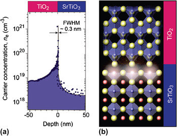
Another important 2DEG system has been fabricated at the heterointerface between oxygen-deficient TiO2-δ and SrTiO3. The TiO2-δ film possibly extracts O2– from the SrTiO3 substrate, introducing conduction electrons confined at the heterointerface between TiO2 and SrTiO3. Figure 4Reference Ohta, Sugiura and Koumoto16 shows the depth profile for the TiO2/SrTiO3 heterointerface. The full width at half maximum of the carrier concentration peak at the heterointerface is ∼0.3 nm, which is close to the lattice parameter of SrTiO3 (a = 0.3905 nm). Hence, a high concentration of conduction electrons is localized within a unit cell thickness of SrTiO3 at the heterointerface.
(a) Depth profile across the heterointerface between a TiO2 epitaxial layer and the SrTiO3 substrate. (b) Schematic drawing of the heterointerface crystal structure. (From Ref. Reference Ohta, Sugiura and Koumoto16. Copyright American Chemical Society, reproduced with permission.)

Both SrTiO3 and TiO2 have the TiO6 octahedra as the basic structural module. The shape of TiO6 octahedra in SrTiO3 is regular, and the Ti 3d-t 2g orbitals of 3dxy, 3dyz, and 3dzx are degenerate; the shape of TiO6 octahedra in TiO2 is irregular, and the 3dxy orbital has lower energy level compared with 3dyz and 3dzx because of the crystal field splitting.Reference Daude, Gout and Jouanin75 The comparison of carrier generation, transport properties, such as n, m*, and carrier relaxation time between SrTiO3 and TiO2 is thus instructive for future selection and design of titanate-based TE oxides. Kurita et al.Reference Kurita, Ohta, Sugiura, Ohta and Koumoto64 have proposed that the titanates with a high-symmetry structure would exhibit better TE performance than the low symmetry one, which is consistent with the third guideline discussed in the Introduction.
To reduce the production cost and to scale up the size of 2DEG systems, Ohta et al.Reference Ohta, Huang and Ikuhara76 have fabricated an amorphous oxide semiconductor superlattice comprised of α-In–Zn–O (quantum well) and α-In–Ga–Zn–O (barrier) layers on a silica glass substrate by PLD at room temperature (without substrate heating). When the thickness of the α-In–Zn–O layer is less than ∼5 nm, the quantum size effects drastically enhance the room temperature |α| value by a factor of about 4 (from −19 μV/K to ∼−73 μV/K) without deteriorating σ.
III. NANOSTRUCTURING APPROACH IN OXIDES
The above 2DEG approach is in-line with the paradigm of “nanostructured thermoelectrics” that is initiated and established in nonoxide TE materials.Reference Vineis, Shakouri, Marjumdar and Kanatzidis17–Reference Minnich, Dresselhaus, Ren and Chen19 This new paradigm dates back to the theoretical prediction by Hicks and DresselhausReference Hicks and Dresselhaus77 that quantum size effects could dramatically enhance the electrical performance and the ZT of a low dimensional system78 compared to its bulk counterpart. Their prediction was partly verified by the ∼2.5 times enhancement of |α| in the PbTe (1.5 nm)/Pb0.927Eu0.073Te (45 nm) multiple quantum well systemReference Hicks, Harman, Sun and Dresselhaus79 and the 2DEG and superlattice systems discussed above in section 2E.
A. Rationale for nanostructuring approach
The rationale for this nanostructuring approach is based on the impact of quantum and classical size effects on the behaviors of electrons and phonons.Reference Heremans80, Reference Pichanusakorn and Bandaru81 While classical size effects limit the mean free paths of electrons and phonons, quantum size effects (quantum confinement) may introduce some thermoelectrically favorable change in the electronic band structure and phonon dispersion relations. Combined classical and quantum size effects can make the TE properties of a nanostructured material82 so different from its bulk counterpart that it is eligible to be treated as a new material. The nearly two orders of magnitude improvement of ZT in Si nanowiresReference Hochbaum, Chen, Delgado, Liang, Garnett, Najarian, Marjumdar and Yang83, Reference Bouake, Bunimovich, Tahir-Kheli, Yu, Goddard and Heath84 and a factor of ∼3.5 improvement of ZT in bulk nanostructured Si are good examples. In particular, the phonon drag effect is invoked to explain the simultaneously enhanced α and reduced κ in Si nanowires as certain phonon modes drag charge carriers while carrying a minimal amount of heat,Reference Bouake, Bunimovich, Tahir-Kheli, Yu, Goddard and Heath84 it is well known, however, that the phonon drag effect has small effect on the ZT of bulk materials.
Note that there is an important difference between the charge transport and the heat transport in TE materials: the charge carriers are nearly monoenergetic (within a few k BT near EF), whereas the heat-carrying phonons are broad in energy (frequency) and momentum (wave length). As such, the charge-carrying electrons and heat-carrying phonons may be subject to a different degree of size effects, which in turn provides for an extra pathway to control the charge and heat flows. While the mean free paths and wavelengths of electrons and phonons are typically on the nanometer scale, the nanostructuring approach is evidently the option.
B. Nanocomposites: A new paradigm
To date the main gains in enhancing ZT in nanostructured TE materials are from the significant reduction of κ l.Reference Vineis, Shakouri, Marjumdar and Kanatzidis17–Reference Minnich, Dresselhaus, Ren and Chen19 Theoretical studies show that the thermal boundary resistance and a high density of interfaces, rather than the atomically perfect interfaces or the periodicity of nanostructures, are the key ingredients for such significant reduction of κ l.Reference Yang and Chen85, Reference Dresselhaus, Chen, Tang, Yang, Lee, Wang, Ren, Fleurial and Gogna86 It immediately prompts the idea of using bulk nanostructured materials (i.e., nanocomposites) as a potential cost-effective and scalable alternative to the expensive 2DEG and superlattice systems. Important advantages of nanocomposites include being made using a bulk synthesis procedure and in a form compatible with existing commercial TE devices, possessing better mechanical properties, and being more isotropic.
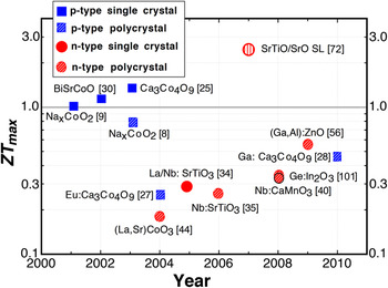
To date, the maximum ZT values achieved in p-type and n-type oxide bulk TE materials are ∼1.0–1.2 and 0.6–0.7, respectively. Furthermore, the ZT of a single crystal is higher than that of polycrystal, and this discrepancy in ZT is notably larger for p-type materials than n-type materials. This observation highlights the importance of grain boundaries and intergranular connections for the TE properties of polycrystals (including nanocomposites).
The interfacial boundary scattering plays a central role in enhancing the ZT of a nonoxide nanocomposite.Reference Medlin and Snyder87 The effective medium theory made it clear that the ZT of a composite can not exceed the best performing constituent if there is no contribution from the interfaces.Reference Bergman and Levy88 Ideally a multifold preferential scattering at interfacial boundaries should be implemented to scatter phonons more effectively than electrons as for a “PGEC” and to scatter those carriers with low mean energy more effectively than those with higher mean energy for a larger |α| and PF in the context of the electron filtering mechanism.Reference Zide, Vashaee, Bian, Zeng, Bowers and Shakouri89, Reference Zebarjadi, Esfarjani, Shakouri, Bian, Bahk and Zeng90 Such multifold preferential scattering mechanisms can be implemented via controlling the physical parameters of the barrier at interfacial boundaries.Reference Medlin and Snyder87
C. Nanocomposite oxides
Note that n-type oxide bulk materials such as SrTiO3 and CaMnO3 have fairly high PF values and their low ZT values are due primarily to high κ l. For example, κ l accounts for ∼80% of κ in SrTiO3. For an all-oxide TE device, higher ZT of n-type materials are required and may be achieved primarily by reducing κ l via the nanostructuring approach. This is the main theme of this section.
1. Nanostructuring and reducing κ l
In several nanostructured nonoxide materials, κ l is found to be lower than the so-called “alloy limit” of bulk thermal conductivity.Reference Li, Wu, Fan, Yang and Marjumdar91–Reference Chiritescu, Cahill, Nguyen, Johnson, Bodapati, Keblinski and Zschack94 Phonons in a material have a temperature-dependent wide spectrum of wavelengths and mean free paths, all of which contribute to κ l. Hence, it is commonly believed that a multiscale structural complexity,Reference Snyder and Toberer95 from the atomic scale alloying and strain fields to the interfacial boundary scattering particular to nanoscale constituents, is required to effectively scatter phonons of a wide range of energies and wavelengths and over a wide temperature range. At present, a main challenge is the lack of quantitative understanding of the contribution from each scattering mechanism and the interplay between these mechanisms. As a result, the present effort is largely trial and error, modeling based on molecular dynamics and nonequilibrium Green’s functions should be conducted in the future.
A recent study of the dependence of grain size and κ l in undoped SrTiO3Reference Koumoto, Wang, Zhang, Kosuga and Funahashi14 shows that κ l decreases nearly linearly with decreasing grain size below 100 nm, and assuming this linearity holds, κ l will reach the alloy limit with a grain size of few nanometer.Reference Cahill, Watson and Pohl96 The grain boundaries scatter phonons at lower temperatures, and the Umklapp phonon–phonon scattering dominates at elevated temperatures. In another study, (Ca,Yb)MnO3 nanoparticles with an average size of ∼50 nm have been prepared using a gas-phase reaction (GPR, or flash creation method) techniqueReference Watanabe, Fukui, Nogi, Kizaki, Noguchi and Miyayama97 and then sintered at 1323 K into bulk sample of about 70% theoretical density. In the sintered sample, the average grain size is 620 nm. The (Ca,Yb)MnO3 GPR-bulk sample exhibits a variable range hopping resistivity behavior, and the detrimental bipolar effect is shifted to higher temperatures compared with the bulk sample prepared by a solid state reaction.Reference Koumoto, Wang, Zhang, Kosuga and Funahashi14
2. Nanocomposite TE oxides
An often used nanocomposite synthesis method is to incorporate a small amount of nanosized secondary phase into a bulk matrix with proved TE performance. For example, the formation of Yb2O3 nanoprecipitates,Reference Zhao, Shi, Chen, Zhang, Bai, Pei and Li98 CeO2 nanoparticle,Reference Alleno, Chen, Chubilleau, Lenoir, Rouleau, Trichet and Villeroy99 and the addition of ZrO2Reference He, Stiewe, Platzek, Karpinski, Muller, Li, Torpak and Muhammed100 into a CoSb3-based bulk matrix has led to improved TE properties. The addition of Ge in In2O3 has led to electron doping via the Ge substitution on the In site along with the formation of In2Ge2O7 precipitates and a reported ZT∼0.45 at 1273 K.Reference Berardan, Guilmeau, Maignan and Raveau101
ZnO-based materials are an important class of TE oxides featured by high μ values on the order of 10–100 cm2/VsReference Tsubota, Ohtaki, Eguchi and Arai54 (one of the highest reported in oxides) and high PFs on the order of 10−3 W/mK2 (comparable to that of SiGe materials). The main challenge is to reduce κ l without deteriorating the PF. Making a solid solution with MgO and NiO has proved to be unsuccessful. Because of very low dopant solubility on Zn site, addition of Al in ZnO more than 2 mol% resulted in the formation of fine precipitates of ZnAl2O4.Reference Tsubota, Ohtaki, Eguchi and Arai54, Reference Katsuyama, Takagi, Ito, Majima, Nagai, Sakai, Yoshimura and Kosuge55 Ohtaki et al. recently reported a co-doping of Al and Ga in ZnO and a ZT∼0.65 at 1273 K in a nanocomposite with a nominal composition of Zn0.96Al0.02Ga0.02O.Reference Ohtaki, Araki and Yamamoto56
Koumoto’s group recently reported the incorporation of nanosized yttria-stabilized zirconia,Reference Wang, Han, Ba, Wang, Wan, Fujinami and Koumoto102 mesoporous silica,Reference Wang, Han, He, Ba and Koumoto103 and potassium titanateReference Wang, He, Ba, Wan and Koumoto104 in Nb-doped SrTiO3 bulk matrix and the impact on the TE properties. The results show that these additions (up to a few wt%) enhance the phonon scattering at grain boundaries, increase the electrical conductivity via promoting the packing density, thus leading to a substantial enhancement of ZT. On the other hand, the thermal and chemical stabilities of nanosized oxide additions in the bulk matrix deserve more investigations. For example, Sr2Ti2SiO8 phase has a tendency to form in the Nb-doped SrTiO3-mesoporous silica composite, though it helps scatter phonons more effectively.Reference Wang, Han, He, Ba and Koumoto103
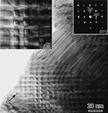
Nanocomposites can be also prepared using an in situ or self-assembly method,Reference Sootsman, Chung and Kanatzidis105 such as spinodal decomposition and matrix encapsulation (“arrested precipitation”) in nonoxide TE materials. Compared to the ex situ method, the in situ method usually leads to more coherent or semicoherent interfacial boundaries that promote μ. Along this line, heat treatment-induced phase separation has been used to prepare Zn(Mn,Ga)O4 nanocomposites.Reference Yeo, Horibe, Mori, Tseng, Chen, Khachaturyan, Zhang and Cheong106, Reference Kosuga, Kurosaki, Yubuta, Charoenphakdee, Yamanaka and Funahashi107 The nanocomposite is comprised of a tetragonal ZnMn1.7Ga0.3O4 phase and a cubic ZnMn0.5Ga1.5O4 phase. As shown in Fig. 5, they are in the form of nanorods and alternately stacked in such a way that the cross-sectional and side views show checkerboard and herringbone patterns, respectively. The average size of each nanorod is ∼4 × 4 × 70 nm3 and the average size of a grain is ∼3 μm. For comparison, a microcomposite composed of ZnMn1.7Ga0.3O4 and ZnMn0.5Ga1.5O4 coarse grains has been prepared with an average grain size ∼3.7 μm and without intragrain nanostructures. The κ l value of the nanocomposite is not only significantly lower than that of the microcomposite but also lower than the value predicted by a simple mixed circuit model.Reference Koumoto, Wang, Zhang, Kosuga and Funahashi14 Further investigation and a comparison with the Hashin–Shtrikman modelReference Hashin and Shtrikman108, Reference Hashin and Shtrikman109 are needed.
Main panel: electron microscopy image of self-assembled nanocheckerboard and nanoherring structures within a Zn(Ga,Mn)O4 grain. Upper-right inset: corresponding electron diffraction pattern indexed with the cubic lattice; upper-left inset: high-resolution image of the checkerboard pattern (the scale bar is 5 nm). (From Ref. Reference Kosuga, Kurosaki, Yubuta, Charoenphakdee, Yamanaka and Funahashi107. Copyright Japan Society of Applied Physics, reproduced with permission.)

IV. OXIDE-BASED THERMOELECTRIC MODULE
Though the ZT values of oxides are mostly lower than the ZT = 1 benchmark, oxide TE modules have been constructed and studied.Reference Matsubara, Funahashi, Takeuchi, Sodeoka, Shimizu and Ueno110, Reference Shin, Murayama, Ikeda and Sago111 Their performance is much lower than expected due mainly to the high contact resistance at oxide/metal electrode junctions, the cracking or exfoliation due to the very different thermal expansion between oxide and metal, and the difficulty of having both p-type and n-type from the same parent compound. The high operating temperatures also make the conventional electrode materials and construction procedure less viable. It was reported that employing mixture of silver paint and 6 wt% oxide powder at the junction achieved lowest contact resistance.Reference Funahashi, Urata, Mizuno, Kouuchi and Mikami112 In Funahashi’s group, a TE module consisting of 108 pairs of oxide legs has been fabricated, using the p-type material Ca2.7Bi0.3Co4O9 and the n-type material Ca0.9Yb0.1MnO3. At a T hot = 1073 K and T cold = 400 K in air, a maximum power output ∼12 W is obtained, yielding a power density of the module higher than 3.0 kW/m2. The maximum value of power density ∼4.2 kW/m2 has been achieved using p-type Ca2.7Bi0.3Co4O9 legs and n-type CaMn0.98Mo0.02O3 legs. In this case, the overall TE conversion efficiency is ∼3%. After cycling, brittle fracture is found in the n-type CaMnO3 legs, but it does not deteriorate the power output, and this problem can be alleviated by optimizing the grain size in the pulverization process.Reference Urata, Funahashi, Mihara, Kosuga, Sodeoka and Tanaka113
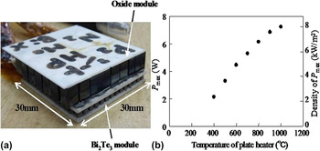
To further increase the power output, a cascade module (segmented module) has been fabricated using 14 pairs of p-type and n-type legs. Alumina substrate is used at one side of the module, forming a so-called half skeleton module (33 × 34.5 × 6.2 mm3). A commercial Bi2Te3 module with dimensions of 30 × 30 × 3.6 mm3 is used [Fig. 6(a)]. Temperature dependence of power output, P max, and the power density of P max are shown in Fig. 6(b). P max and density of P max increase with increasing temperature. At a T hot = 1273 K and T cold = 300 K in air, the density of P max reaches 8 kW/m2, which is twice that of the monolithic oxide module. The temperature at the interface between the oxide and Bi2Te3 modules must be held 453 K or lower to prevent damages to the Bi2Te3 module.
(a) Pictures of oxide/Bi2Te3 cascade module and (b) the dependence of maximum power output on the heater temperature.

V. CONCLUDING REMARKS
The decreasing fossil fuel supplies and their environmental concerns along with the increasing energy demand worldwide impose a pressing need for improved direct thermal–electrical energy conversion via thermoelectricity. The past two decades have witnessed another rapid progress in the field of TEs since the discovery of Bi2Te3 and PbTe bulk materials in 1960s, and as a result, the figure of merit has been almost doubled in heavy element-based TE materials due primarily to the new paradigm of “nanostructured thermoelectrics.”
On the other hand, the history of oxides TEs is fairly short. Nonetheless, the chemical and thermal stability, environmental friendliness, the low cost of raw materials, and chemical versatility are inherent merits of oxide TE materials. As shown in Fig. 7, the efforts in the layer-structured cobaltites, strontium titanate perovskites, and ZnO wurtzites have significantly improved the ZT of oxides in the past decade. Oxides show great potential in the application of power generation at high operation temperatures. Further enhancement of ZT in oxides may hinge primarily upon successful implementation of novel concepts, e.g., spin Seebeck effect,Reference Uchida, Xiao, Adachi, Ohe, Takahashi, Leda, Ota, Kajiwara, Umezawa, Kawai, Bauer, Maekawa and Saitoh114 energy-specific equilibrium,Reference Humphery and Linke115 synergistic nanostrucuringReference Sootsman, Chung and Kanatzidis105, technical advent of high-throughput screening of candidate materials116, discovering new materials, e.g., LaFeAsO1-y117, and advances in theoretical modeling of heat and charge flows in nanocomposites.
The timeline of representative p-type and n-type TE oxides and their maximum figure of merit values. The number in the bracket is the reference number.

ACKNOWLEDGMENTS
J.H. and Y.F.L thank Dr. Don Liebenberg for helpful discussion and the support from a Department of Energy/ Experimental Program to Stimulate Competitive Research (DOE/EPSCoR) Implementation Grant (No. DE-FG02-04ER-46139), and in addition, support from the SC EPSCoR Office/Clemson University cost sharing.