The discovery of phenomena such as high-temperature superconductivity, colossal magneto resistance, spintronic, and multiferroicity has renewed the interest in transition metal oxide systems. The rich variety of physical phenomena in correlated-electron oxides arises from the interactions involving the lattice, orbital, spin, and charge degrees of freedom, which makes these materials attractive candidates for potential applications in fundamental and applied research.[ Reference Bibes and Barthelemy 1 – Reference Yang, Ko and Ramanathan 3 ]
The rare earth nickelates (RNiO3) as correlated systems have received much attention owing to the strong relation between their structural and physical properties.[ Reference Medarde 4 ] Any RNiO3 bulk material except LaNiO3 exhibits either a sharp first-order insulator–metal transition (IMT) or a second-order transition at a temperature (T IMT). For example, the IMT of compounds with R = Pr, Nd, Sm, and Eu occurs at 135, 200, 400, and 460 K, respectively. Moreover, for compounds mixing Sm and Nd such as Sm0.6Nd0.4NiO3 (SNNO), T IMT is 320 K, which is closer to room temperature. The increase of TIMT when decreasing the R cation mass is related to the changes of the Ni–O–Ni bond angle and of Ni–O bond length, which in turn determine the electronic structure.[ Reference Catalan 5 ] At low temperature, the insulating state is characterized by the presence of in-equivalent Ni sites in the monoclinic structure, possibly associated with the charge disproportionation.[ Reference Staub, Meijer, Fauth, Allenspach, Bednorz, Karpinski, Kazakov, Paolasini and d'Acapito 6 – Reference Stewart, Brownstead, Liu, Kareev, Chakhalian and Basov 8 ] The angle bending θ Ni−o−Ni straightens in the bandwidth (W), hence leading to close the gap between O2p and Ni3d orbitals.
From a technological point of view, the materials with IMT around room temperature, such as SNNO in solid solution, can pave the way for many applications, including infrared uncooled bolometers, sensors, and optical and electrical switches.[ Reference de Almeida, Deep, Lima, Khreobtov, Malyarov and Neff 9 – Reference Markov, Marvel, Conley, Miller, Haglund and Weiss 11 ] However, the epitaxial strain plays a crucial role in the IMT of RNiO3. Several studies reported that biaxial compressive (tensile) strain might lead to the decrease or the increase of T IMT, or to the vanishing of the IMT.[ Reference Meyers, Middey, Kareev, van Veenendaal, Moon, Gray, Liu, Freeland and Chakhalian 12 – Reference Liu, Kareev, Gray, Kim, Ryan, Dabrowski, Freeland and Chakhalian 14 ] In this work, the influence of the epitaxial strain from compressive to tensile is characterized on SNNO thin films deposited on three types of substrates. It is found that the valence state of Ni and the Mott transition temperature are both very sensitive to the epitaxial strain. We have demonstrated that the conductivity of the SNNO films at low temperatures is dominated by the Mott variable-range hopping (VRH) mechanism rather than the thermal activation. As the film thickness increases, strain relaxation occurs and the films then exhibit an IMT closer and closer to the T IMT bulk value of 320 K.
Bulk SNNO crystallizes in the orthorhombic Pbnm structure with a O = 5.35 Å, b O = 5.41 Å, and c O = 7.583 Å ,[ Reference Nikulin, Novojilov, Kaul, Mudretsova and Kondrashov 15 ] and the corresponding lattice parameter in pseudo-cubic notation is a p = 3.802 Å. In the present work, SNNO thin films were grown by pulsed laser deposition on (001) SrLaAlO4 (SLAO) and (001) LaAlO3 (LAO) substrates. They are subjected to a compressive strain due to the lattice mismatch of − 1.24% and −0.5%, respectively. In contrast, films deposited on (001) SrTiO3 (STO) are under large tensile strain (+2.6%). A KrF excimer laser (wavelength of 248 nm, laser fluence of 2 J/cm2 and repetition rate of 5 Hz) was used to ablate a stoichiometric target (99.99%, Kurt J. Lesker). During the deposition, the substrate temperature was fixed at 600 °C under an oxygen pressure of 300 mTorr. The SNNO films were subsequently annealed under oxygen pressure for 30 min at the growth temperature. The SNNO thin-film thicknesses were measured to be 8.5 ± 0.4, 16 ± 0.2, and 63 ± 0.2 nm, respectively, using calibrated x-ray reflectivity and cross-sectional transmission electron microscopy. The films structure and the epitaxial relationship with the substrates were characterized by four-circle PANanalytical X'Pert Pro diffractometer with a Cu Kα source, while the surface morphology was examined by atomic force microscopy (AFM). The temperature-dependent resistivity of the SNNO thin films was measured by using four contacts in Hall configuration. Metallic contacts of Cr (10 nm)/Cu (600 nm)/Au (100 nm) were deposited by electron beam evaporation. The resistivity measurement was performed at temperatures varying from 4 to 400 K at a cooling/warming rate of 1 K/min.
Figure 1(a) depicts the x-ray θ − 2θ patterns of 63 nm SNNO thin films on SLAO, LAO, and STO substrates, respectively. The sample on LAO only yields the (00L) diffraction peaks of LAO due to the very small lattice mismatch between SNNO and LAO. The diffraction patterns of the SNNO films on STO and SLAO substrates reveal that they are highly (00L) oriented single phase. The x-ray diffraction (XRD) ϕ scans performed on the (111), (103), and (101) plans of SNNO films [Figs. 1(b)–1(d)] display a clear fourfold symmetry well matching those of the substrates, which demonstrates the in-plane orientation aligned with the substrate. To further elucidate the strain effect, reciprocal space mapping was carried out around the (103) Bragg reflection of SNNO films [as an example, see Fig. 1(e)]. The in-plane and out-of-plane lattice parameters of SNNO on STO were estimated to be 3.843 and 3.764 Å, respectively, which indicates that the film is partially strained. For the SNNO thin film on SLAO, the unit-cell parameters were determined to be a // = 3.85 and c ⊥ = 3.799 Å. In contrast to what is expected for a compressive strain, the larger in-plane lattice constant of SNNO films compared with bulk (3.802 Å) suggests that the relaxation of compressive strain is probably chemically driven through the formation of oxygen vacancies.[ Reference Conchon, Boulle, Guinebretiere, Girardot, Pignard, Kreisel, Weiss, Dooryhee and Hodeau 16 ] The surface of SNNO on SLAO [Fig. 1(f)] shows rounded grains on a flat surface and the root-mean-square surface (rms) roughness is 3.2 nm. In contrast, the SNNO films grown on LAO [Fig. 1(g)] and STO [Fig. 1(h)] exhibit atomically smooth surface with rms roughness of 0.3 and 0.5 nm, respectively.
(a) X-ray diffraction pattern of 63 nm SNNO thin films grown on different substrates. (b–d) XRD ϕ scan of the (111), (103), and (101) peaks of SNNO films on STO, LAO, and SLAO substrates, respectively. (e) Reciprocal space map around (103) reflections for SNNOpc film and STO substrate. (f–h) AFM images presenting the surface morphology of 63 nm SNNO thin films deposited on SLAO, LAO, and STO substrates, respectively.

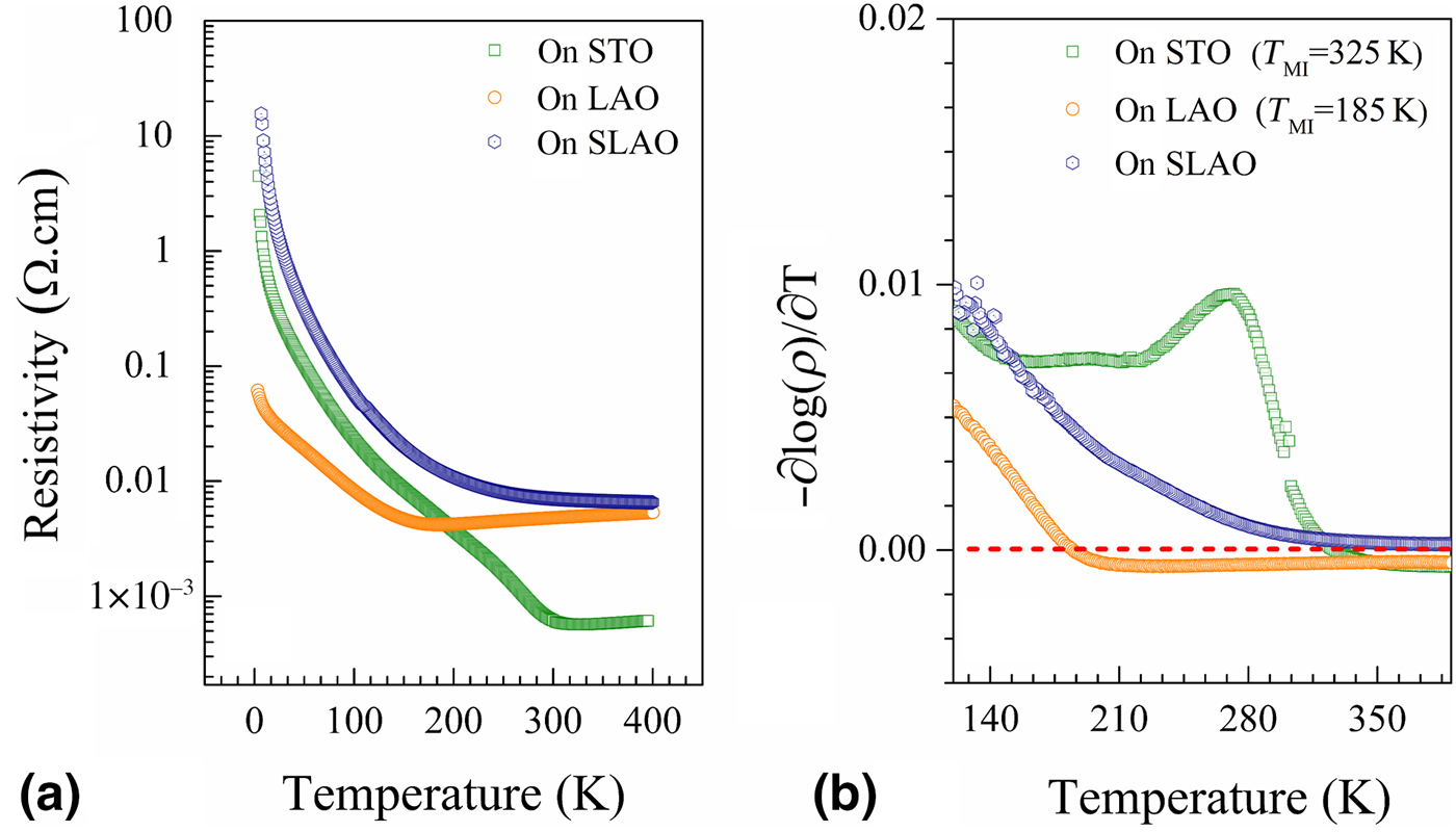
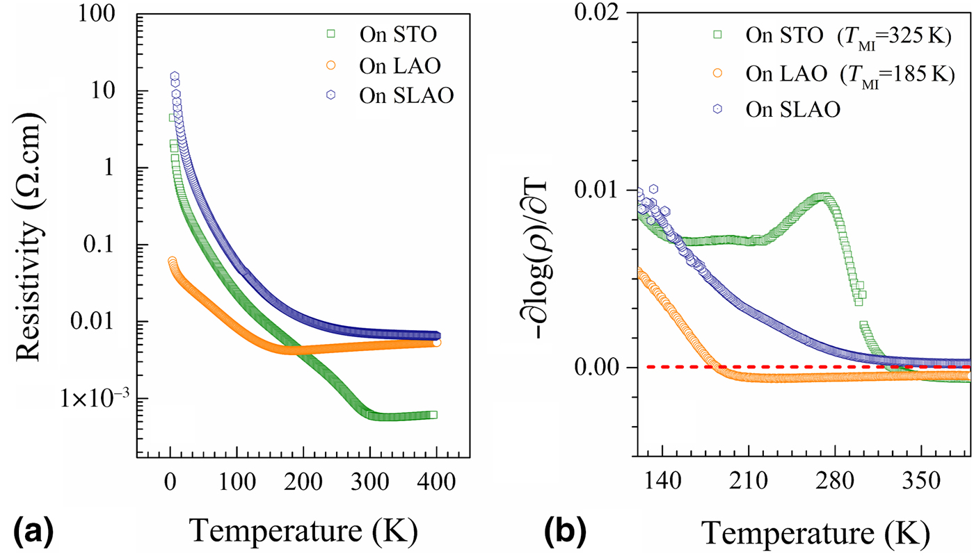
Figure 2(a) shows the electrical resistivity (ρ) as a function of temperature for 63 nm-thick SNNO films grown on different substrates. The film deposited on STO undergoes a very sharp IMT at 325 K (i.e., very close to the bulk transition temperature) as indicated by the sign change of –∂Log (ρ)/∂T [Fig. 2(b)]. In the case of small compressive strain, i.e., for LAO substrate, a drastic drop of the T
IMT value to 185 K takes place. This temperature lies below that of the bulk sample (~322 K) and is also lower than those previously reported for SNNO/LAO (282, 320, and 318 K).[
Reference Huang, Luo, Yang, Yun, Yang, Meng, Wang, Hu, Bao, Lu and Gao
17
–
Reference Girardot, Kreisel, Pignard, Caillault and Weiss
19
] On the other hand, the SNNO film grown on SLAO does not exhibit any IMT, but rather a semiconducting behavior with three orders of magnitude change of the resistivity between 4 and 400 K. Recently, much work has been dedicated to study the epitaxial strain on IMT of RNiO3 thin films. For example, the electrical resistivity of the NdNiO3 (NNO) thin films reveals that the IMT behavior is greatly affected by applying the compressive strain on the films. Indeed, it has been shown that the IMT temperature shifts at low temperature as the compressive strain increases.[
Reference Liu, Kargarian, Kareev, Gray, Ryan, Cruz, Tahir, Chuang, Guo, Rondinelli, Freeland, Fiete and Chakhalian
20
,
Reference Mikheev, Hauser, Himmetoglu, Moreno, Janotti, Van de Walle and Stemmer
21
] Under larger compressive strain
 $\varepsilon _{xx} = - 1.3\% $
(NNO/SLAO), the insulating state is completely suppressed and the film exhibits a metallic phase. Recent theoretical calculations conclude that the compressive strain is accommodated by straightening the Ni–O–Ni angle, which in turn increases the orbital overlap and modifies the bandwidth. Such bond straightening leads to a continuous shift of the IMT and stabilizes a metallic paramagnetic state.[
Reference Catalano, Gibert, Bisogni, Peil, He, Sutarto, Viret, Zubko, Scherwitzl, Georges, Sawatzky, Schmitt and Triscone
22
] On the other hand, the tensile strain has been associated with increased oxygen vacancies, which leads to the smeared or the annihilation of the IMT, as observed for epitaxial NNO on MgO,[
Reference Catalan, Bowman and Gregg
23
] Sm0.5Nd0.5NiO3 on STO,[
Reference Zhang, Gardner, Chen, Singh and Hong
24
,
Reference Zhang, Chen, Gardner, Koten, Shield and Hong
25
] and SmNiO3 (SNO) on STO.[
Reference Conchon, Boulle, Guinebretiere, Girardot, Pignard, Kreisel, Weiss, Dooryhee and Hodeau
16
] The SNNO films grown on SLAO substrates exhibit a larger unit-cell volume (56.31 Å3), suggesting the increase of the oxygen vacancies. This volume expansion could change the Ni–O bond distance and decrease the Ni–O–Ni bond angle, which in turn would result in reduced orbital overlap, and consequently would enhance electron localization leading to the vanishing of the IMT. In the case the SNNO film on STO substrates, the pseudo-cubic unit-cell volume is ~ 55.58 Å3, which is close to the unit-cell volume of bulk SNNO (54.95 Å3) prepared at high oxygen pressure. This result indicates that the amount of oxygen vacancies in SNNO films is smaller, resulting in the occurrence of the IMT at a temperature very close to the bulk transition temperature.
(a) Resistivity of 63 nm SNNO films grown on different substrates as a function of temperature. (b) Derivative of resistivity [–∂log (ρ)/∂T].
The disorder in materials leads to the formation of electronic trap states in the gap[ Reference Gantmakher 26 ] where the wave function amplitudes of the localized states decrease rapidly with the distance. At low temperatures, the energy and the phonon density are considerably reduced. The charge transport between energetically favorable sites can lead to VRH conduction that can become the dominant conduction mechanism. For three-dimensional (3D) systems, Mott has assumed that the density of states near the Fermi level is constant and it was then demonstrated that the VRH is described by[ Reference Mott 27 – Reference Mott and Davis 29 ]
 $$\sigma = \sigma _{\rm 0}T^{ - 1/2}{\rm exp\;} \left[ { - {\left( {\displaystyle{{T_{\rm M}} \over T}} \right)}^{1/4}} \right],$$
where
 $$\sigma _0T^{ - 1/2} = 3e^2\gamma _{{\rm ph}}\left[ {\displaystyle{{N(E_{\rm F})a} \over {8\;\pi k_{\rm B}}}} \right]^{1/2}{\rm et\;} T_{\rm M} = \displaystyle{{18.1} \over {k_{\rm B}N(E_{\rm F})a^3}}.$$
Here, σ is the electrical conductivity of the film, T
M is the Mott characteristic temperature,
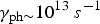 $\gamma _{{\rm ph} \sim}10^{13}\; s^{ - 1}$
is the optical phonon frequency calculated from the Debye temperature,[
Reference Paul and Mitra
30
]
a is the localization length of the relevant electronic wave function, k
B is the Boltzmann constant and N(E
F) is the electron density of states of the Fermi level in the absence of electron–electron interaction. The Mott's parameters, i.e., the most probable hopping distance and the average hopping energy are given, respectively, by[
Reference Paul and Mitra
30
]
 $$R = \left[ {\displaystyle{{9a} \over {8\pi k_{\rm B}TN(E_{\rm F})}}} \right]\; \;{\rm and}\;\; W = \displaystyle{3 \over {4\pi R^3N(E_{\rm F})}}.$$
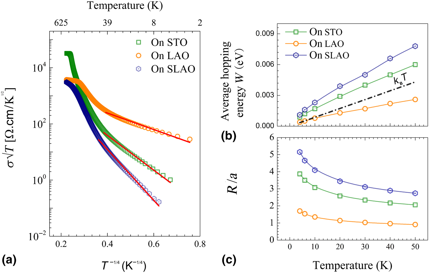
Figure 3(a) shows
 ${\rm Log\;} (\sigma \surd T)$
versus T
−1/4 for SNNO thin films grown on different substrates. It is clearly seen that for sufficiently low temperatures (~4 and ~50 K), i.e., large
 $T^{ - 1/4},{\rm Log\;} (\sigma \surd T)$
displays a very good linear dependence each curve corresponding to a specific slope T
M. This suggests that the conductivity of the investigated samples obeys Mott's relation. However, a clear deviation from the linear fit occurs at high temperature where the thermal activation is probably the dominant conduction process. Using the fitted values of T
M, our experimental values of N(E
F) are found to be 6.3 × 1024, 2.2 × 10²¹, and 1.1 × 1025cm−3eV−1 for the films grown on STO, LAO, and SLAO, respectively. Let us note that the variation of N(E
F) is consistent with the oxygen vacancies due to strain relaxation in the films. However, these values are three or four orders of magnitude higher than those obtained by Zhang et al.[
Reference Zhang, Gardner, Chen, Singh and Hong
24
] This discrepancy is most likely due to the different thickness of the samples and deposition conditions. Indeed, when increasing the film thickness, progressive strain relaxation takes place and gives rise to the density of defects (dislocations, cracks, oxygen vacancies, etc.), which could lead to the increase in the density of localized state. Moreover, the deposition conditions such as substrate temperature and oxygen pressure can affect the chemical composition, structural and morphologic properties of the film, which in turn may change the density of state of impurity levels at Fermi level.
(a) Representation
 $\sigma \sqrt T $
versus T
−1/4 for 63 nm-thick SNNO samples. The red solid lines are obtained from linear fitting of the temperature below 40 K. (b, c) Temperature dependence of the average hopping energy W (eV) and of the ratio R/a for SNNO thin films.
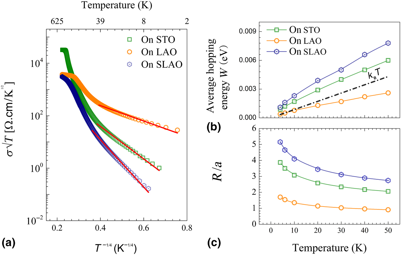
According to the Mott's requirements, 3D VRH is achieved when W > k B T and R/a > 1.[ Reference Paul and Mitra 30 ] Therefore, as shown in Figs. 3(b) and 3(c), these criterions are satisfied for the SNNO films on SLAO and STO substrates. These results are in agreement with previous studies on RNiO3 systems.[ Reference Xiang, Zhong, Duan, Tang, Hu, Yang, Zhu and Chu 31 , Reference Ramadoss, Mandal, Dai, Wan, Zhou, Rokhinson, Chen, Hu and Ramanathan 32 ] In contrast, for SNNO on LAO, the conditions are not fulfilled and therefore VRH does not apply.
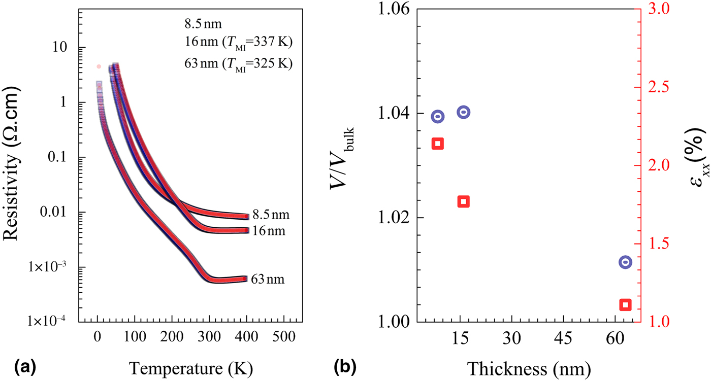
In order to characterize the effect of strain relaxation, we determined the electrical resistivity of SNNO films with different thicknesses. Figure 4(a) shows the film resistivity as a function of temperature for 8.5, 16, and 63 nm SNNO films on STO. For the 8.5 nm-thick film, no IMT is observed. Instead, the resistivity exhibits a semiconducting-like temperature dependence over the whole temperature range investigated. The 16 nm film displays an IMT at 337 K, associated to a change of resistivity by three orders of magnitude. In the case of the thickest film (63 nm), we observe a very sharp IMT at 325 K, which is very close to the bulk transition temperature. Moreover, when further increasing the film thickness, the resistivity of the metallic state decreases from 4.62 × 10⁻³ to 5.8 × 10⁻⁴Ω.cm at 350 K.
(a) Resistivity versus temperature for SNNO films with different thicknesses grown on SrTiO3. (b) Left axis: the ratio of the unit-cell volume of the film to that of bulk SNNO as a function of thickness. Right axis: thickness dependence of the in-plane film strain ε xx .
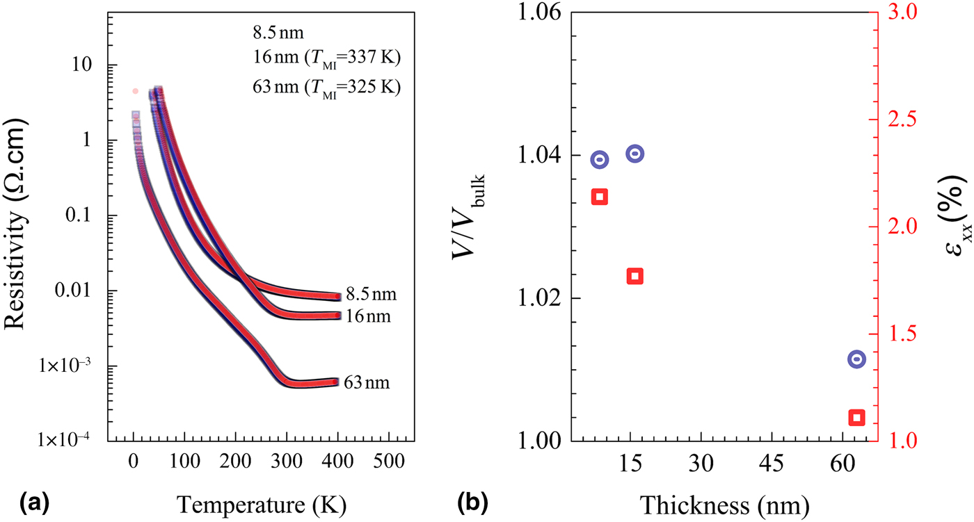
To further understand the presence or the absence of an IMT depending on the thickness for SNNO on STO, the ratio of the unit-cell volume of the film over bulk SNNO is plotted on the left side of Fig. 4(b) together with in-plane film strain, ε
xx
, defined as ε
xx
= (a
// − a
0)/a
0 on the right side. Here, a
// and a
0 are the in-plane and unstrained film lattice parameters,[
Reference Hauser, Mikheev, Moreno, Hwang, Zhang and Stemmer
33
] respectively. The unit-cell volume is the smallest for the 63 nm film and it is also the closest to that of bulk SNNO. This suggests that the amount of oxygen vacancies is relatively low, which accounts for the existence of an IMT at 325 K. In the case of the thinnest film (8.5 nm), a clear increase of the unit-cell volume and a large amount of strain
 $(\varepsilon _{xx} = 2.24\% )$
is observed, suggesting that the in-plane tensile strain enhances the degree of NiO6 octahedral tilts, which results in reduced orbital overlap and thus leads to a second-order transition. Finally, at an intermediate thickness (16 nm-thick), the unit-cell volume is similar to that of the 8.5 nm-thick film. However, the amount of strain
 $(\varepsilon _{xx} = 1.74\% )$
is low, thus resulting in the increase of both the transition temperature and the metallic state resistivity.
Once the thickness decreases, the transition temperature of the SNNO samples shifts to slightly higher values suggesting enhanced electron localization. The relaxation of tensile strain in SNNO films grown on STO changes the lattice constants, which results from modifications of the Ni–O length and/or of the Ni–O–Ni band angle. Such variations of the SNNO unit cell determine the delocalization bandwidth of the system. Similar thickness dependence in T IM was observed in NNO[ Reference Catalan, Bowman and Gregg 23 ] and Sm0.5Nd0,5NiO3 [ Reference Zhang, Gardner, Chen, Singh and Hong 24 ] films on STO substrate. Furthermore, Zhang et al.[ Reference Zhang, Gardner, Chen, Singh and Hong 24 ] concluded that extrinsic effects such as oxygen vacancies induced by strain relaxation do not drive enhanced electron localization in Sm0.5Nd0.5NiO3 on STO. They associated the different electrical transport characteristics to strain modulation of the Ni–O bond length and Ni–O–Ni bond angle.
In conclusion, the electrical transport properties of epitaxial SNNO exhibit a significant dependence on the oxygen vacancies. Indeed, tensile in-plane strain stabilizes the structure and lowers the quantity of oxygen vacancies resulting in the occurrence of the IMT at 325 K. In contrast, large compressive strain induces the creation of oxygen vacancies and annihilates the IMT. Small compressive strain (LAO substrate) induces the drastic reduction of T IMT to 185 K. By examining the electrical transport data, we uncovered that the conductivities of the SNNO films follow the Mott-VRH law only for growth on SLAO and STO substrates but not on LAO. Finally, once the tensile strain relaxation is established by increasing the film thickness, the IMT of SNNO samples decreases gradually to that of the bulk value.