


1. Introduction
A number of anomalous processes take place in current-carrying laboratory plasma. It is generally accepted that anomalous phenomena include: accelerated plasma diffusion across an insulating magnetic field, decrease of conductivity in strong fields, generation of fast particle fluxes and microwave emission. A feature of anomalous processes in magnetically insulated diodes of electron accelerators is that all these processes occur almost simultaneously – in the stage of violation of the plasma magnetic insulation, which is accompanied by a sharp drop in the voltage applied to the diode. In tokamaks, current interruption also correlates with the generation of fast particles. The method of confining charged particles with the help of a magnetic field (Hull Reference Hull1921) is widely used in various technical devices. This method makes it possible to reliably hold charged particles of the same type in space. However, numerous attempts to use the method of magnetic isolation for confinement plasma over many years did not give positive results.
Bohm & Gross (Reference Bohm and Gross1949) discovered that plasma diffusion has an anomalous character, i.e. the plasma is ejected onto the chamber walls in the direction across the longitudinal magnetic field much faster than they assumed according to classical calculations. Many theoretical models have been proposed to explain the mechanism of anomalous plasma diffusion. There is an assumption that Rayleigh–Taylor hydrodynamic instability significantly affects the anomalous plasma transport onto the chamber walls. This type of instability is volumetric in nature, so the plasma must be deposited on the walls of the chamber as one unit. However, strong fields, plasma bunches and fluxes of fast particles in the direction perpendicular to the longitudinal magnetic field have been detected in plasma magnetic confinement experiments (Gorev et al. Reference Gorev, Dolgachev, Zakatov, Oreshko and Skoryupin1985; Oreshko Reference Oreshko1991, Reference Oreshko2012). The impact of bunches and fluxes of fast particles on the chamber walls was local. Plasma channels were found between the plasma and the chamber walls in these experiments. These data give reason to believe that instability is established in plasma associated with fluxes of charged particles and the emergence of structures with a strong field in it. There are fluxes of particles in plasma, with the help of which generation of strong fields and anomalous particle transport take place.
In the theory of high-current self-contracting discharges (z-pinches), it was commonly believed that, with the help of a strong current that creates an azimuthal magnetic field, it is possible to compress the plasma to certain minimum dimensions and, as a result of energy concentration, carry out a controlled fusion reaction in it (Bishop Reference Bishop1958; Rose & Clark Reference Rose and Clark1961). The magnetic self-isolation method does not require the use of bulky solenoids. However, in experiments on high-current self-contracting discharges, it was also not possible to carry out the fusion reaction. In experiments on pinch discharges, neutrons were registered, the generation mechanism of which has an accelerative character (Artsimovich Reference Artsimovich1964; Vikhrev & Korolev Reference Vikhrev and Korolev2007).
It is generally accepted that failures in experiments on controlled nuclear fusion are caused by runaway electrons. Runaway electrons are responsible for interruption and disruption of current in tokamaks (Smith et al. Reference Smith, Helander, Eriksson, Anderson, Lisak and Andersson2006; Fülöp, Smith & Pokol Reference Fülöp, Smith and Pokol2009) and stellarators (Linder et al. Reference Linder, Papp, Fable, Jenko and Pautasso2021). Note that there are a large number of theoretical models for the appearance of runaway electrons in the plasma of tokamaks. The generation of large-scale electromagnetic structures (blobs) in plasma has been studied (Bodi, Smolyakov & Krasheninnikov Reference Bodi, Smolyakov and Krasheninnikov2009). Runaway electrons exist in the solar corona and in the solar wind (Vocks & Mann Reference Vocks and Mann2003).
A number of papers have been devoted to the study of plasma conductivity at low values of applied voltage. However, there is very little information about the nature of conductivity in strong electric fields. As noted in Dreicer (Reference Dreicer1959), when the electric field strength in the plasma exceeds the critical value, Ohm's law $\boldsymbol{j} = \sigma \boldsymbol{E}$ is violated. The phenomenon of anomalous resistance is explained by the presence of runaway electrons from collisions in the plasma (Dreicer Reference Dreicer1959). Runaway electrons have been detected in a reversed field pinch (O'Connell et al. Reference O'Connell2003). The anomalous resistance exceeds the resistance value determined by Coulomb pair collisions. Dependences of the plasma conductivity on the electric field strength and the yield of conductivity on the plateau were found by Demidov, Elagin & Fanchenko (Reference Demidov, Elagin and Fanchenko1967). The increase of resistance in the plasma in this paper is explained by the rocking of intense plasma waves. It is generally believed that the anomalous resistance is due to the ion-sonic instability of the current that flows in the plasma (Demidov et al. Reference Demidov, Elagin and Fanchenko1967; Kalinin et al. Reference Kalinin, Lin, Rudakov, Ryutov and Skoryupin1970). An increase in plasma resistance is observed in plasma-focus discharges at the stage of collapse. At this stage, as is known, ‘hot’ spots appear, fast deuterons are generated with an energy sufficient to overcome the Coulomb potential barrier and subsequent neutron emission, as well as the emission of intrinsic microwave radiation (Bostick, Nardi & Zucker Reference Bostick, Nardi and Zucker1976). Anomalous resistance is recorded in beam-plasma discharges and in plasma-erosion opening switch (PEOS), which are used to sharpen the pulse in high-current electron accelerators (Weber et al. Reference Weber, Commisso, Cooperstein, Grossmann, Hinshelwood, Mosher, Neri, Ottinger and Stephanakis1987). Emission of microwave radiation was also registered in PEOS. It was noted in Bazelyan & Raizer (Reference Bazelyan and Raizer1998) that an ionized channel in a spark discharge has a falling volt–ampere characteristic. The arc discharge also has a volt–ampere characteristic with a falling section.
The phenomenon of anomalous resistance served as the basis for the development of the concept of turbulent plasma heating (Zavoiskiy & Rudakov Reference Zavoiskiy and Rudakov1967). The paradox is that all anomalous processes in the plasma occur simultaneously. In magnetically isolated diodes of accelerators, anomalous resistance (Oreshko Reference Oreshko2000) and anomalous diffusion (Gorev et al. Reference Gorev, Dolgachev, Zakatov, Oreshko and Skoryupin1985) appear simultaneously at the stage of violation of the magnetic insulation of the diode. Note that at this stage there is anomalous plasma diffusion across the longitudinal magnetic field and the plasma is a source of microwave emission in the wavelength range $3 \le \lambda \le 6\ \textrm{cm}$ . It turned out that it is impossible to heat the plasma in the state of anomalous diffusion using so-called ‘turbulent heating’. The concept of turbulent plasma heating turned out to be erroneous.
The purpose of this article was to give an explanation from a unified standpoint for all the anomalous phenomena that exist in a current-carrying laboratory plasma.
Before proceeding to the presentation of the main results, it is necessary to dwell on the ion-acoustic model of anomalous resistance, which, according to theorists, generates the so-called ion-acoustic turbulence in plasma.
2. On ion-acoustic interpretation of anomalous resistance
The theoretical explanation of the phenomenon of anomalous resistance given in Rudakov & Korablev (Reference Rudakov and Korablev1966) and Kalinin et al. (Reference Kalinin, Lin, Rudakov, Ryutov and Skoryupin1970) does not stand up to elementary criticism. To explain the phenomenon of anomalous plasma resistance, the ion-acoustic model is used, which, like the ion-acoustic instability, is an elementary error in the theoretical interpretation of experimental results. In the ion-acoustic model (Rudakov & Korablev Reference Rudakov and Korablev1966), the plasma current is limited by the value, in which is the electron charge, is their concentration, and is the ion sound velocity, determined by the expression

in which ${k_B}$ is the Boltzmann constant, ${T_e}$
 is the temperature of the electrons and ${M_i}$
 is the mass of the ions. The subscripts e and i denote an electron and an ion, respectively. The expression defined by formula (2.1) is completely wrong from the point of view of common sense, since the numerator is the electron temperature and the denominator is the ion mass. Instead of the frequency of electron–ion collisions ${\nu _{ei}}$
 , which is included in the Spitzer plasma conductivity formula

the ‘effective frequency’ of electron collisions with ‘ion-acoustic noise’ is introduced:

Since the speed of ‘ionic sound’ is a constant value, the ‘effective frequency’ of the interaction of electrons with noise increases with an increase in the electric field strength. Following Rudakov & Korablev (Reference Rudakov and Korablev1966), an increase in the ‘effective frequency’ in a strong electric field leads to a decrease in the plasma conductivity. It should be noted that none of the experimenters found the so-called ‘ionic sound’ in the experiments. The ionic sound model has nothing to do with the real phenomenon that takes place in a plasma. Noise was recorded many years ago when the upper bandwidth of the oscilloscopes used in experiments was very low. It was proposed to cut such noises with the help of radio engineering filters (Artsimovich Reference Artsimovich1964). The question remains unanswered: how can instrumental noise affect the transfer coefficient, which is determined by the density of electrons and the frequency of their collisions with particles, decreasing with increasing electric field strength, and not increasing as the ‘effective frequency’ according to the model (Artsimovich Reference Artsimovich1964)? The real reasons for the decrease in plasma conductivity, its anomalous diffusion across the magnetic field and the appearance of fast particle fluxes in discharges can only be established through experiments. The author considers the process of replacing physics by mathematics unacceptable. As correctly noted in a review (Netchitailo Reference Netchitailo2022), physics cannot exist without mathematics, but mathematics should not replace physics.
3. Experimental results in magnetized plasma
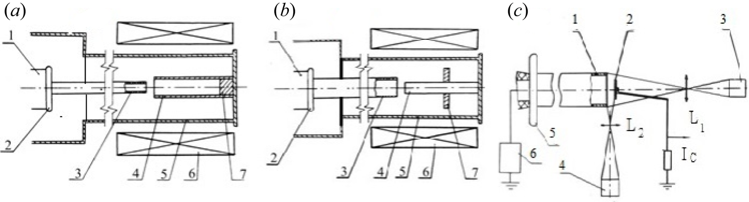
There are a number of experimental data that allow us to give a fundamentally different explanation for the phenomena of anomalous resistance and diffusion, which is not associated with either ion sound or ion-acoustic turbulence (Oreshko Reference Oreshko1991, Reference Oreshko2000, Reference Oreshko2012). A correct explanation of anomalous phenomena in a magnetized plasma can be given with the help of experimental results obtained on a high-current electron accelerator of the microsecond range of duration (PN-4M) (Dolgachev, Zakatov & Oreshko Reference Dolgachev, Zakatov and Oreshko1983). Plasma generation in such accelerators is carried out as a result of explosive emission, and the acceleration of electrons occurs under the action of an electric field inside a magnetically insulated diode. The plasma is magnetized and current-carrying. Schemes of direct and reversed coaxial magnetically insulated diodes are given in figures 1(a) and 1(b), respectively. In a direct diode, the cathode diameter is smaller than the anode diameter, and vice versa in a reversed diode.
The scheme of direct (a) and reversed (b) magnetically isolated diodes used in accelerators of the microsecond range of duration and the scheme of experiment to study the motion of the cathode plasma in the magnetically insulated diode of the accelerator (c). Designations in (a,b): 1, bushing insulator; 2, flange for mounting electrodes; 3, cathode; 4, anode; 5, diode chamber; 6, solenoid of insulating magnetic field; 7, graphite collector. Designations in (c): 1, anode; 2, cathode; 3, electro-optical converter (EP-15); 4, electro-optical streak camera (Kadr-2 SF); 5, flange for mounting electrodes; 6, pulse voltage generator; L 1, L 2, optical lenses; Ic, shunt for current measurement. The diode chamber in (c) is not shown.

In order to study the motion of the plasma, experiments were carried out in the direct and reversed magnetically insulated diodes of the electron accelerator. The scheme of the experiment on the study of plasma in a direct magnetically insulated diode is given in figure 1(c). The diode vacuum chamber and solenoids are not shown in this figure. Diode electrodes made of stainless steel were located inside the diode chamber in the region of a uniform insulating magnetic field with an induction of 10 kGs. The cathode was in the form of a disk. Its diameter was 32 mm; the anode was tubular. The outer diameter of the anode was 50 mm and the inner diameter was 48 mm. A graphite collector was installed inside the anode at a distance of 35 cm from its cut. The diode chamber was evacuated by means a diffusion pump to $2 \times {10^{ - 5}}\ \textrm{Torr}$ . A high-voltage pulse of positive polarity was applied to the tubular anode after starting the Marx generator. The polarity at the cathode was negative. As a result of the explosive emission, a cathode plasma appeared and an electron current was generated in the diode. The plasma density in such diodes is ${10^{15}}\ \textrm{c}{\textrm{m}^{ - 3}}$
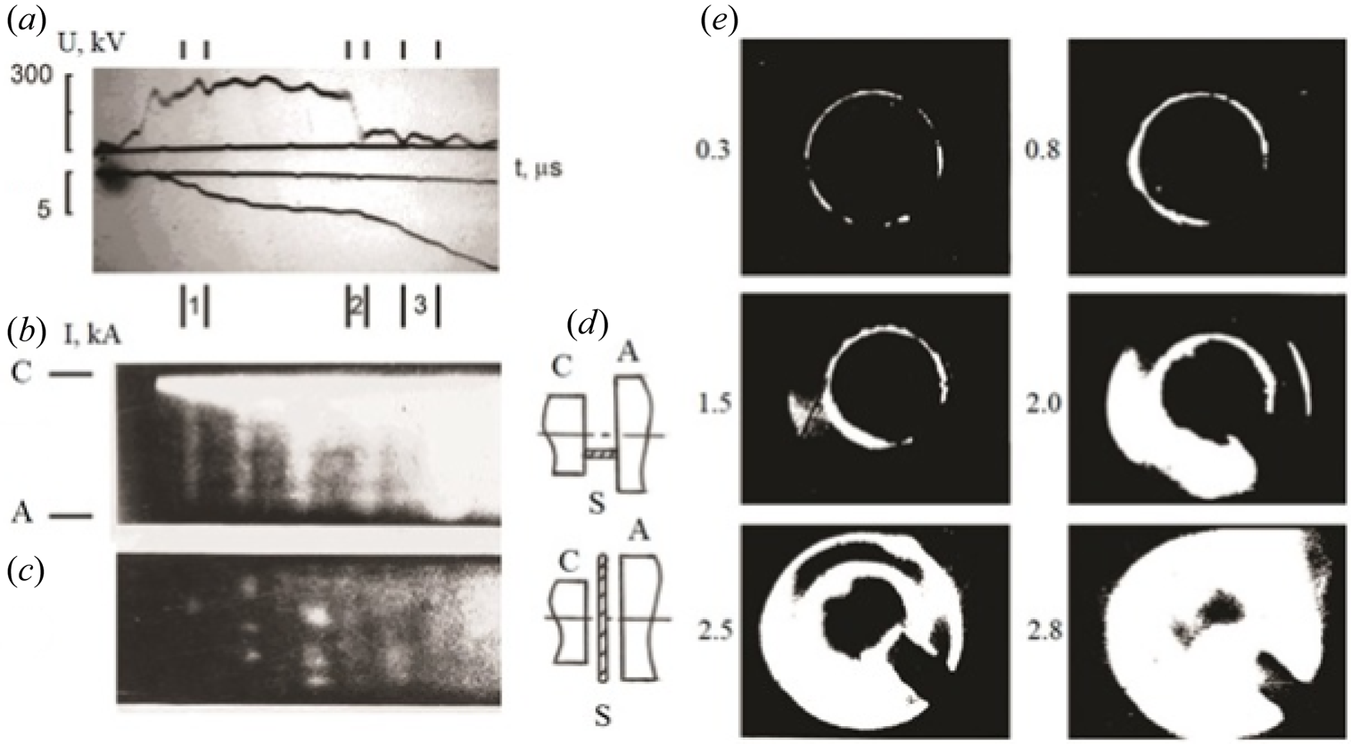
 and the temperature is 5 eV (Bekefi, Orzechowski & Bergeron Reference Bekefi, Orzechowski and Bergeron1975). A longitudinal magnetic field was used, which was created using solenoids for confining the cathode plasma from expanding in the radial direction. The current and voltage in the discharge were measured, respectively, by a shunt and a voltage divider, which were made of low-inductance TVO-type resistors. The velocity of the plasma movement was determined from the propagation of its glow using a streak camera with continuous scanning (Kadr-2 SF). The plasma glow was cut out using a slit both along the diode axis and across its axis (see figure 2d). The use of an EP-15 electro-optical converter installed in the end part of the diode chamber made it possible to register the radial motion of the plasma. Typical wavefronts of the applied voltage U and the current I generated in the diode are given in figure 2(a). The plasma glow scans for two positions of the slit are given in figures 2(b) and 2(c).
Experimental results. (a) Typical wavefronts of applied voltage (upper trace) and current (lower trace). (b,c) Plasma glow image scan for the specified positions of the slit. (d) Region of the interelectrode gap, which was cut out by the entrance slit of the electro-optical camera. (e) Images of the plasma glow in a plane perpendicular to the diode axis (in the radial direction) for six time intervals. Start of EP-15 electro-optical converter relative to the beginning of voltage growth: 0.3 μs; 0.8 μs; 1.5 μs; 2.0 μs; 2.5 μs; 2.8 μs. Exposure: 500 ns. Designations: A, anode; C, cathode; S, position of entrance slit of the streak camera in the gap. Time markers on wavefronts: 0.5 μs.

Analysis of plasma glow sweeps (figure 2b,c) shows that the source of pulsating luminous formations is the cathode plasma moving with a longitudinal velocity equal to $2 \times {10^6}\ \mathrm{cm}\ {\textrm{s}^{ - 1}}$ . These formations move towards the anode region and their speed is equal to $3 \times {10^7}\ \mathrm{cm}\ {\textrm{s}^{ - 1}}$
 . The passage of such structures from the cathode plasma to the anode correlates with applied voltage oscillations and shelves on a typical current wavefront (see figure 2a).
Such structures in plasma can only be electric domains (Oreshko Reference Oreshko1991, Reference Oreshko2000, Reference Oreshko2012). Here and below, an electric domain is understood as a quasi-neutral system as a whole, consisting of a region (layer) with an excess negative charge and a region (layer) with an excess positive charge. The distance between these two regions (layers) of the domain exceeds the Debye screening length. A strong electric field is established between the layers of the electric domain due to the small distance between them (Oreshko Reference Oreshko2001). For the first time, electric domains were discovered in semiconductor plasma by Nobel laureate Gunn (Reference Gunn1963) and in glow-discharge plasma (Mylnikov & Napartovich Reference Mylnikov and Napartovich1975). The electric domain moves under the influence of a strong own electric field. The nucleation of such structures in plasma correlates with an increase in voltage and a decrease in current due to the transition of some plasma electrons from a conducting state to a bound state, to layers of excess negative charge. Identification of the ionic component of the electric domain was carried out by luminescence in the visible part of the spectrum, recorded using a streak camera (see figure 2b,c). The identification of the electronic component of the domain was carried out using shelves on a typical wavefront of the current (see the lower trace in figure 2a). Moreover, the shelves on the current waveform correlate with signal changes on the voltage waveform. These shelves indicate a decrease in plasma current due to the transition of part of the electrons into layers of excess negative charge of electric domains. Electric domains arise in plasma due to the inequality of flows of directed drift of electrons and ions (Oreshko Reference Oreshko2019a).
An analysis of the image of the plasma glow in a plane perpendicular to the diode axis (in the radial direction) for six time intervals shows that the electrical domains are destroyed in the anode region (see figure 2e). The destruction of domains leads to the formation of plasma channels between the anode and cathode plasma. The accumulation of plasma in the interelectrode space leads to a drop in resistance, which becomes sufficient for a short circuit and a sharp drop in the applied voltage. On a typical voltage wavefront (see figure 2e) the voltage drop corresponds to the segment labelled by the number 2. The increase in current in the magnetically insulated diode is due to the growth of the emitting surface when the cathode plasma enters the anode cavity. The area of no image (figure 2e) in the right lower corner is due to the cathode leg with the help of which the cathode was fixed, which was in the field of view of the EP-15 electro-optical converter.
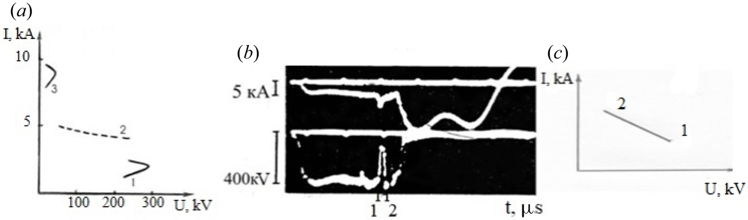
Plasma glow sweeps (figure 2c) show that a multidomain regime is realized in plasma with a delay in the start of their generation. In this mode, each new group of electrical domains appears only after the destruction of the previous group of domains at the anode. It should also be noted that the relationship between moving double layers and potential oscillations was also observed in Q-machine plasma (Song, Merlino & D'Angelo Reference Song, Merlino and D'Angelo1990). In addition to the mode with a delay in the formation of domains and the transit mode in plasma, there can be domain quenching modes, a hybrid mode and a mode of limited space charge accumulation. These modes are discussed in more detail in Oreshko (Reference Oreshko2019a). It should be noted that the electro-optical registration of electric domains in the high-frequency region on powerful experimental facilities is difficult because of the high intensity of plasma radiation. The volt–ampere dependence of the plasma plotted for the three time intervals indicated in figure 2(a) is shown in figure 3(a). From the measurement results shown in figure 2(c), it follows that in the main and post-breakdown stages of diode operation in plasma, there is a multidomain mode with a delay in the generation of electric domains. From the volt–ampere dependence (figure 3a) it follows that in these stages, when electric domains appear, the differential conductivity is negative, i.e. ${\sigma _{e}} = \textrm{d}\sigma /\textrm{d}E < 0$ . It is also negative in the stage of violation of magnetic insulation. It should be noted that the task of visualizing domains at the stage of magnetic isolation violation is difficult: against the background of intense luminescence, it is difficult to distinguish such structures. However, the generation of microwave radiation from the plasma with a frequency f = 5–10 GHz when the magnetic insulation is broken confirms the domain nature of its origin (Gorev et al. Reference Gorev, Dolgachev, Zakatov, Oreshko and Skoryupin1985). It has been experimentally shown and theoretically substantiated that microwave emission from plasma occurs during the generation of electric domains in it (Oreshko Reference Oreshko2006). It should be noted that the microwave emission was registered in earlier experiments (Gunn Reference Gunn1963; Demidov et al. Reference Demidov, Elagin and Fanchenko1967).
(a) The volt–ampere characteristic of the plasma for the indicated time intervals in figure 2(a) in an experiment with a direct diode. (b) Typical wavefronts of current (upper trace) and applied voltage (lower trace). (c) The volt–ampere characteristic corresponding to the presence of a transit mode in the experiment with a reverse diode. The initial moment of time is indicated by the number 1, the final by the number 2. Time marker: 2 μs.

In experiments with a magnetically insulated diode of the reversed type, the mode of passage of the electric domain was discovered on the eve of the stage of violation of the magnetic insulation. The anode diameter was equal to 9 cm and the cathode diameter was 12 cm. The cathode was pushed over the anode at a distance La –c = −3 cm. Typical current and voltage wavefronts are given in figure 3(b). At time t = 3.8 μs from the beginning of the process, there is a feature in the form of a burst, which correlates with a short drop, and then a subsequent increase in voltage. Changes in the magnitude of the voltage correlate with changes in the magnitude of the current. If the current and voltage values for the time interval t = 3.8–4.2 μs from the beginning of the pulse are used to build an ampere–volt dependence, then one can get a section with negative differential conductivity (see figure 3c). After the destruction of the electric domain, the stage of violation of the magnetic insulation begins, accompanied by an increase in the current in the diode and a sharp decrease in the applied voltage. The increase in current in this case can be associated with an increase in conductivity, which occurs when the electric domain is destroyed in the region of the anode plasma. The duration of the half-wave on the voltage burst was 100 ns. If we divide the interelectrode distance by the duration, then we can get the value of the speed, $1.5 \times {10^7}\ \textrm{cm}\ {\textrm{s}^{ - 1}}$ , which is typical for electric domains (Gunn Reference Gunn1964). The differential conductivity of the plasma in the event of a violation of the magnetic insulation is negative. In this experiment, the transit mode of existence of the electric domain was registered. The volt–ampere dependence for the time preceding a sharp drop in voltage is given in figure 3(b). During transit of the electrical domain, the differential conductance is negative, i.e. ${\sigma _d} = \textrm{d}j/\textrm{d}E < 0$
 . The increase in the total current also is associated with an increase in the emitting surface of the plasma when it enters the anode cavity of the coaxial diode.
Electric domains are also observed in an electric discharge near the dielectric surface (Oreshko Reference Oreshko2006). Volt–ampere dependences with negative and zero differential conductivity can be obtained from typical voltage and current wavefronts in the main part of the pulse duration during electrical breakdown (Oreshko Reference Oreshko2006).
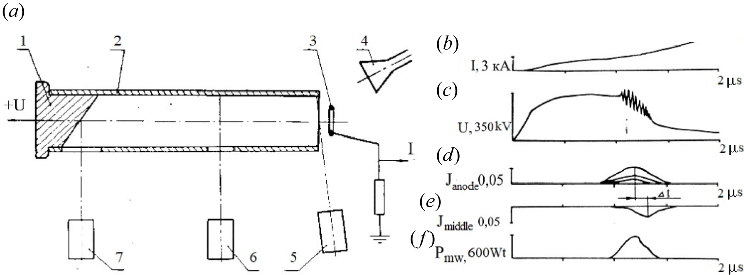
The shape of the voltage pulse applied to the diode depends on the RLC parameters of the electrical circuit and the load – the diode. In a number of experiments, the shape of the voltage pulse differed from that shown in figure 2(a) – it had the shape of a bell (see figure 4c). The stage of violation of magnetic insulation is also characterized by a sharp drop in the applied voltage and the presence of high-frequency oscillations on the voltage oscillogram. In a direct magnetically insulated diode, experiments were carried out to study the motion of plasma inside the anode cavity. The scheme of the experiment is given in figure 4(a). In these experiments, the current of fast electrons to the forward part of the anode was measured by bremsstrahlung using a semiconductor detector (position 5) and microwave plasma emission using a horn (position 4), which was connected by a 3 cm waveguide to a detector of hot carriers. The detector was placed in a Dewar vessel with liquid nitrogen. The vessel was placed outside the vacuum chamber of the diode. Analysis of characteristic wavefronts in figure 4 shows that high-frequency fluctuations in the voltage waveform occur during magnetic insulation failure. The frequency of these oscillations is 5–10 GHz and they correlate with the current of fast electrons to the anode and the generation of microwave emission. The microwave emission was measured in the wavelength range $3 \le \lambda \le 6\ \textrm{cm}$ comparable with the diameters of the cathode and anode. This means that during the violation of magnetic isolation, a high-frequency mode of generation of electric domains takes place, because there are no other sources of microwave emission in the plasma. The presence of microwave radiation and fast electrons and the fact that the plasma velocity inside the anode cavity $(4 \times {10^7}\ \textrm{cm}\ {\textrm{s}^{ - 1}})$
 is characteristic of electric domains indicate that a strong electric field is established in the plasma when magnetic isolation is broken.
(a) Schema of the experiment to study the dynamics of violation of the magnetic insulation of the diode. typical wavefronts of (b) current and (c) applied voltage. Readings of signals from (d) the forward part of the anode and(e) the middle of the anode, as well as (f) the power of microwave emission in the wavelength range $3 \le \lambda \le 6\ \textrm{cm}$ . Designations in (a): 1, collector; 2, anode (D = 5.4 cm, L = 30 cm); 3, cathode (D = 3.2 cm); 4, horn of the microwave emission detector; 5–7, semiconductor detectors equipped with lead collimators.

4. Justification of the mechanism of anomalous plasma resistance
The phenomenon of anomalous resistance was explained due to the effect of runaway electrons from collisions in Dreicer (Reference Dreicer1959). The speed of movement of electrons $\boldsymbol{u}$ is determined by their mobility ${\mu _e}$
 , which depends on the strength of the electric field $\boldsymbol{u} = \mu (E)\boldsymbol{E}$
 and is included in Ohm's law, which is given by the known expression

in which the plasma conductivity for a fully ionized plasma is given by the well-known expression (Spitzer Reference Spitzer2006)

In Ohm's law (equation (4.1)), ${\mu _e} = {\mu _e}(E)$ is the mobility of electrons, which is always greater than the mobility of ions and depends on the strength of the electric field (Raizer Reference Raizer1991). The time of electron–ion collisions is determined by the formula

It follows from Ohm's law (equation (4.1)) that an increase in the electron velocity $\boldsymbol{u} = \mu (E)\boldsymbol{E}$ should lead to an increase in the current density. However, runaway electrons play an important role in the plasma because they contribute to the formation of structures that reduce the plasma conductivity. Further, it will be shown that the created structures not only reduce the conductivity, but also generate turbulence in the plasma due to the created plasma channels and fast particle flows.
As is known, current channelling takes place in plasma – current flows through separate channels. Such current flow is energetically more favourable than current flow across the entire plasma cross-section at equal current density. It is known that the speed of directed motion of electrons in a current-carrying plasma significantly exceeds the speed of ions $({\boldsymbol{u}_e} \gg {\boldsymbol{u}_i})$ . The speed of directional movement of electrons also exceeds the thermal speed. In fact, we can assume that in a current-carrying plasma, electrons move relative to a stationary ionic background. The movement of electrons is due to the presence of an electric field, which is applied between the electrodes. At the moment when the force of friction from the side of the medium is not balanced by the force from the side of the electric field, runaway electrons from collisions appear in the plasma. Their speed exceeds the speed of directional drift. In this case, the electron energy distribution function changes (Golant, Zhilinskiĭ & Sakharov Reference Golant, Zhilinskiĭ and Sakharov1980). The departure or displacement of a group of electrons ‘running away’ from collisions to a distance exceeding the Debye screening length leads to the appearance of a layer of excess negative charge in the near-electrode plasma. In plasma, charge separation occurs. The space charge of such a layer can only be compensated by a layer of excess positive charge, which appears automatically in the region from which the runaway electrons have left. The separation of charges is completed at the moment when the force of attraction between the surplus charged layers of the electrical domain is balanced by the force that leads to the separation of charges. An electric domain with a strong field appears in the plasma, which differs from the double layer in that it moves at a high speed relative to the plasma. The generation mechanism and forces leading to the generation of electric domains in plasma are discussed in detail in Oreshko (Reference Oreshko2019a). Since the departure of a group of electrons from the conducting state to the bound state – to the layer of excess negative charge of the electric domain – is not compensated by the flow of electrons into the plasma from the source due to the finite RLC parameters of the electric circuit, it is obvious that the electron density in the conduction band decreases. The speed of movement of the electric domain is much less than the speed of movement of electrons that participate in the passage of current, because the electrons of the domain move in an ensemble with ions, the mass of which greatly exceeds the mass of electrons. The speed of motion of the electric domain in a semiconductor plasma is $1.7 \times {10^7}\ \textrm{cm}\ {\textrm{s}^{ - 1}}$
 , and in the plasma of a magnetically insulated diode it is $3 \times {10^7}\ \textrm{cm}\ {\textrm{s}^{ - 1}}$
 . These values are much less than the speed of the electrons involved in the current passing. Thus, the transition of a group of electrons from the conduction band in plasma to the composition of electric domains leads to a decrease in both the number of current carriers and their speed and, accordingly, to a decrease in conductivity. The assertion that conductivity is a function of only the electron temperature and does not depend on the density of charged particles is erroneous. The density of charged particles is included not only in the Coulomb logarithm, but also in the numerator of the Spitzer formula (4.2). In strong fields, there is a decrease in the number of current carriers and their speed, and therefore the Spitzer formula is not fulfilled.
Domain generation is accompanied by space charge waves. The expression for the frequency of space charge waves was obtained as a result of the linearization of the system of equations consisting of the equations of continuity, motion for electrons and ions and the Poisson equation in Oreshko (Reference Oreshko2006):

In this expression, ${\omega _{pe}}$ is the Langmuir frequency and ${\sigma _d}$
 is the differential conductivity of plasma: ${\sigma _d} = en{\mu _d}$
 . Expression (4.4) determines the increments of instability due to the generation of electric domains in the plasma.
5. On the generation of microwave emission and the accelerative mechanism in plasma
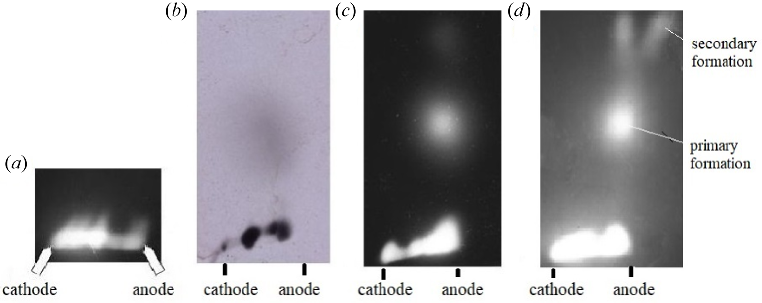
Turbulence in a plasma is created not only by plasma channels that appear as a result of the destruction of electrical domains, but also by fast particle fluxes. The stage of violation of the magnetic insulation in diodes is also accompanied by the appearance of fluxes of fast particles on the walls of the anode (Gorev et al. Reference Gorev, Dolgachev, Zakatov, Oreshko and Skoryupin1985). The mechanism of generation of fast particle fluxes can be explained on the basis of experiments on electrical breakdown near the surface of a dielectric. In the author's experiments on electric breakdown in air, it was found that in the head part of the current–plasma leader moving between the electrodes there is an electric domain with a strong field (Oreshko Reference Oreshko2006).
Frames of plasma glow during electrical breakdown near the dielectric surface, confirming the fact that the generation of fast particles occurs approximately perpendicular to the plane of the electric domain under the action of a transverse electromagnetic wave, are shown in figure 5. The frames were obtained using an electro-optical converter. The exposure in the frame was equal to 5 ns. The electric domain in the head part of the moving current–plasma channel periodically arises and collapses due to the ingress of neutral particles into it (see figure 5a). The frame in figure 5(d) is a very rare image in a series of experiments. This frame indicates that the generation of fast particles in discharges can have a two-stage character – first, a primary anomalous formation with a strong field appears in which an electrical breakdown occurs, which leads to the appearance of secondary fast particle flux and secondary formation.
Frames of plasma glow during electrical breakdown near the dielectric surface under the action of a transverse electromagnetic wave. Frame (b) is a positive image. The exposure in the frame was 5 ns.

Violation of plasma quasi-neutrality and the formation of electric domains in it with strong local fields are the main cause of turbulence. It should be noted that the generation of electric domains is accompanied by the appearance of strong electric and magnetic fields in their region and the appearance of microwave emission. It is the electrical domains and particle flows that are the real cause of plasma turbulence. The electrical domain is to some extent analogous to the elementary vibrator of the Nobel laureate G. Hertz. Experimental registration of microwave emission gives grounds to believe that transverse electromagnetic waves generated during nucleation of electric domains are the reason for the existence of particle fluxes. The dispersion equation for transverse electromagnetic waves which appear at the separation of charges in plasma has the form

The difference between expression (5.1) obtained in Oreshko (Reference Oreshko2006) and the expression given in Shafranov (Reference Shafranov1963) is in taking into account the conductivity of the plasma, which characterizes the continuity of the medium. Note that the original system of equations in Oreshko (Reference Oreshko2006) took into account the separation of charges under the action of electric and magnetic fields, while in Shafranov (Reference Shafranov1963) only the effect of the plasma density gradient was taken into account. The plane of the electric domain is perpendicular to the electric field strength and the field strength in the wave coincides with the strength of the external electric field. With the help of transverse electromagnetic waves, plasma ions and electrons are captured and accelerated into the region of the anode wall. The transverse electromagnetic waves generated in the discharge, which repeatedly interact with charged particles during their movement in the plasma, in fact perform the functions of multistage accelerators built into the plasma. It should also be noted that there is a significant difference between fast electrons accelerated by generated electromagnetic waves and runaway electrons from collisions. At a voltage of 8 kV, in experiments (Oreshko Reference Oreshko2006), particles accelerated by an electromagnetic wave with an energy of 80 keV were recorded. Electromagnetic waves generated during the birth of electric domains perform the functions of a multi-cascade accelerator in plasma. Enormous values of energy are gained by charged particles in vortex jets produced by electrical breakdown in giant electrical discharges between the tips of arms in spiral galaxies (Oreshko Reference Oreshko2023).
The magnetic field induction in a transverse electromagnetic wave significantly exceeds the magnetic field induction that is applied to the plasma by means of solenoids. Therefore, fast particles accelerated with the help of generated electromagnetic waves practically do not react to an external magnetic field.
6. Voltage resonance in the interaction of microwave radiation with the anode wall
It is impossible to deny the possibility of the influence of resonance on the pulse duration of the operation of the experimental set-up. Plasma is usually studied in metal chambers. Cylindrical metal chambers from the standpoint of radiophysics are hollow resonators (Kalinin & Gershtein Reference Kalinin and Gershtein1957). Therefore, plasma can be considered as an oscillatory system. The internal action in the system is provided by the continuously occurring charge separation in plasma, and the external one – with the help of a resonator. Communication between the elements of the system is provided with the help of electromagnetic waves generated during the separation of charges. The voltage resonance is realized when the cathode plasma approaches the anode. High-frequency voltage oscillations appear on the oscillogram of the voltage applied to the diode. Such oscillations are due to the appearance of a space charge in the plasma. The generation of electric domains in plasma generates transverse electromagnetic waves (Oreshko Reference Oreshko2006). The frequency of microwave radiation is 5–10 GHz, and the wavelength is commensurate with the diameter of the anode. Since the inner diameter of the coaxial anode is much smaller than the diameter of the chamber, when the cathode plasma enters the anode cavity, the quality factor of the resonator changes sharply. The transverse electromagnetic waves emerging from the plasma at the ‘plasma–vacuum’ interface become transmitted. The latter at the ‘vacuum–metal wall’ interface experience reflection. The amplitude of the reflected waves decreases. The waves reflected on the wall passing through the plasma will experience re-reflection on the opposite part of the resonator (anode). The re-reflected waves create waves in the same direction as the primary incident waves. The following cycles of re-reflection are similar, and the amplitude of their waves will be smaller due to energy losses. At some point in time, the incident and re-reflected incident waves in the resonator will have in-phase oscillations, the frequency of which is equal to the critical frequency of the resonator. Then the amplitude of the resulting incident wave will reach its maximum values. In this case, oscillations of the reflected waves will also add up in phase. Therefore resonance occurs in the oscillatory system. It follows that, in addition to the applied quasi-constant voltage component from the pulsed voltage generator, a microwave field is also applied to the plasma, which is established in the oscillatory system. The resulting value of the electric field strength in the plasma in the wave propagation region will be determined by the expression

Only in this way can one explain the presence of high-frequency oscillations on the oscillogram of the applied voltage, the amplitude value of which exceeds the value of the applied voltage (see figure 4c). When the critical value of the electric field strength is reached for the transition of electrons to the state of runaway from collisions, domains appear in the plasma, the nucleation of which is accompanied by the generation of electromagnetic radiation. A strong electric field, which is established in the plasma due to resonance, will contribute to the field mechanism of charge separation. In addition to the field, there is also a charge separation mechanism due to the plasma density.
7. The mechanism of violation of the plasma magnetic isolation
Electrical domains are generated in the plasma by means of runaway electrons. There is every reason to believe that the anomalous plasma diffusion across the longitudinal insulating magnetic field is also due to the appearance of electric domains in the plasma. A probable scenario of violation of magnetic insulation in a current-carrying magnetized plasma is as follows. In plasma, the redistribution of the current density occurs in a self-consistent way, as a result of which the current density becomes non-uniform in the cross-section, i.e. current flows through separate channels. The uneven current flow in a current-carrying plasma was discovered in the accelerator diode (Gorbulin et al. Reference Gorbulin, Zlotnikov, Kalinin, Skoryupin and Shashkov1982). This mode of current flow is energetically more advantageous than flowing current through a large-diameter plasma with the same current, because the inductance in the first case is less than in the second. It should also be noted that self-organizing current–plasma structures have been registered in high-current Z- and $\varTheta$ -pinch-type discharges (Kvartskhava et al. Reference Kvartskhava, Kervalidze, Gvaladze and Zukakishvili1965) and in a dense plasma focus (Gribkov et al. Reference Gribkov, Nikulin, Fadeev and Khodataev1993). It is known that in arc discharges the current passes through the main channel and the principle of minimum work (power) of Steenbeck (Reference Steenbeck1932) is fulfilled. According to this principle, at a given current strength in the plasma, the regime is realized at which the electric field strength becomes minimal. The minimum principle is a consequence of the well-known virial theorem. An increase in the current density in the channels leads to their heating and to the appearance of runaway electrons, with the help of which electric domains are generated. It is known also that the inductance of several parallel channels of small diameter with current is less than the inductance of one channel of large diameter. For this reason, a multidomain regime is sometimes realized in a plasma. Under the experimental conditions, three electrical domains were simultaneously observed in the plasma (see figure 2c). There are good reasons to believe that the direction of the electric field strength in the region of the domain is opposite to the direction of the field strength in the main part of the gap. Such a distribution of the field strength is energetically more favourable, since the work that is expended on the transition of a system of charged particles $A = q\boldsymbol{\nabla }\phi$
 from a state with a high potential value to a state with a low potential value is reduced. It should be noted that the field strength in the region of the streamer head is also directed against the field strength in the gap (Bazelyan & Raizer Reference Bazelyan and Raizer1998). In contrast to the streamer head, the generation of an electric domain is accompanied by the generation of a transverse electromagnetic wave. Depending on the RLC parameters of the electric circuit and the load in the plasma, one of four possible modes of domain generation is set (Oreshko Reference Oreshko2019a). In the mode with a delay in the appearance of domains, the interelectrode gap is bridged by electric domains, their subsequent destruction and the formation of plasma channels between the plasma and the wall (anode) (see figure 2e). Transverse electromagnetic waves in any case capture and accelerate charged particles to the chamber wall (see figure 4d,e). As plasma accumulates in the interelectrode space, its resistance decreases and the phase of electrical breakdown begins. In diodes, it leads to a sharp drop in voltage and an increase in current. The reason for the increase in current was explained earlier. Any of the electric domain generation modes leads to the fact that strong electric and magnetic fields are locally established in the plasma, which weaken the applied external magnetic field and lead to plasma ejection onto the chamber walls. In this case, the plasma passes into the anomalous diffusion mode across the longitudinal insulating magnetic field. In local regions of the plasma, there is a violation of the magnetic isolation. The speed of plasma movement in the radial direction under the action of the pressure gradient in magnetically insulated diodes increases by an order of magnitude.
Along with the field mechanism, separation of charges in the cathode plasma also occurs due to the inequality of the diffusion fluxes of electrons and ions across the longitudinal insulating magnetic field depending on the magnetic field induction. In weak fields, as is known, electrons diffuse more strongly; in strong fields, ions diffuse more strongly. The presence of the optimal value of the magnetic field induction ${\boldsymbol{B}_{opt}}$ in the sense of the maximum plasma confinement time (Bugaev et al. Reference Bugaev, Kim, Klimov and Koshelev1981) can be explained by the fact that, at a given value of induction, the ion and electron fluxes are close in magnitude at given values of the aspect ratio (the ratio of the cathode diameter to the anode diameter) that determines the level of uniformity of the density distribution plasma. The long pulse duration in reverse magnetically insulated diodes compared to direct diodes is associated with a longer time for establishing the critical value of the field strength for generating domains in the plasma, since with a comparable geometry of the electrodes of the direct and reverse diodes, the plasma density in the reverse diode is always lower than the density in a direct diode.
8. Conclusions
This article gives an explanation of the mechanism of anomalous plasma resistance and anomalous diffusion of magnetized plasma, as well as the appearance of fast particle flows on the basis of electrical domains found in plasma. Domain generation occurs due to runaway electrons, which in turn appear due to current channelling. In the process of generation, some of the plasma electrons pass into layers of excess negative charge of electric domains, and therefore the number of current carriers in the plasma decreases, and their speed also decreases. In the experiments, it was also found that the violation of the magnetic isolation of the plasma occurs due to the injection of electric domains from the plasma across the longitudinal magnetic field and the formation of plasma channels between the plasma and the walls of the experimental chamber. The passage of electric domains across the longitudinal magnetic field is due to the fact that, as a rule, they are quasi-neutral structures in whole and do not respond to the presence of a magnetic field. Thus, there is a violation of the transport barrier. The electric domain, as a quasi-neutral system as a whole, cannot be kept by either magnetic or electric fields. Attempts to keep high-energy ball lightning in the zone of its generation using an electric field did not give a positive result (Oreshko Reference Oreshko2015). It is possible that blobs and electrical domains have the same structure and generation mechanism. All complex processes have an elementary explanation, including irregular potential fluctuations, which form the basis of the theory of turbulent plasma convection. Irregular oscillations are due to the generation of electrical domains in plasma, in which the temperature and density change. Each subsequent electric domain in this case is born in a less dense and hotter plasma. The process is accompanied by a decrease in the critical value of the electric field strength, which contributes to the transition of electrons to the state of runaway from collisions and the emergence of new electric domains. The passage of an electric domain, which after its formation has a strong intrinsic electric field, does not make sense to interpret as the passage of an ion-acoustic soliton. A stable electric domain moving in a plasma with a strong electric field is an electrodynamic soliton. The domain instability found in experiments is a characteristic state that is realized in a magnetized current-carrying plasma due to the inequality of directed drift flows of ions and electrons, i.e. it is analogous to the two-stream Farley–Buneman instability (Buneman Reference Buneman1963; Farley Reference Farley1963). Since charged particles in Nature always tend to self-consistently move from a state with a high energy value to a state with a low value, it is necessary to develop fundamentally new methods that will really allow solving the energy problem.
All the best is in Nature and all processes occur in it in a highly rational way. Good results can be obtained by improving the accelerative mechanism of nuclear fusion, which takes place in the structural elements of the Sun (Oreshko Reference Oreshko2019b). The complete lack of financial support did not prevent the author of this work from obtaining ball lightning in the laboratory, which is a complete analogue of ball lightning observed in atmospheric electrical discharges in thunderstorm weather (Oreshko Reference Oreshko2007, Reference Oreshko2015, Reference Oreshko2021; Oreshko & Oreshko Reference Oreshko and Oreshko2021). It is possible that the use of ball lightning as a driver (Oreshko, Oreshko & Mavlyudov Reference Oreshko, Oreshko and Mavlyudov2018) or a reactor core will make it possible to solve the problem of obtaining nuclear fusion reactions.
Acknowledgements
The author thanks the anonymous referees for useful comments to the original manuscript, which contributed to the improvement of this article.
Editor Cary Forest thanks the referees for their advice in evaluating this article.
Funding
This research did not receive any specific grants or financial support from funding agencies in the state, commercial or non-profit sectors.
Declaration of interest
The author reports no conflict of interest.
Data access statement
The data that support findings in this study are available from the author upon reasonable request.