Introduction
In recent years, GaN has come to the forefront as a key material for next-generation, energy-efficient power electronics. Power devices based on the wide-bandgap semiconductor material GaN can convert power far more efficiently than Si-based chips, due to their higher critical electrical field (E c), faster switching speed, and lower on-resistance. At this moment, lateral GaN power devices are accepted as a breakthrough technology with disruptive performance. First demonstrators are available on the market from various suppliers, e.g., EPC, Panasonic, and GaN Systems. Most challenges for fabricating power devices on 200 mm GaN-on-Si substrates have been addressed such as device dispersion,[Reference Posthuma, You, Stoffels, Wellekens, Liang, Zhao and Decoutere1, Reference Posthuma, You, Stoffels, Wellekens, Liang, Zhao, De Jaeger, Geens, Ronchi, Decoutere, Moens, Banerjee, Ziad and Tack2] high-voltage operation,[Reference Posthuma, You, Stoffels, Wellekens, Liang, Zhao and Decoutere1, Reference Posthuma, You, Stoffels, Wellekens, Liang, Zhao, De Jaeger, Geens, Ronchi, Decoutere, Moens, Banerjee, Ziad and Tack2] e-mode operation,[Reference Posthuma, You, Stoffels, Wellekens, Liang, Zhao and Decoutere1, Reference Posthuma, You, Stoffels, Wellekens, Liang, Zhao, De Jaeger, Geens, Ronchi, Decoutere, Moens, Banerjee, Ziad and Tack2] and gate reliability.[Reference Stoffels, Bakeroot, Wu, Marcon, Posthuma, Decoutere, Tallarico and Fiegna3, Reference Rossetto, Meneghini, Canato, Barbato, Stoffels, Posthuma, Decoutere, Tallarico, Meneghesso and Zanoni4] One of the main challenges for the next-generation power devices is scaling the devices toward higher voltages and achieving a better reliability, enabling GaN to play a role in the important market of drive-trains.[Reference Kachi5] Another important challenge is a tighter co-integration of power devices on-chip, together with parts of the driver integrated circuit (IC). Typically, these components are integrated as discrete components and interconnected on a package level. This leads to additional parasitics, which particularly for a high power, fast switching technology as GaN can lead to excessive ringing and associated energy losses. Integrating several components on-chip, i.e., creating a GaN-IC will reduce circuit parasitics and cost. It is the key to unleash the full potential of the GaN technology.
Within this work, we evaluate and discuss new materials and substrate approaches which have potential to provide a (Al)GaN buffer with better crystal quality, higher critical electrical field, or thickness and have the potential to offer co-integration of GaN switches at different reference potentials, all this while maintaining lower wafer bow and maintaining complementary metal–oxide semiconductor (CMOS) compatibility. We have evaluated the merits both on the level of the material and also study the impact on reliability of GaN power devices fabricated on different substrates. The target diameter for the advanced substrates is 200 mm. We also evaluated GaN-on-SOI (silicon on insulator), combined with trench isolation as a key enabler for co-integration of GaN power switches.
In the next section, we will first discuss the different substrate materials. The different substrates have been compared by evaluating performance and reliability of 200 V rated buffers and p-GaN devices grown/fabricated on the different substrates. This benchmarking is discussed in “Device description” and “Comparison of device performance and reliability” sections. In “High-voltage devices” and “GaN-iC” sections we will specifically compare substrates and GaN buffers which exploit the specific advantages of the different substrate concepts, evaluating high-voltage GaN device technology on 200 mm and the application of GaN-on-SOI toward a GaN-IC.
Device description
The substrates which are compared in this paper are engineered silicon substrates with various doping levels and crystal orientations. SOI substrates with an oxide interlayer and finally coefficient of thermal expansion (CTE)-matched substrates which have been fabricated internally at imec and also commercially available QST® substrates with a CTE-matched core (details on the QST® substrates are given in Ref. Reference Steve6). More details on various substrates and initial characterization can be found in our previous publication.[Reference Stoffels, Geens, Zhao, Liang, Li, Van Hove and Decoutere7, Reference Geens, Van Hove, Li, Zhao, Šatka, Vincze and Decoutere8]
The device demonstrators were enhancement mode (E-mode) transistors with a p-GaN gate and were fabricated in a 200 mm CMOS compatible flow. Details on the fabrication flow can be found in Refs. Reference Posthuma, You, Stoffels, Wellekens, Liang, Zhao and Decoutere1, Reference Posthuma, You, Stoffels, Wellekens, Liang, Zhao, De Jaeger, Geens, Ronchi, Decoutere, Moens, Banerjee, Ziad and Tack2, and Reference Posthuma, You, Liang, Ronchi, Kang, Wellekens, Sarapalli and Decoutere9, while data on gate reliability has been published in Ref. Reference Stoffels, Bakeroot, Wu, Marcon, Posthuma, Decoutere, Tallarico and Fiegna3. A short summary shall be given here of the basic process steps.
The (Al)(Ga)N-based epitaxially grown layer has a total thickness of 3.3 µm and consists of an AlN nucleation layer, followed by a super lattice buffer layer for stress compensation, dispersion control, and for the blocking of the leakage current at high voltage.[Reference Stoffels, Zhao, Venegas, Kandaswamy, You, Novak, Saripalli, Van Hove and Decoutere10] The top layers consist of a carbon-doped GaN back-barrier, a GaN channel layer (300 nm), and an AlGaN barrier layer. A highly conductive two-dimensional electron gas (2DEG) is formed in the GaN channel due to the polarization differences in the channel and barrier layers. The final epitaxial layer is a p-GaN layer which has been optimized for achieving a high V t and low access resistance in the gate regions.[Reference Posthuma, You, Liang, Ronchi, Kang, Wellekens, Sarapalli and Decoutere9] The specific growth condition for the GaN buffer layer required some optimization depending on the substrate type, e.g., SOI substrates and CTE-matched substrates required some specific changes in nucleation and stress compensation layers to make sure that wafers were fully in spec for fabrication in a CMOS compatible pilot line. However, for each of these cases we have made sure that the final buffer was close in voltage ranges and that the active layer was grown under similar conditions.
As the gate metal TiN was used, which forms a Schottky contact toward the underlying p-GaN, the gate stack, consisting of the p-GaN, and gate metal have been processed using a self-aligned process.[Reference Posthuma, You, Stoffels, Wellekens, Liang, Zhao and Decoutere1] For the ohmic module, the passivation layers are opened, followed by an AlGaN barrier recess. Subsequently a Ti/Al-based metal stack is deposited and annealed to achieve the required ohmic behavior. The rest of the process consists of a metal[Reference Posthuma, You, Stoffels, Wellekens, Liang, Zhao and Decoutere1] interconnect layer and a power metal layer, both Al-based.
As a device demonstrator, a power bar with 36 mm total gate width was used, with a gate–drain distance of 6 µm, a gate length of 0.8 µm, and a source–gate distance of 0.75 µm. One gate field plate with a length of 1 µm was presented, as well as a two-level source field plate with respective lengths of 2 and 3 µm.
Comparison of device performance and reliability
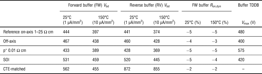
The different substrates have been compared with respect to performance and reliability on both buffer level and device level. For the buffers, the vertical breakdown, buffer-induced dynamic on-resistance (R on,dyn), and time-dependent dielectric breakdown (TDDB) of the buffer have been measured. Results of the comparison are summarized in Table I.
Comparison of buffer performance and reliability for different substrates.

The vertical breakdown voltage (V bd) of the buffer layer is measured on an isolation structure, which is a 100 µm × 100 µm active island with contact metallization on top. The value for V bd is defined at a current criterium of 1 µA/mm2 at 25°C and 10 µA/mm2 at 150°C. Leakage curves have been measured at forward and reverse polarization and this at 25°C and 150°C. For the engineered silicon concepts, no significant difference could be observed for the rated voltage, when evaluated at 1 µA/mm2. As has been shown in Ref. Reference Steve6, there is still a voltage plateau for the lowly p-doped substrates just above our current criterium. For the SOI substrate a difference of about 100 V in the V bd was observed, which is caused by a difference in stress compensation layers when compared with the reference buffer. The total buffer thickness of the 200 V buffer on SOI was 3.7 µm, while the reference buffer was 3.2 µm. A more important difference could be noted for the (Al)(Ga)N buffers on the QST® substrates, which had a similar thickness compared with the SOI buffer, but substantial differences in V bd. For the buffers on the QST® substrates the V bd under reverse polarization was increased about 400 V, when compared with the reference and SOI buffers. The difference could be either due to the silicon layer taking up part of the voltage or alternatively an increased critical field of the (Al)(Ga)N buffer. The superlattice (SL) part of the (Al)(Ga)N buffer, grown on the QST® substrate, contained a higher percentage of AlN. Growing such a layer was enabled by the CTE-matched properties of the QST® substrate, whereas the growth of a similar layer on Si leads to excessive cracks in the wafer. It is known that AlN has a 3–4× higher critical electrical field compared with GaN.[Reference Kamata, Ishii, Mabuchi, Naoe, Ajimura and Sanada11] This could potentially explain the difference in V bd under reverse polarization, however more investigation would be needed to confirm this hypothesis and to understand the exact transport dynamics through these buffers.
To evaluate the R on,dyn induced by the buffer on the 2DEG, a measurement methodology, using a 2DEG resistor is used.[Reference Stoffels, Zhao, Venegas, Kandaswamy, You, Novak, Saripalli, Van Hove and Decoutere10] Two distinct steps were used in the measurement procedure, namely a stress and a recovery phase. During the stress, a potential is applied on the substrate (V bulk = V stress), while the contacts of the 2DEG resistor are biased at ground potential. During the recovery, the variation of the resistance (R tlm) over time is recorded by applying a small sensing voltage over the 2DEG resistor (V tlm = 1 V). This allows us to define a value for the R on,dyn induced by the buffer, by calculating the ratio of the initial 2DEG resistance of an unstressed device to the values measured after stress (ΔR on = R tlm/R init). No significant differences could be observed in the buffer-induced R on,dyn, i.e., all values were similar to the reference condition, having a ΔR on around −5%.
The final parameter which has been compared on the buffer level is the TDDB of the buffer. In previous publication[Reference Borga, Meneghini, Rossetto, Stoffels, Posthuma, Van Hove, Marcon, Decoutere, Meneghesso and Zanoni12] it has been demonstrated that a GaN buffer is subject to a time-dependent degradation. Lifetime extrapolation and derivation of maximum applicable voltage can be done through constant voltage stress and Weibull statistics. For this work V max was determined by scaling the active area to 0.9 mm2, lifetime to 10 years, and failures to 0.1%, the procedures are demonstrated in Ref. Reference Borga, Meneghini, Rossetto, Stoffels, Posthuma, Van Hove, Marcon, Decoutere, Meneghesso and Zanoni12. A first important observation is that the buffers have a significant margin for reaching the 200 V specification. The V max for the buffers on the different substrates is in line with only the p+ substrates having an apparent higher lifetime. This aberrant behavior is caused by a transition of leakage mechanism on this particular buffer around the applied stressing voltage, this causes a mixing of degradation/leakage mechanisms and does not allow to perform an accurate extraction of the lifetime. Applying a lower bias voltage, to avoid the transition of leakage mechanism would lead to unrealistically long stressing times and was not pursuit. The transition of the leakage mechanism could potentially be caused by an avalanching in the silicon substrate, which happens at lower voltage for a p+-doped Si substrate. However, an additional investigation would be needed to corroborate this statement.
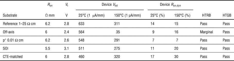
In a second step the different substrates have been compared at the device level by fabricating 200 V e-mode p-GaN device demonstrators and evaluating performance and reliability of these demonstrators (see “Device description” section). The device breakdown, device R on,dyn, high-temperature reverse bias (HTRB), and high-temperature gate bias (HTGB) of the devices has been measured and results compared in Table II.
Comparison of device performance and reliability for different substrates.

For the device breakdown the devices are biased in the off-state with 0 V V g, the V ds is swept from 0 V to hard breakdown. V bd is extracted at 1 µA/mm for both 25°C and 150°C. It can be seen that also for the case of the device breakdown a significant margin is achieved for 200 V device operation at room temperature, and a slight margin at 150°C. For the reference substrate a slightly higher V bd is achieved at 25°C, this is because a plateau is present on these devices which is just below 1 µA/mm, causing a positive shift of around 100 V for the breakdown. The off-axis wafers on the other miss the leakage specification at 150°C, which is caused by the increased 2DEG concentration (n s) on these substrates as we have demonstrated in earlier work.[Reference Steve6] The higher n s causes the threshold voltage (V t) to shift slightly negative and causes an increase in the subthreshold leakage. This was evaluated on the transistor level where we observed a 600 mV negative shift in the V t for the off-axis cut wafers compared with the reference condition. The subthreshold leakage for the off-axis devices increased both at 25°C and 150°C compared with equivalent devices fabricated on the reference substrate, however at room temperature the subthreshold leakage was still below our current criterium of 1 µA/mm, while at 150°C is passed it, explaining the drop in V bd at 150°C. For this concept the barrier and p-GaN condition needs to be tuned in to bring device performance in-line with the reference condition, this could be beneficial as e.g., a lower Al% can be used in the barrier to achieve a similar n s which can help device reliability as demonstrated for RF devices.[Reference Marcon, Viaene, Favia, Bender, Kang, Lenci, Stoffels and Decoutere13]
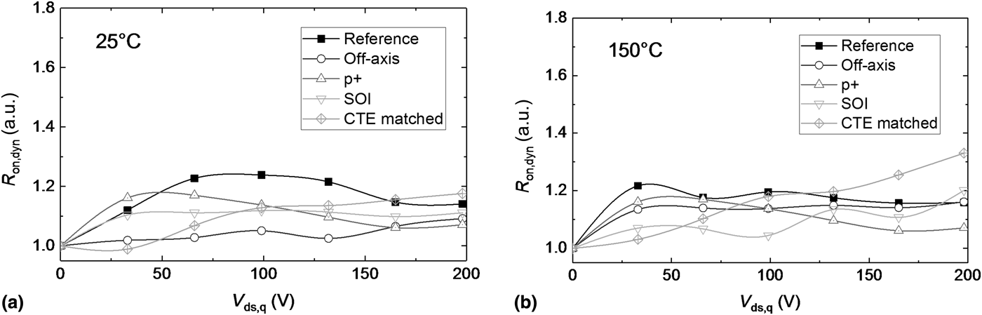
Another important device parameter is the dynamic on-resistance (R on,dyn) of the p-GaN HEMT power transistor and is typically assessed by double-pulsed IV measurements. In a double-pulsed measurement, both drain and gate are synchronously pulsed from a constant off-state bias condition (quiescent bias) to the on-state bias condition (non-quiescent bias). The device technology has been optimized for low R on,dyn with the reference process typically achieving values of device dispersion below 20%. From the curves in Fig. 1 and the comparison in Table II, it can be seen that the type of substrate only had a limited impact on the R ds-on,dyn, with all values staying below 20–30%. There are some differences in the response of the R on,dyn versus voltage, e.g., for the CTE-matched substrates the R on,dyn tends to initially increase slower compared with buffers on other substrates and only increase at higher voltages. These differences could be due to the particular buffer optimization for each of the substrates.
Comparison of the R on,dyn for 200 V p-GaN devices fabricated on different type of substrates, measured at (a) 25°C and (b) 150°C.

Finally, device stability has been evaluated by performing on-wafer HTRB and HTGB, for 10k at 150°C. The reverse bias was performed at 100% of the rated voltage (i.e., 200 V) and the gate bias at V g = 6 V. There was no change in device stability with respect to the different substrate concepts. Only for the off-axis cut wafers the wafer were only marginal under HTRB testing due to the increased subthreshold leakage. This indicates that there is no impact on short-term device stability and/or early failures. A more rigorous analysis would be needed as part of package level product qualification to distinguish differences in long-term device reliability between the substrates, however such exercise was outside of the scope of this work.
High-voltage devices
Based on the results presented in “Comparison of device performance and reliability” section and Ref. Reference Steve6, we will investigate the different substrate concepts and exploit there intrinsic strength to evaluate a path toward high-voltage GaN technology on a 200 mm CMOS compatible processing line. High-voltage GaN-on-Si wafers have been demonstrated,[Reference Christy, Egawa, Yano, Tokunaga, Shimamura, Yamaoka, Ubukata, Tabuchi and Matsumoto14–Reference Boutros, Burnham, Shinohara, Hughes, Zehnder and McGuire17] however these publications either had demonstrations on small wafer sizes or did not demonstrate aspects needed for introducing wafer is a CMOS compatible production fab. In this section, we will discuss how the substrate can be scaled up in voltage, by exploiting new substrate concepts, in the context of 200 mm CMOS compatible processing.
A first observation is that for the engineered silicon substrates, with low p-type doping, a plateau region is presented in the devices,[Reference Steve6] which could be used to extend the voltage range of the components. However, a thorough understanding of the transport physics and reliability in this region is needed before being able to ascertain if a device is amendable for operation in this regime. In Refs. Reference Li, Van Hove, Zhao, Bakeroot, You, Groeseneken and Decoutere18 and Reference Borga, Meneghini, Stoffels, Li, Posthuma, Van Hove, Decoutere, Meneghesso and Zanoni19, we have investigated the transport physics and impact on the reliability of the components in more detail for each of these regimes. The most important conclusions of these publications are that a plateau in the leakage occurs, originating from the partial depletion of the p− substrate; once depletion starts, the field stops increasing on the AlN, and starts dropping on the substrate. As a consequence, the probability of tunneling through the triangular barrier at the Si/AlN interface remains unchanged, and leakage current stops increasing. For higher voltages, gradually avalanching starts occurring in the Si depletion layer, at which point the electrical field over the AlN and the leakage current increases once again. It was also revealed in Ref. Reference Borga, Meneghini, Stoffels, Li, Posthuma, Van Hove, Decoutere, Meneghesso and Zanoni19 that the presence of the plateau in the leakage current causes additional device degradation when the device off-state bias voltage is above the on-set of the plateau. This degradation happens due to a temporary positive buffer-to-drain bias when switching from off-state to on-state. As revealed in Refs. Reference Stoffels, Zhao, Venegas, Kandaswamy, You, Novak, Saripalli, Van Hove and Decoutere10 and Reference Borga, Meneghini, Stoffels, Li, Posthuma, Van Hove, Decoutere, Meneghesso and Zanoni19, a positive buffer-to-drain bias causes a significant increase in buffer trapping and related R on,dyn increase. Therefore, even though lowly doped silicon substrate can significantly extend the voltage range of the devices it leads to additional unwanted device instability and is thus not a feasible mechanism to extend the voltage range of the components. One potential path to mitigate these issues could be to reoptimize the GaN buffer topology and in particular the back-barrier, as demonstrated in Ref. Reference Freedsman, Egawa, Yamaoka, Yano, Ubukata, Tabuchi and Matsumoto15 as this can eliminate dispersion under negative bulk bias, this however carries an additional penalty as it reduced the critical electrical field (E c) of the buffer.
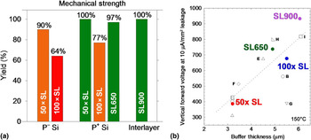
Another important aspect is the mechanical stability of the substrates. Marcon et al.[Reference Marcon, Saripalli and Decoutere20] have highlighted the importance of reproducible, high quality, and defect-free GaN epitaxy for processing in a CMOS compatible fab. Additionally, wafers need to have a wafer warp within a tolerance of ±50 µm over the wafer, which is needed for automatic handling of the wafers and to ensure tool compatibility. To scale up the voltage range of the component, a thicker GaN buffer needs to be grown, which leads to additional defects and cracking of the layer, as explained in Ref. Reference Marcon, Saripalli and Decoutere20. These defects can cause wafer breakage during processing and is a critical issue for processing in an automated CMOS-compatible fab. Therefore, a mechanical screening is performed to eliminate weak wafers from the process, which would otherwise break during processing. Wafers which are highly boron-doped can help to increase the mechanical rigidity of the GaN-on-Si wafers.[Reference Steve6] A further confirmation has been done by growing different GaN buffer architectures on the different substrate concepts and sending them through the mechanical screening procedure. The mechanical yield is defined as the percentage of wafers which pass the screening procedure without breaking. The results from the mechanical screening [Fig. 2(a)] show a 13% point increase in yield for p+ Si substrates, compared with a similar GaN buffer grown on p− Si substrates. A 100× SL has e.g., 65% yield on p− substrates, while the same stack on p+ gives a yield of 77%. A further increase in yield on p+ is possible by increasing the E c of the buffer, as demonstrated by the SL650 buffer, which from Fig. 2(b) is thinner, but has a higher vertical forward breakdown voltage. This SL650 buffer has a yield of 97% after mechanical screening, which is sufficiently high for a 650 V rated GaN platform. There are however still limitations in maximum achievable buffer thickness, even for the p+ substrates, as can be noted by the decreased yield for the 100× SL. The GaN-on-SOI, using a specially developed buffer architecture, allows to overcome this limitation and 900 V-rated buffers [Fig. 2(b)] could be demonstrated with a high yield [Fig. 2(a)]. The statistics for SL900 wafer is still limited but it demonstrates the potential of these substrates for reaching a high-voltage (≥900 V) 200 mm GaN platform.
High-voltage GaN buffers on 200 mm substrates in a CMOS compatible fab. (a) Mechanical yield for different substrate types and buffer topologies and (b) breakdown voltage versus buffer thickness, measured at 150°C, for several of the key GaN buffers.

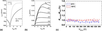
A 650 V platform has been developed on the p+ substrates to demonstrate the capabilities of the technology and the selected substrate type. Details on the fabrication and stability of the developed platform can be found in Refs. Reference Posthuma, You, Stoffels, Wellekens, Liang, Zhao and Decoutere1–Reference Stoffels, Bakeroot, Wu, Marcon, Posthuma, Decoutere, Tallarico and Fiegna3. The devices measured were 36 mm power bars with a V t of 2.1 V [Fig. 3(a)], an R on around 15 Ω mm [Fig. 3(b)], and an R on,dyn which is stable over the entire off-state bias range [Fig. 3(c)].
Characteristics of 650 V power transistors fabricated on p+ substrates: (a) subthreshold characteristics, (b) I dV d, (c) device R on,dyn versus off-state voltage and for 25°C/150°C, 90 µs off-state, 10 µs on-state.

A further increase in achievable buffer thickness (and thus breakdown voltage) can be achieved by using CTE-matched substrates. For silicon substrates the main limitation is growing thick uninterrupted GaN layers. The CTE-matched QST® substrates offer a breakthrough in the growth of very thick GaN layers. Hydride vapor phase epitaxy (HVPE) grown GaN layers with thicknesses in the range of 10–100 µm have already been obtained.[Reference Leach, Udwary, Quayle, Odnoblyudov, Basceri, Aktas, Splawn and Evans21] We have demonstrated a metalorganic vapor phase epitaxy (MOCVD) grown GaN stack on QST® substrates, with a total thickness of 18 µm.[Reference Stoffels, Geens, Poshtuma, Zhao, Liang, Li, Wellekens, You, Bakeroot, Van Hove and Decoutere22] This is sufficient to reach a theoretical breakdown voltage of ~2.5 kV and offers an interesting avenue to enable fabrication of high-voltage GaN devices on large-area substrates. First demonstrators have been fabricated on 6 in. substrates and show capabilities to grow buffer thicknesses far beyond the current state of the art of similar stacks on GaN-on-Si,[Reference Khadar, Liu, Zhang, Xiang, Cheng and Matioli23–Reference Zhu, Song, Qi, Hu, Nomoto, Yan, Cao, Johnson, Kohn, Jena and Xing25] which have a maximum thickness of around 6 µm. Moreover, the technology on CTE-matched substrates has the potential to scale such thick stacks up to 8 in. (and beyond).
GaN-iC
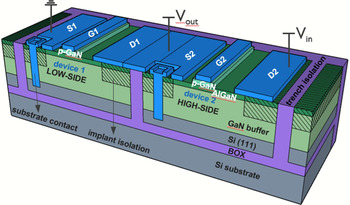
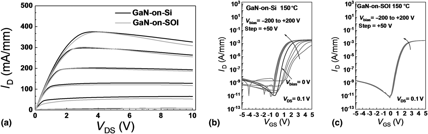
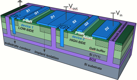
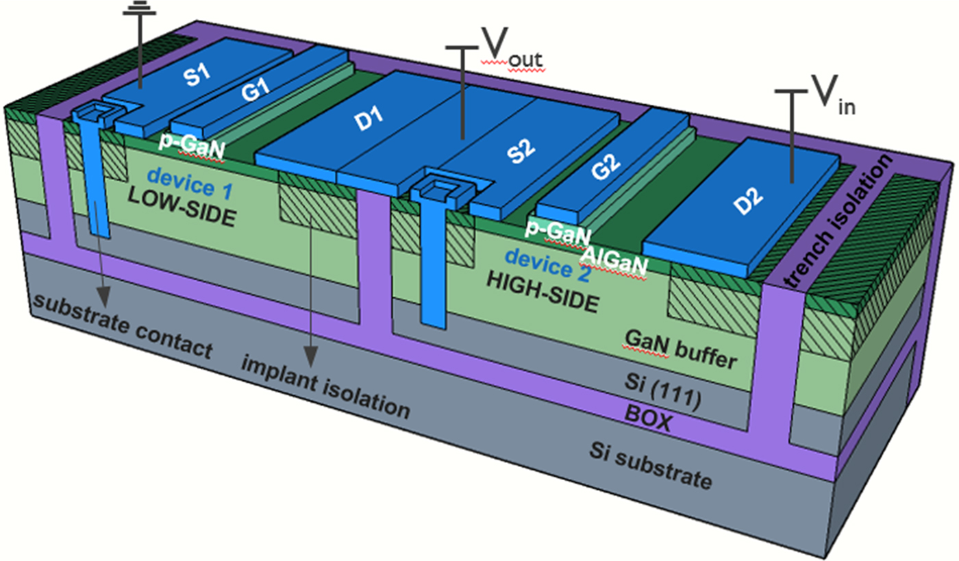
Using silicon as a substrate has the disadvantage that it does not allow lateral isolation between two power devices with different source voltage. A source to bulk contact is needed to provide proper referencing for the substrate. This however hinders the co-integration of high-side and low-side switches on a single chip. Epitaxial growth of GaN-on-SOI, combined with trench isolation allows to reference each transistor to its own “bulk island” through a substrate contact, allowing for integration of switches on a single chip (GaN-iC). The concept was detailed in our earlier publication by Li et al.[Reference Li, Van Hove, Zhao, Geens, Lempinen, Sormunen, Groeseneken and Decoutere26] A schematic cross-section of the concept is shown in Fig. 4. To validate the concept, 200 V power transistors, with a total gate width of 36 mm, have been fabricated in this platform and benchmarked with respect to regular GaN-on-Si wafers by comparing device characteristics. The transistors have also been evaluated in a “half-bridge” configuration, comparing characteristics of GaN-on-Si transistors, for different applied bulk bias, with a GaN-on-SOI transistor where the bulk bias was applied to a neighboring island. Results are shown in Fig. 5, clearly indicating that for the GaN-on-SOI transistors, the characteristics are stable and that transistors configured in a half-bridge configuration, designed in this platform do not affect each other's behavior, while significant instability can be observed for similar power transistors fabricated on a GaN-on-Si platform.
Schematic representation of an on-chip half-bridge realized on a GaN-on-SOI substrate.
Comparison of device characteristics of a 36 mm power bar for GaN-on-SOI with trench isolation and regular GaN-on-Si for (a) I dV d, (b) I dV g versus bulk bias for GaN-on-Si wafers and (c) I dV g for GaN-on-SOI wafers with trench isolation. The bias reference is applied to a neighboring island.

Conclusions
In this work, we highlighted main advances on novel substrates for epitaxial (Al)(Ga)N growth and evaluated reliability of large power bars fabricated on these different substrates. The advantage and reliability is also discussed in the context of new applications which are enabled by these substrates, such as high-voltage devices and GaN-iC type of applications. The substrates which have been considered are engineered Si substrates with either a modification in the doping level or crystal orientation, SOI wafers (oxide interlayer), and CTE-matched substrates.
A reliability benchmarking has been performed by fabricating 200 V p-GaN e-mode HEMT devices on the varying substrates and this in the substrate and device levels. It was found that device performance was not significantly impacted by the substrate type. Only for the CTE-matched substrate, a significant improvement was observed in the V bd under reverse biasing of the substrate potential, moreover an almost complete absence of buffer-induced R on,dyn has been observed. Reliability, performance and stability of the devices were found to be in-line for all substrate types.
In the context of high-voltage devices, it was shown that engineered p+ Si substrates and interlayer substrates are shown to offer significant advantages to reach high-voltage operation while maintaining high mechanical yield. The p+ Si substrates offer an evolutionary path and a 650 V p-GaN e-mode HEMT platform has been demonstrated on these substrates in a 200 mm CMOS pilot line, achieving high yield during wafer processing (i.e., low-wafer breakage). SOI wafers on the other hand were shown to offer a path toward 900 V or higher voltage ranges, with a buffer demonstrated which could pass mechanical screening with high yield and having high V bd of 900 V (for a 200 mm wafer size). CTE-matched substrates, finally offer breakthrough performance in achievable buffer thickness, showing uninterrupted GaN growth in a stack with 10 µm drift region, while state-of-the-art GaN-on-Si buffers have not been reported above 4 µm drift region thickness.
A path toward a GaN-iC has also been demonstrated, opening possibilities for a power system on chip. GaN-on-SOI, combined with trench isolation was shown to offer on-chip isolation of high- and low-side switches. Power transistors have been fabricated to demonstrate the capability, showing device performance for GaN-on-SOI which is in-line with our reference platform on GaN-on-Si, however not suffering from back-biasing.
Acknowledgments
Part of this work has been performed under collaboration between imec, QROMIS (Santa Clara, California, USA), and Aixtron (Aachen, Germany).