Key power-switch requirements and the limitations of silicon devices
The generation, transmission, and use of electric power require different forms of power conversion. The following are illustrative examples: The AC main power must be converted into DC power to run consumer electronics many electronic circuits require DC-to-DC conversion from one voltage level to another, and DC power from solar cells needs to be converted into AC power to be connected to electrical appliances or to the power grid. The commonly used electronic circuits for power conversion utilize switching techniques and, consequently, are referred to as switch-mode power electronic circuits. Two types of semiconductor-based switches are used in these circuits: two-terminal rectifiers (diodes) and three-terminal controlled switches (transistors). Three key power-switch requirements are common for both diodes and transistors: (1) high-blocking voltage, (2) high-power efficiency, and (3) high-switching speed. The fourth key requirement is specific to the controlled switches and relates to a strong preference for normally OFF switches—switches that are OFF when no controlled voltage is applied and are turned ON by a positive controlled voltage.
High-blocking voltage
The blocking voltage is the voltage that can be applied across a switch in OFF mode, which is the reverse-bias voltage that can be applied either across a diode or a transistor. The maximum achievable blocking voltage corresponds to the breakdown voltage of a planar structure (no corners) and to the lowest possible doping concentration of the semiconductor region supporting the electric field due to the reverse bias. In the case of Si and SiC, this region is n-type doped and referred to as the drift region. For a planar structure, the relationship between the breakdown voltage and the critical field that leads to breakdown can be obtained by solving the one-dimensional Poisson equation:Reference Dimitrijev1
 $$V_B = {{\varepsilon _s E_{cr} } \over {2qN_D }}^2 $$
In Equation 1, V B is the breakdown voltage, E cr is the critical or breakdown electric field, N D is the n-type doping level, εs is the semiconductor permittivity, and q is the value of electron charge.
The critical field of Si, which is about E cr = 3 × 10⁵ V/cm (30 V/µm), is the limiting factor for many applications. Assuming the lowest possible doping of N D = 1014 cm–3, the highest achievable breakdown voltage is just over 2900 V (εs = 11.8 × 8.85 × 10−12 F/m). For N D = 5 × 1014 cm–3, the breakdown voltage drops below 600 V. The critical field relates to the strength of the atomic bonds, which is further related to the energy gap of the material (1.12 eV in Si). The wider energy gaps in SiC and GaN (3.2–3.4 eV) correspond to stronger atomic bonds and 10 times higher critical field (E cr = 300 V/μm in SiC). This means that the maximum breakdown voltage at N D = 5 × 1014 cm–3 is close to 50,000 V (εs = 10 × 8.85 × 10–12 F/m).
Based on these values of breakdown voltages, it is clear that Si-based power electronics are suitable for applications below 600 V, which can be classified as power management in information technology and consumer electronics. Applications requiring blocking voltages higher than 600 V, which can be classified as switching applications, include (1) automotive applications (DC/DC and DC/AC converters for electric vehicles and hybrid electric vehicles), (2) inverters for industrial applications, such as photovoltaic energy supply, motor drives, and uninterrupted power supplies, and (3) inverters for DC transmission of electric energy.Reference Rabkowski, Peftitsis and Nee2–Reference Biela, Schweizer, Waffler and Kolar4 The switching applications can only be achieved by materials with wider energy gaps than Si, specifically SiC and GaN.
High-power efficiency
The requirement for high-power efficiency, which should be as close as possible to 100%, is the main reason for the use of switching circuits for power conversion. Power losses during the conversion can be classified as static and dynamic.Reference Lidow, Strydom, de Rooij and Reusch5 The dynamic losses are due to charging and discharging of parasitic capacitances (C) during switching: P dynamic= fCV CReference Rabkowski, Peftitsis and Nee2, where f is the switching frequency and V C is the voltage that the parasitic capacitance (C) is charged to. In the case of transistors, the parasitic capacitances can be considered as the equivalent input (C in) and the equivalent output (C out) capacitances. The equivalent input capacitance is usually higher, and it may dominate the dynamic power loss in low-voltage applications. However, the dynamic power loss due to the output capacitance will dominate and can be very large when these capacitances are charged to very high voltages in high-voltage applications. Note that the power loss is proportional to V BReference Rabkowski, Peftitsis and Nee2 in that case,
 $$P_{dynamic} = fC_{out} V_B ^2 ,$$
assuming that the output voltage reaches the breakdown voltage V B.
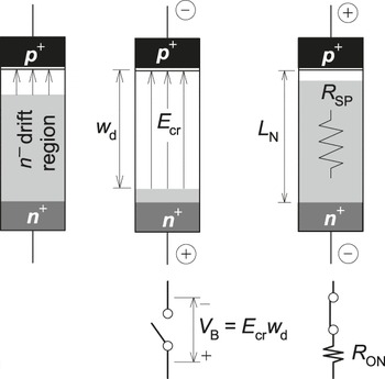
The static losses are due to non-zero voltages (V) when the switches conduct current (I) in ON mode (P static= VI). In the case of both diodes and transistors, the main source of static power losses is the resistance of the low doped (n –) drift region, which is necessary for achieving high-blocking voltages (Figure 1).Reference Dimitrijev1 The illustration in Figure 1 is for the case of a p–n junction diode; however, the same concept applies to transistors and Schottky diodes. As can be seen, the length of the drift region (L N) should not be smaller than the width of the depletion layer (w d) when the maximum reverse-bias voltage, which is the breakdown voltage, is applied:
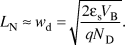 $$L_N \approx w_d = \sqrt {{{2\varepsilon _s V_B } \over {qN_D }}} .$$
Illustration of the role of the drift region in power rectifiers/switches and the relationship between the specific ON resistance (R SP) and the maximum achievable breakdown voltage (V B).Reference Dimitrijev1 (Left) The first schematic is for an unbiased p–n junction, whereas (middle) the second and (right) third schematics correspond to reverse-biased and forward-biased p–n junctions, respectively. The second schematic for the reverse-biased p–n junction (switch in OFF mode) shows that the reverse-bias voltage depletes the n – drift region, and the depletion-layer width (w d) and the maximum electric field (E cr) determines the maximum voltage that can be applied (V B). The third schematic shows that the n – drift region introduces a series resistance when the p–n junction is forward biased (the resistor R ON in series with the switch in ON mode). Note: E cr, critical, or breakdown, electric field; L N, length of the drift region; R ON, ON resistance. Adapted from Reference 1.

Therefore, a higher blocking voltage requires a wider depletion layer, which results in a longer drift-region resistor when the device is turned ON. Defining specific ON resistance of the drift region as the ON resistance for a given area,
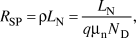 $$R_{SP} = \rho L_N = {{L_N } \over {q\mu _n N_D }},$$
where ρ is the resistivity of the material, and the following relationship is obtained between the specific ON resistance and the blocking voltage:
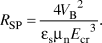 $$R_{SP} = {{4V_B ^2 } \over {\varepsilon _s \mu _n E_{cr} ^3 }}.$$
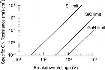
In Equations 4 and 5, μn is the mobility of electrons in the drift region. This relationship between the specific ON resistance and the breakdown voltage, which determines the maximum blocking voltage by the drift region, is illustrated in Figure 2. Based on the plot for Si, we can demonstrate the severe limit imposed by the relatively low breakdown electric field of Si. Assuming that a switch has to conduct 10 A of current in the ON mode and the active area of the device is 1 cm2, for the specific resistance of 100 mΩ⋅cm2, which corresponds to a blocking voltage of 1000 V, the ON resistance of this device will be 0.1 Ω. For a 10 A current, 1 V drops across the drift region, which corresponds to 10 W of power loss. This analysis shows that the critical electric field limits the practical blocking voltages that can be achieved by silicon devices to values below 1000 V.
The relationship between the specific ON resistance of the drift region and the maximum achievable breakdown voltage for three different materials. These plots correspond to Equation 5 and the parameter values specified in the text. The plotted results show that, for a given specific ON resistance, the corresponding breakdown voltage is 10 times higher in SiC in comparison to Si, and even higher in the case of GaN. Reprinted with permission from Reference 6. © 2014 IEEE.

The analysis that leads to Equation 4 and the results plotted in Figure 2 are for a planar structure and a homogeneous n-type doped drift region. The electric field in this structure is increasing from its zero value at the edge of the depletion region to its maximum value at the top edge of the drift region (the junction in diodes or the surface in metal oxide semiconductor field-effect transistors [MOSFETs]). It is possible to increase the field toward the edge of the depletion layer by creating p-type columns inside the drift region. The resulting effect is an increase in the voltage that can be supported by a drift region with the same doping and the same length. In effect, the created p–n junctions between the p-type columns and the n-type drift region are reverse biased, and the negative charge from the depleted p-type areas is reducing the electric field at the surface. In the ON mode, the purpose of these columns is to reduce the active area of the drift region. However, the increase in resistance due to the reduction of the active area is smaller than the reduction of resistance due to the possibility to increase the doping level of the drift region, which is enabled by the screening effect of the p-type columns. This approach can be applied to both diodes and MOSFETs to increase the blocking voltage, for a given specific resistance, above the theoretical limit for the planar structures. When this approach is applied to MOSFETs, the resulting device is referred to as CoolMOS.Reference Deboy, März, Stengl, Strack, Tihanyi and Weber7–Reference Lorenz, Deboy, Knapp and Miirz9
High-switching speed
High-switching speed enables the use of smaller inductors and transformers, which can significantly reduce the size and cost of power systems. The size reduction is important because it enables applications that otherwise would not be possible. This requirement sets a very strong preference for unipolar devices to avoid long switching delays due to the need to recombine accumulated minority carriers.
In the case of diodes, this means a very strong preference for the unipolar Schottky diodes over the bipolar p–n junction diodes. However, the practical barrier heights in Si-based Schottky diodes are very low and limit the practical blocking voltages to hundreds of volts—too low for most practical applications.
In the case of transistors, this means a disadvantage for bipolar junction transistors and a strong preference for the unipolar transistor, in particular MOSFETs.
Normally OFF operation of controlled switch
The third key requirement is a normally OFF controlled switch. This means that the switch is in OFF mode when no voltage is applied at the controlling electrode (gate), and it is set in ON mode by an above-threshold positive voltage at the transistor gate. The only device structure that could enable achievement of this requirement is the MOSFET.Reference Dimitrijev1 This is such a fundamental requirement for both power-switching applications and digital electronics that it is the primary reason for the MOSFET dominance among semiconductor devices and complementary MOSFET (CMOS) technology for digital electronics.
Commercial availability of SiC switches
Based on the analysis in the previous section, it is obvious that a semiconductor material that can withstand higher electric fields is necessary to enable blocking voltages above 1000 V. It was realized in the late 1980s and early 1990s that SiC could enable the development of superior power switches.Reference Baliga10–Reference Ferry13 The breakdown electric field for SiC was estimated to be 300 V/μm,Reference Ferry13 almost 10 times higher than the breakdown field of Si (about 30 V/μm). As illustrated in Figure 2, the same specific ON resistance of 100 mΩ⋅cm2 corresponds to a maximum blocking voltage of 10,000 V. In addition to the very high breakdown field, it was found that Schottky diodes with a sufficient barrier and very high breakdown voltage could be created with SiC. Furthermore, the thermal conductivity of SiC (3.5 W/cm°C) is more than two to three times higher in comparison to Si (1.5 W/cm°C),Reference Shenai, Scott and Baliga11 which enables better heat conduction away from the power switch. Additionally, SiC Schottky diodes could operate at much higher temperatures than Si.
As a result, Cree commercialized SiC Schottky diodes, and they are now available from Infineon, Rohm, and other suppliers. The cost of SiC Schottky diodes was initially high, and it is still relatively high in comparison to Si p–n junction diodes; however, the fast switching enabled by the SiC Schottky diodes allows for fabrication of cheaper, smaller, and more efficient power systems. For applications that require blocking voltages of up to 1700 V, SiC Schottky diodes are by far the best choice, and their adoption by system designers will continue to grow.
In addition to Schottky diodes, SiC provided the promise of normally OFF MOSFETs—the preferred controlled switch for power-electronic systems. Before SiC, commercial MOSFETs were formed only with Si, because sufficient electronic passivation of dangling bonds at the semiconductor surface could only be achieved by thermally grown SiO2 as the gate dielectric. The fact that thermal oxidation of SiC also creates SiO2 was a significant motivating factor to attempt the development of MOSFETs in SiC. Cree led the development—demonstrating the first vertical SiC MOSFET device, the first SiC MOSFETs at >600 V, and the highest voltage MOSFETs ever fabricated (10 kV)Reference Cheng, Palmour, Agarwal, Allen, Brunt, Wang, Pala, Sung, Huang, O’Loughlin, Burk, Grider and Scozzie14—although with critical contributions made by many research institutions.
Numerous problems were solved, but one significant problem persisted for a long time: electronic passivation of the SiC–SiO2 interface, created by either dry or wet oxidation of SiC, remained insufficient because the electrons attracted to the surface of SiC by the gate voltage would be trapped by a very high density of active defects at the interface. Hydrogen annealing and passivation were effective at the Si–SiO2 interface but did not work in the case of the SiC–SiO2 interface. The presence of carbon resulted in a sufficiently different material system, and a new approach was necessary. A breakthrough was eventually made by nitriding the SiC–SiO2 interface, either grown or annealed in an NO atmosphere at temperatures above 1000°C. Researchers from Griffith UniversityReference Li, Dimitrijev, Harrison and Sweatman15,Reference Dimitrijev, Harrison, Tanner, Cheong, Han, Choyke, Matsunami and Pensl16 initiated and published this process, which resulted in acceptable mobility of electrons in the MOSFET channel.Reference Chung, Tin, Williams, McDonald, Chanana, Weller, Pantelides, Feldman, Holland, Das and Palmour17–Reference Chung, Williams, Isaacs-Smith, Ren, McDonald and Feldman20 This enabled the development of commercial MOSFETs that are currently offered by Cree, Rohm, and Microsemi.
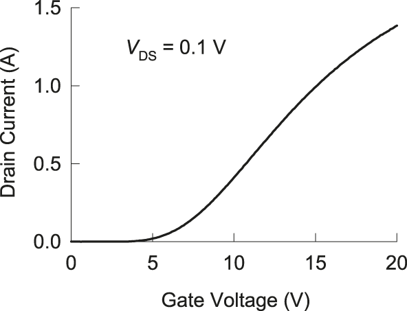
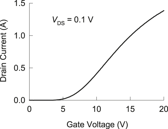
The transfer characteristics of a commercial MOSFET are shown in Figure 3. It can be seen that the turning ON of this MOSFET is gradual, and relatively high voltages of up to 25 V are needed to achieve a sufficient current. This problem still relates to issues of interface passivation, because a large fraction of the channel electrons are still trapped at and near the SiC–SiO2 interface. These MOSFETs provide a smaller ON resistance for a higher blocking voltage than the theoretical limit of Si, and, accordingly, they enable switch-mode power circuits with improved efficiency and, in combination with SiC Schottky diodes, significantly reduced size. Nonetheless, further reduction in trap density is theoretically possible, which would enable the performance of SiC MOSFETs to approach the theoretical limit of SiC (as illustrated in Figure 2).
The transfer characteristics of a commercial SiC metal oxide semiconductor field-effect transistor for power applications, measured with 0.1 V as the drain-to-source voltage (V DS). The gate voltage must increase from approximately 5 V (the threshold voltage) to 20 V (the operating voltage) to achieve sufficiently high drain current (approximately 1.5 A). The “slow” turning ON of this device is due to trapping of electrons that are attracted to the SiC–SiO2 interface by the gate voltage (the trapped electrons do not contribute to the drain current). The need for a high-operating voltage at the gate can be removed by reducing the density of traps near the SiC–SiO2 interface, which can be achieved by improving the quality of this interface. Reprinted with permission from Reference 6. © 2014 IEEE.
The potential of GaN
GaN is another wide energy gap material with a very high breakdown field—about 20% higher than in the case of SiC—which also makes it attractive for the development of power switches.Reference Baliga21–Reference Saito, Takada, Kuraguchi, Tsuda, Omura, Ogura and Ohashi25 An important difference from SiC is that GaN is usually grown on other substrates, most frequently on sapphireReference Cao, Biser, Ee, Li, Tansu, Chan and Vinci26–Reference Wang, Liao and Li28 but also on SiC wafers. When grown on SiC wafers, the combined material is more expensive than just SiC, and it exhibits a much higher density of defects than SiC. Because of the higher defect density in comparison to SiC and a higher cost in comparison to GaN grown on other substrates, GaN grown on SiC is not used for power-electronic devices; its use is for fabrication of blue (and consequently white) light-emitting diodes that utilize the wide and direct energy gap of GaN. The very high density of defects, as high as 108 cm–2, does not cause fatal short circuits and recombination centers that would inhibit the light-emitting operation. Encouraged by the fact that these defects are not fatal, power transistors for microwave applications have been developed and commercialized with GaN grown on Si substrates. Although the defect density in this material is even higher than that for GaN grown on sapphire, the cost of this material is significantly reduced by the cheaper Si substrate.
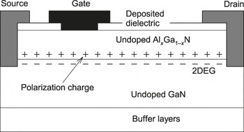
Commercial power transistors using GaN are based on a structure that is known as the high-electron-mobility transistor (HEMT), illustrated in Figure 4. As shown in the figure, the polarization charge due to the transition from GaN to AlxGa1–xN atomic bonds induces a two-dimensional electron gas (2DEG) at the GaN side of this heterojunction. Connecting the source and the drain, the 2DEG acts as the channel of this transistor. The name HEMT indicates that the mobility in the channel of the transistor is high, typically around 2000 cmReference Rabkowski, Peftitsis and Nee2/Vs, which is almost 100 times higher than in the case of electron mobility in the channel of SiC MOSFETs. This is a huge advantage in terms of the ability to achieve low ON resistance values by devices with a much smaller area. The high mobility of the electrons in the channel of HEMTs is enabled by the fact that the electron channel is formed at the heterojunction between undoped GaN and AlGaN, as illustrated in Figure 4. This heterojunction is created by in situ transition from GaN to AlGaN epitaxial growth and is atomically smooth without dangling bonds and defects that would trap electrons or reduce mobility by scattering. The energy gap of AlGaN is wider than the energy gap of GaN,Reference Pelá, Caetano, Marques, Ferreira, Furthmüller and Teles29,Reference Ren and Zolper30 which creates an energy barrier and prevents the electrons from the channel leaking into the gate of the device. The transition from GaN to AlGaN creates fixed and positive polarization charge, which attracts the electrons that create the channel.Reference Ambacher, Smart, Shealy, Weimann, Chu, Murphy, Schaff, Eastman, Dimitrov, Wittmer, Stutzmann, Rieger and Hilsenbeck31,Reference Wang, Wu and Wu32 The 2DEG channel indicates that the motion of electrons is restricted to two dimensions due to the quantum confinement of the electrons in the energy potential well at the heterojunction.
The cross-section of a high-electron-mobility transistor. The two-dimensional electron gas (2DEG), formed at the AlxGa1–xN–GaN heterojunction, acts as a channel that connects the source and the drain of electrons when the transistor is in ON mode. Negative voltage can be applied to the gate to remove the channel electrons under the gate, setting the transistor in OFF mode. Reprinted with permission from Reference 6. © 2014 IEEE.

The main advantage of the HEMT structure shown in Figure 4 is the inherently small output capacitance. The output of the device is the drain contact to the 2DEG, which is depleted under the gate when positive drain voltage is applied and the device is in OFF mode. Without overlap between the 2DEG and the gate electrode, there is no drain-to-gate capacitance other than the very small stray capacitance due to the lateral electric field between the 2DEG and the gate. The 2DEG connected to the drain is basically positioned over the undoped GaN layer, or very low doped but depleted GaN layer, which can be considered a dielectric. As a result, there is no drain capacitance, which is very different from the MOSFET structure where the drain capacitance is due to the capacitance of the drain-to-body p–n junction.
This difference in device structure results in a big HEMT advantage in terms of the possibility to almost eliminate the dynamic power dissipation, even in the case of high-voltage applications. To illustrate this advantage, consider that the output capacitance has to be charged to V B = 1000 V and then discharged again with a switching frequency of f = 100 kHz. For C out = 500 pF, which is a typical number for a SiC MOSFET, the dynamic power dissipation is P dynamic= fC outV BReference Rabkowski, Peftitsis and Nee2 = 50 W. For 1 kW power supply, this is a 5% loss due to the output capacitance alone. With a HEMT as the controlled switch, the dynamic-power loss due to the output capacitance becomes insignificant (much smaller than the static power loss).
The potential for cost reduction emerges as another big advantage of GaN-based technology. The cost reduction is not only due to the possibility to reduce the area of the device because of the high channel mobility, but also due to the inherently simpler fabrication of HEMTs in comparison to the SiC MOSFETs. There is no need for semiconductor doping or the growth of a gate oxide, and the number of needed photolithography steps is smaller. In addition to simpler and cheaper processing, GaN is grown on cheaper wafers with larger diameters in comparison to SiC wafers. The cost of the substrate could significantly be reduced if the efforts to grow device-quality GaN layers on larger than 150 mm Si wafers, or larger than 150 mm Si wafers covered by monocrystalline SiC,Reference Wang, Dimitrijev, Han, Iacopi, Hold, Tanner and Harrison33 are successful.
One disadvantage of the HEMT structure is that the current flow is lateral, and the power devices require both the source and drain contacts to be created at the surface. This results in less efficient utilization of the surface area in comparison to the vertical MOSFETs using SiC; however, that loss is smaller in comparison to the area gain that can be achieved by the 100 times larger electron mobility.
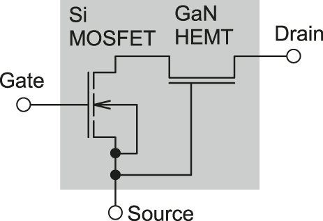
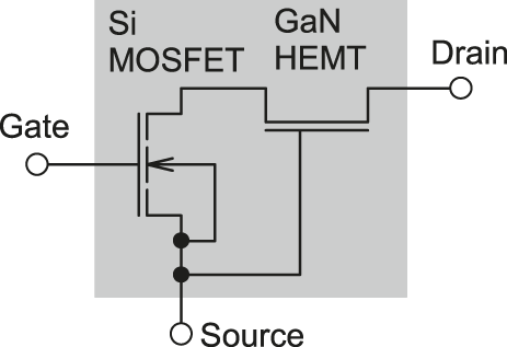
The most important disadvantage of the HEMT structure is that the 2DEG is created by the polarization charge, which means that the HEMTs are ON for zero gate voltage—a normally ON device. To turn the switch OFF, a negative gate voltage is applied. This feature is not a problem, and it appears to be an advantage when HEMTs are used as amplifiers for microwave applications. However, this is a very undesirable feature for HEMTs that would be used as power switches (the fourth key requirement for a power switch is the normally OFF operation). To resolve this problem, commercial GaN HEMTs are connected with a Si MOSFETReference Huang, Liu, Li and Lee34,Reference Huang, Li, Liu and Lee35 in the configuration shown in Figure 5, which is typically referred to as a cascode connection. As can be seen, the Si MOSFET provides the normally OFF operation, whereas the GaN HEMTs provide high-blocking voltage and low ON resistance. The ON resistance of the Si MOSFET is added to the ON resistance of the HEMT; however, the Si MOSFET is a low-voltage device with a small ON resistance because it does not require a drift region.
Cascode connection between a Si metal oxide semiconductor field-effect transistor (MOSFET), which provides normally OFF operation, and a GaN high-electron-mobility transistor (HEMT), which provides a high-blocking voltage.
The cascode connection between a Si MOSFET and GaN HEMT enables the advantages of GaN HEMTs to be practically utilized; however, it is not the ideal solution. With this potential to significantly reduce the cost of power switches created in GaN, it becomes very attractive to work on the problem of normally OFF conduction and to create a normally OFF HEMT. Many research activities are guided by this insight.Reference Cai, Zhou, Lau and Chen36–Reference Zhou, Chen, Piner and Chen42 Some of the approaches have included the use of a gate material with a larger work function, while others have focused on introducing negative charge in the gate area, and yet another approach is to deposit a p-type doped GaN or AlGaN layer on top of the AlGaN barrier. A gate dielectric between the gate metal and the AlGaN film is used to reduce the gate leakage. The structure created by utilizing a gate dielectric is usually referred to as a MOS-HEMT. If this effort is successful and a normally OFF HEMT or MOS-HEMTReference Dong, Tan, Cai, Chen, Liu, Xu, Xue, Yu, Wang, Zhao, Hou, Chen and Zhang43–Reference Liu, Chou, Hsu, Lee, Sheu and Ho47 is developed, it has the potential to become the dominant device because of the significant power dissipation and cost advantages.
Summary
Si MOSFETs and Si diodes have enabled the development of switch-mode circuits for efficient power conversion (AC to DC, DC to AC, DC to DC), especially for power management in information technology and consumer electronics. Progress by further development of Si-based devices has saturated due to the material limits discussed in this article, leaving much potential for the development of high-voltage devices (above 1000 V) for switching applications (automotive applications, inverters for industrial applications, uninterruptable power supplies, inverters for DC transmission of electric energy). This development necessitates the use of materials with much higher breakdown fields (wider energy gaps), the two main contenders being SiC and GaN. Both SiC Schottky diodes (the preferred diode structure because of its switching speed) and SiC MOSFETs have already been commercialized. At present, SiC is evolving as the power-device material for applications that require blocking voltages higher than 1000 V. Further progress can be made toward the theoretical limit of SiC, enabling new applications by switches with increased blocking capabilities and enabling higher power-conversion efficiencies by switches with reduced ON resistances. It is also likely that further development and adoption of SiC devices will result in continued cost reduction of SiC-based power electronics. Furthermore, the potential of HEMT as a controlled switch in GaN is high. The two main advantages are improved power efficiency due to inherently small output capacitance and the potential for significant cost reduction (cheaper substrates and simpler processing). If these advantages are realized, GaN HEMTs will complement the high-voltage applications based on SiC MOSFETs.