


I. INTRODUCTION
Modern wireless technology should provide high reliability and channel capacity requirements of wireless communication systems. These goals can be achieved by utilizing the multiple-input–multiple-output (MIMO) technology [Reference Paulraj, Gore, Nabar and Bölcskei1]. MIMO technology introduces several advantages such as high datarates and high capacity [Reference Zhang, Wang, Yu and Huang2, Reference Fakhr3]. Antennas of a MIMO communication system consist of multiple elements, hence high isolation has to be achieved between these antenna elements for efficient operation of different space–time transmission techniques [Reference Li, Xiong and He4]. Several attempts have been made to reduce the mutual coupling effect between the antenna elements in MIMO systems. These attempts include the use of electromagnetic bandgap (EBG) structures to reduce the surface wave [Reference Zhang, Castaneda and Alexopoulos5–Reference Yang, Fan, Chen, She and Feng9]. However, these structures are complex to design as well as occupy a comparatively large area. On the other hand, defected ground structures (DGSs) are implemented by etching slots of different shapes in the ground plane. Different shapes of DGS have been proposed for increasing the isolation between the two antennas [Reference Abdel-Rahman, Verma, Boutejdar and Omar10–Reference Hajilou, Hassani and Rahmati16]. A DGS resonator is equivalent to a resonance LC network, which can be used to generate a stopband. This stopband can decrease the propagation of the surface waves and hence can decrease the mutual coupling between the MIMO antennas. The slot antenna can give a resonance and force the power that tends to couple from one antenna to the other to radiate into free space directly. When the resonant frequency of the slot is near the microstrip antenna's operating frequency, the isolation is also high.
In this paper, we propose a slot structure in the ground plane between two antenna elements to suppress the surface wave between the elements. The theoretical modeling of the DGS filter has been introduced and verified by electromagnetic full wave simulations. The commercial software CST microwave studio has been employed. The design and performance of the DGS bandstop filter application to the two elements MIMO antennas has been introduced through full wave simulation and practical measurement. The DGS slot dimensions and positions are optimized to obtain maximum coupling reduction with minimum dimensions. The theoretical concepts of the designed MIMO antenna are introduced. Analysis of mutual coupling, correlation coefficient, diversity gain, and total active reflection coefficient (TARC) is presented. Finally, the simulated results are confirmed by the experimental measurements.
II. DGS RESONATOR
A DGS resonator in the ground plane structure excited by 50 Ω microstrip transmission line is shown in Fig. 1(a). The structure is designed on substrate FR4 with relative permittivity = 4.4, a dielectric loss tangent = 0.025, and thickness (h) = 1.6 mm. The equivalent circuit model for this structure is the LC tank circuit shown in Fig. 1(b). The DGS resonator was designed by using a slot of width = 1.4 mm and length = 20 mm. in the ground plane. The values for L p and C p are obtained in terms of the 3 dB cut-off frequency (f c) in GHz and pole frequency (f p) in GHz as [Reference Abdel-Rahman, El Dein, Hamed and Ibrahim17]
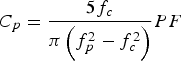 $$C_p = \displaystyle{5f_c \over \pi \left(f_p^2 - f_c ^2 \right)} PF$$
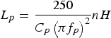 $$L_p = \displaystyle{250 \over C_p \left(\pi f_p \right)^2} nH$$
From (1), it is clear that, C p = 0.5 pF and L p = 1.53 nH. The performance of the DGS bandstop filter has been validated by simulating its scattering parameter magnitudes by using full wave simulations and its circuit simulation. A comparison between the simulated results is shown in Fig. 2. It is noticed that there is good agreement between the two simulations which confirms the DGS bandstop design. From Fig. 2, it is obvious that there is an attenuation resonance at 5.8 GHz. Also, we can extract f c = 4.4 GHz, and f p = 5.8 GHz at which the S 21 magnitude is lower than −30 dB.
(a) 3D view of the DGS microstrip resonator. (b) The equivalent circuit of the resonator.

EM and equivalent circuit simulated results for the scattering parameters magnitudes of a microstrip loaded with a DGS unit.
III. MICROSTRIP MIMO ANTENNA
The two antennas are put all together on the same FR4 substrate whereas the space between the two antennas was optimized to 0.058λ 0 as shown in Fig. 3(a). Also, the fabricated antenna is shown in Fig. 3(b). The measured and simulated scattering parameter magnitudes of the two elements microstrip MIMO antenna are shown in Fig. 4. From the shown simulated results, it is obvious that the antenna is operating at 5.8 GHz at which the return loss lower than 15 dB with bandwidth equals 190 MHz from 5.72 to 5.91 GHz, approximately. On the other hand, the isolation between the two ports is only 15 dB at the operating frequency. From the measured results it is clear that, the fabricated microstrip MIMO antenna operates at 5.87 GHz, approximately, with almost 15 dB return loss and almost 15 dB mutual coupling. A good agreement is achieved between the simulated and the measured results. However, there is a small frequency shift between the two results. This can be as a result of the imperfection between the full wave and the fabrication process which cannot be totally avoided.
(a) 2D layout of the microstrip MIMO antenna. (b) A photograph of the fabricated MIMO antenna.
Scattering parameter magnitudes of the simulated and the measured results of the microstrip MIMO antenna.
The visualization of the surface wave propagating inside the dielectric substrate is illustrated in Fig. 5. It is clear that the field of the first element can cross the second antenna element which increases the mutual coupling between them. Also, from Fig. 5 it can be concluded that that the surface current in between the two antenna elements is high hence, the DGS filter which is illustrated in the previous section is designed to introduce a stop band at 5.8 GHz which is the desired antenna operating frequency. Therefore, mutual coupling between the two antenna elements is expected to be reduced.
Total electric field inside the substrate for z = 1 mm from the ground plane.
IV. PROPOSED MIMO ANTENNA
The fabricated proposed MIMO antenna is demonstrated in Fig. 6. A DGS slot has been etched in the ground between the two patches for the purpose of reducing the mutual coupling between the two antennas as shown in Fig. 6(b). The DGS slot dimensions and positions are optimized to obtain maximum coupling reduction with minimum dimensions. The measured and simulated scattering parameter magnitudes of the proposed MIMO antenna are shown in Fig. 7. From the simulated results, it is clear that the operating frequency of the antenna is slightly shifted from 5.8 to 5.86 GHz. This shift was due to the presence of the DGS structure which affect the fringing field between the two patches which can affect the whole antenna element electrical length and hence resonance frequency. The return loss is higher than 15 dB with bandwidth equaling 190 MHz from 5.77 to 5.96 GHz approximately. On the other hand, the mutual coupling, expressed in terms of transmission coefficient S21, is reduced from −15 to −28 dB when the DGS structure is used at the operating frequency. The reduction in mutual coupling is due to the slot antenna that can resonate the power that tends to couple from one antenna to the other to radiate into free space directly. This requires that the resonant frequency of the slot is near the microstrip antenna's operating frequency. From the measured results, it is clear that the fabricated proposed MIMO antenna operates at 5.9 GHz, approximately, with almost 15 dB return loss and 28 dB mutual coupling. Good agreement is achieved between the simulated and the measured results.
A photograph of the fabricated proposed MIMO antenna (a) top view and (b) bottom view.
Scattering parameter magnitudes of the simulated and the measured results of the proposed MIMO antenna.
To study the effect of the length of the DGS slot (L) on the performance of the MIMO antenna, a parametric study has been conducted. The S-parameter magnitudes (S 11 and S 21) of the MIMO antenna at different lengths of the DGS slot are shown in Fig. 8. The width of the DGS slot is 1.4 mm. It is noticed that the isolation of this structure is sensitive to the length of the DGS slot (L). The maximum isolation is achieved when the length of the slot equals 20 mm. This means that the effect of the isolation is obtained at the resonance frequency of the slot as discussed before in section II.
Scattering parameter magnitudes of the simulated MIMO antenna with varying L (a) S 11 optimization and (b) S 21 optimization.
The simulated directive gain patterns of the proposed two elements MIMO antenna in E and H planes at 5.8 GHz are shown in Fig. 9 for radiation at ports 1 and 2, respectively. This can be obtained when port 1 is fed and port 2 is terminated by matching load and vice versa. From Fig. 9, the proposed MIMO antenna presents back radiation which is due to the effect of the rectangular slot. This means that the slot introduces radiation at resonance frequency, which is helpful for increasing the isolation between the two ports.
The Simulated directive gain of two elements MIMO antenna at 5.8 GHz (a) E and (b) H plane at port 1 (c) E and (b) H plane at port 2.
The simulated efficiency and the peak gain through the entire bandwidth of the MIMO antenna with and without slot are illustrated in Figs. 10(a) and 10(b), respectively.
(a) The antenna total efficiency. (b) The antenna gain.
We can observe that the antenna efficiency, in Fig. 10(a), at the center frequency without using DGS (5.8 GHz) is 53% and it is reduced to 48% on using the DGS, at the same frequency. On the other hand, at the center frequency on using the DGS (5.86 GHz), it is 54%, whereas it is 57% without using the DGS, at the same frequency. Therefore, we can claim that the average value of the efficiency without using the DGS (55%) is dropped to 51% on using the DGS. This demonstrates the little effect of the DGS on the antenna efficiency.
On the other hand, in Fig. 10(b), the gain at the center frequency without using DGS (5.8 GHz) is 3.3 dB and it is increased to 3.4 dB on using the DGS, at the same frequency. On the other hand, at the center frequency on using the DGS (5.86 GHz), it is 3.65 dB, whereas it is 3.45 dB without using the DGS, at the same frequency. Therefore, we can claim that the average value of the efficiency without using the DGS is 3.37 dB, which is increased to 3.52 dB on using the DGS.
Finally, the visualization of the surface wave propagating inside the dielectric substrate with slot is illustrated in Fig. 11. It is clear that the slot prevents most of the field from crossing the second element, which means that the mutual coupling between the antenna elements is decreased.
Total electric field inside the substrate for z = 1 mm from the ground plane with slot.
Several parameters such as envelope correlation coefficient, diversity gain, and TARC have been calculated to measure the performance of the MIMO antenna. The first parameter is the envelope correlation, which measures the correlation between the antenna elements in the MIMO system. Therefore, for the best performance of the MIMO system, the correlation between the two antenna elements has to be as low as possible. The envelope correlation coefficient between the two antenna elements in terms of the S-parameters is given by [Reference Blanch, Romeu and Corbella18]. The envelope correlation coefficient has been calculated under the assumption of uniform multipath environment as (2)
 $$\rho_e = \displaystyle{\left\vert S_{11}^{\ast} S_{12} + S_{21}^{\ast} S_{22} \right\vert^2 \over \left(1 - \lpar \left\vert S_{11} \right\vert^2 + \left\vert S_{21} \right\vert^2\rpar \right)\left(1 - \lpar \left\vert S_{22} \right\vert^2 + \left\vert S_{12} \right\vert^2\rpar \right)}$$
A comparison between the envelope correlation coefficient of the MIMO antennas with and without slot is shown in Fig. 12. It is obvious that the envelope correlation coefficient of the MIMO antenna thorough the entire bandwidth without slot equals 0.17 at 5.72 GHz and is reduced to 0.008 at 5.8 GHz and increased from 0.04 to 0.06 at the end of the upper frequency bands. On the other hand, the envelope correlation coefficient of the proposed MIMO antenna equals 0.02 at 5.77 GHz and is reduced to 0.003 from 5.86 to 5.95 GHz. The relationship between the envelope correlation and the diversity gain has been calculated as [Reference Rosengren and Kildal19]
 $$Gapp = 10\sqrt{1 - \left\vert \rho \right\vert}\comma \; \quad {\rm where }\, \rho_e = \left\vert \rho \right\vert$$
The diversity gain of the MIMO antenna with and without slot is illustrated in Fig. 13. It is clear that the diversity gain of the MIMO antenna with slot is better than without slot. The diversity gain of the MIMO antenna with slot equals around 9.99 dB within the frequency band however, the MIMO antenna without slot introduces diversity gain equals 9.86 dB at the beginning of the frequency band at 5.72 GHz and increased around 9.99 dB at 5.8 GHz and then decreased to 9.98 dB at the end of the frequency band. The efficiency of the MIMO antenna is also measured by a parameter called TARC. TARC is defined as the ratio of the square root of total reflected power divided by the square root of total incident power [Reference Manteghi and Rahmat-Samii20]. TARC can be defined as the return loss of the whole MIMO antenna elements [Reference Manteghi and Rahmat-Samii20]. The TARC has been calculated from the scattering parameters of two antenna elements as [Reference Chae, Oh and Park21].
 $$TARC = \sqrt{\displaystyle{\left\vert S_{11} + S_{12} e^{j\theta} \right\vert^2 + \left\vert S_{21} + S_{22} e^{j\theta} \right\vert^2 \over 2}}$$
where θ is considered a variable angle which is related to the phase of the excitation signal. Random phased excitation vectors have been used to calculate average TARC and the MIMO channel is assumed to be Gaussian and multipath spread in the propagation channel [Reference Manteghi and Rahmat-Samii20]. TARC is calculated at each random phase between 0 and 180. A comparison between the MIMO antennas with and without slot is demonstrated in Fig. 14. It is noticed that the TARC with slot equals −24 dB but the TARC without slot equals −18 dB at 5.8 GHz. From the previous investigations it is claimed that the performance of the MIMO antenna is improved when a simple rectangular slot is loaded between the antenna elements.
Envelope correlation coefficient of the MIMO antenna with and without slot.
Diversity gain of the MIMO antenna with and without slot.
TARC of the MIMO antenna with and without slot.
The previous results of the MIMO antenna are compared with different approaches such as DGS, EBG, and metamaterial structures. A fair compassion requires the use of the same antenna element type with the same antenna element separations which is quite difficult. However, we introduce some examples with similar specification to our proposed MIMO antenna. First, some achievements for the coupling reduction between the two antenna elements by using DGS structures are presented in [Reference Hajilou, Hassani and Rahmati16, Reference Vazquez, Hotopan, Ver Hoeye, Fernandez, Herran and Las-Heras22]. In [Reference Hajilou, Hassani and Rahmati16], the mutual coupling is reduced to 35 dB but the two antenna elements are separated by 0.25λ 0, which increases the total size of the antenna in addition to the complexity of the DGS structure which is used in that paper. Also, in [Reference Vazquez, Hotopan, Ver Hoeye, Fernandez, Herran and Las-Heras22], the mutual coupling is reduced to 28 dB when three rectangular slots are used and the space between the antenna elements equals 0.7λ 0. We can observe that we achieve similar results for very smaller separation (0.058λ0). Second, in [Reference Tariqul Islam and Shahidul Alam23], the mutual coupling between the antenna elements is reduced by using the EBG structure. The mutual coupling is reduced to 35 dB when 3 × 3 EBG cells are used between the two antenna elements and the separation between the antenna elements equals 0.47λ 0. We can notice that not only the over size of the antenna is increased but also the complexity of the EBG structure is introduced compared to our proposed MIMO antenna whereas the mutual coupling is almost similar. Finally, the metamaterial structure is used to reduce the mutual coupling between the antenna elements in [Reference Bait-Suwailam, Siddiqui and Ramahi24]. The mutual coupling is reduced to 27 dB when three cells of slotted complementary split ring resonator (CSRR) are used. However, the space between the antenna elements equals 0.25λ 0, which is not considered a small one. From the previous comparison, we can claim that our MIMO antenna can introduce a very challenging antenna with simple and compact overall size compared to others.
V. CONCLUSION
In this paper, a close and high isolation microstrip two element patch MIMO antenna is introduced. The two-antenna elements are operating at 5.8 GHz for wireless applications. The reduction of the mutual coupling between the antenna elements has been achieved by using DGS. The separation between the edges of the two elements has been achieved to be only 0.058λ 0. The analysis of the correlation coefficient, diversity gain and TARC are presented to evaluate the performance of the MIMO antenna. Experimental measurements are introduced to verify the MIMO antenna with high isolation design in full-wave simulations. The results confirm that the isolation between the elements of the proposed MIMO antenna is 28 dB at 5.8 GHz and the envelope correlation equals 0.003. A good agreement has been achieved between the simulated and the measured results.
 Ahmed A. Ibrahim was born in 1986. He received the B.Sc. degree, with grade of very good, in electrical engineering from the Electronic and communication Engineering Department, Elminia University, Elminia, Egypt in 2007. He was awarded the M.Sc. degree in electronic and communication engineering from Elminia University in 2011. He is currently working toward the Ph.D. degree in communication and microwave engineering at the faculty of engineering, Elminia University, Egypt. His research interests include the design and analysis of microstrip antennas, microstrip filters, and its application in wireless communications. Also, metamaterial MIMO antenna and different metamaterial applications in microwave bands.
 Mahmoud A. Abdalla was born in 1973. He received the B.Sc. degree, with grade of excellent with honors, in electrical engineering from the Electronic Engineering Department, Military Technical College, Cairo, Egypt in 1995. He was awarded the M.Sc. degree in electrical engineering from Military Technical College in 2000, and the Ph.D. degree from microwave and communication group, School of Electrical Engineering, Manchester University, UK, in 2009. He has been with Military Technical College since 1996 where he is now a lecturer in the Electronic Engineering department. His research has focused on different metamaterial applications in microwave and millimeter bands specially microwave components, miniaturized multiband antennas, and ferrite components. Also, his research includes electromagnetic energy harvesting systems, EBG components, adaptive antenna systems for DOA estimation and interference cancellations, and radar absorber designs. He has published more than 60 peer-reviewed journal and conference papers. Dr Mahmoud Abdalla is currently a reviewer in many electromagnetic journals such as IEEE Antennas and Wireless Propagation Letters, IEEE transaction in Magnetics, Progress in Electromagnetic Research, European Physical Journal – Applied Physics, Journal of electromagnetic waves (JEMW), Advanced Electromagnetic, and International Journal of Microwave and Wireless Technologies. He is also a member of the IEEE and the European Microwave Association (EuMA).



