I. INTRODUCTION
Packaging has a critical impact on high-efficiency high-power RF transistors as it greatly determines and limits the fundamental and harmonic loads of the internal transistor die. Therefore, scalability and reliability of the package modeling are essential issues that must be addressed during the design cycle of packaged GaN HEMTs.
Different modeling techniques of RF packages have already been published. Full-wave electromagnetic (EM) simulations are often used [Reference Johansson and Arnborg1, Reference Flucke, Schmückle, Heinrich and Rudolph2], but they are very time consuming and not easily scalable. Other approaches consist of extracting an equivalent circuit model of the package from EM simulations [Reference Liang, Plá, Aaen and Mahalingam3] or S-parameter measurements of coplanar standards placed inside the package [Reference Chun, Pham, Laskar and Hutchison4]. More recently, in the case of an RF package integrating a silicon LDMOS power transistor and its matching MOS capacitors, Aaen et al. [Reference Aaen, Plá and Balanis5, Reference Aaen, Plá and Balanis6] proposed a modeling technique based on a combination of EM simulations with equivalent circuit extractions for the segmentation of the complex packaging environment into its constituent components. A complete insight into the topics of nonlinear transistor modeling, parameter extraction techniques, and package effects can be found in [Reference Aaen, Plá and Wood7, Reference Rudolph, Fager and Root8]. In this paper, we propose a modeling method of packaged GaN HEMTs in S-band associating a nonlinear model of the GaN HEMT die with a lumped-element circuit model of the package. Despite the simplifying assumptions of lumped-element models compared with all possible EM interactions at high frequencies, the modeling time can be dramatically reduced thereby allowing the designers to optimize the package configuration since each of its physical constituents is linked to a lumped-element circuit. Our aim is to enable a rapid Computer aided design (CAD) synthesis of the optimum package for internally matched GaN HEMTs in S-band that can be compatible with the required nonlinear simulations to optimize power and efficiency performances.
Section II describes the modeling method and illustrates its scalability through the modeling of two different package configurations for the same 20 W GaN HEMT in S-band. Although both package models of Section II are validated by using conventional S-parameter measurements, Section III illustrates the most important validation step for power applications in the case of the second package configuration by using both frequency- and time-domain power measurements.
II. EXTRACTION METHODOLOGY OF THE PACKAGE MODEL
A) On-wafer pulsed measurements of the GaN HEMT die
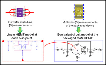
The modeling process starts with on-wafer pulsed-IV and pulsed-RF measurements of the GaN HEMT die which are performed at different bias points (Fig. 1) to extract the nonlinear model of the transistor [Reference Jardel9]. Such a nonlinear model is crucial for the validation step under large-signal operating conditions that will be presented in the last section. In addition, a linear model (LM) of the transistor chip is extracted at each bias point to be used during the modeling/synthesis procedures of its dedicated package. During this classical procedure for extracting the linear HEMT model, the cut-off bias is one of the multi-bias conditions, which is used at low frequencies for assessing the values of intrinsic capacitances Cgs, Cds, and Cgd of the transistor die. It should be noted that the proposed modeling method assumes that the designer can measure both the transistor die and the packaged transistor, which is not always the case.
On-wafer measurements and LM of the GaN die.

B) S-parameter measurements of the packaged device
S-parameter measurements of packaged devices require the design of specific test fixtures. Consequently, a dedicated 50 Ω test fixture was designed to measure the packaged GaN HEMT (Fig. 2(a)). A 1.6-mm-thick duroïd substrate with a low dielectric constant (ɛ r = 2.2) was selected so as to minimize the width discontinuity between 50 Ω lines (4.8 mm wide) and the package leads (5.5 mm wide). Afterwards, multi-bias S-parameter measurements were performed on the packaged transistor mounted in the test fixture, using the same bias points as those previously used for the nonlinear modeling of the transistor die. In order to remove the effects of the test fixture for determining the de-embedded measurements of the packaged device [Reference Rytting10], a Thru-Reflect-Line (TRL) calibration kit (Fig. 2(b)) was designed and optimized on duroïd substrate for applications up to 7 GHz.
(a) 50 Ω test fixture; (b) TRL calibration kit.

C) Architecture of the lumped-element package model
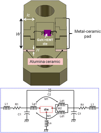
In S-band, the primary elements of metal-ceramic packages influencing the power performances of the GaN HEMT die are the package capacitances, the self and mutual inductances of bond wires, the coupling between input and output ports of the package, and the internal matching circuits. As pointed out in the introduction, the requirement of carrying out time-domain simulations for optimizing high-efficiency performances of packaged power transistors led us to adopt a lumped-element modeling approach. The passive components and interconnects of the package are modeled by equivalent electrical models, which are connected to the LM of the internal GaN HEMT die. Fig. 3 shows an example of equivalent circuit model for an initial package configuration integrating the gate, drain, and source bond wires of the device. In this package example (Fig. 3), the gate bond wire, the two parallel drain bond wires, and the four source bond wires are modeled by the equivalent inductances Lg 1, Ld 1, and Ls, respectively. The mutual inductances M 1 and M 2 are used to model the coupling between gate and drain wires, and the coupling between both drain wires, respectively. The four source bond wires are far away so as to be only modeled by their equivalent inductance Ls.
Example of architecture of the lumped-element package model.

The metal-ceramic input/output pads located on both sides of the package are modeled by a shunt–series–series C 1–R 1–L 1 circuit as shown in Fig. 3. The input/output capacitance C 1 is determined by the substrate thickness H and the surface area of the metal-ceramic pad. The resistance R 1 corresponds to the metallic losses of the leads while the inductance L 1 represents parasitic effects between the package leads and the 50 Ω lines of the test fixture. The capacitance C 2 represents the forward-coupling effect of the metal-ceramic package.
In S-band, the most critical elements are the package capacitance C 1 and the bond wires (Lg 1, Ld 1), while the other elements only have an impact on harmonic frequencies.
D) Extraction of the lumped-element package model
Before optimizing the values of each lumped element that make up the package model in order to achieve the best fit between measured and simulated multi-bias S-parameters, we need to define initial values for the lumped elements.
Assessing the values of the self and mutual inductances of bond wires is the most difficult step of the model initialization. However, specific calculation methods have already been published to estimate the equivalent self and mutual inductances of bond wires given their size and the distances between them. In the following equations [Reference Grover11] of self and mutual inductances, l and r are the length and radius of the bond wire in μm, and d is the distance between wires in μm.
 $$L\left({{\rm nH}} \right)= 0.0002 \times l \times \left[{\ln \left({\displaystyle{{2 \times l} \over r}} \right)- 0.75} \right]$$
 $$M\left({{\rm nH}} \right)= 0.0002 \times l \times \left[{\ln \left({\displaystyle{l \over d} + \sqrt {1 + \displaystyle{{l^2} \over {d^2}}} } \right)- \sqrt {1 + \displaystyle{{d^2} \over {l^2}}} + \displaystyle{d \over l}} \right]$$
In order to take into account the wire shape and its height from the ground plane, the initial values of self and mutual inductances are adjusted using the Philips model [Reference Mouthaan, Tinti, De Kok, De Graaff, Tauritz and Slotboom12] available in Agilent's Advanced Design System.
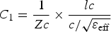
The value of C 1, which represents the package capacitance, is calculated using the following equation:
 $$C_1 = \displaystyle{1 \over {Zc}} \times \displaystyle{{lc} \over {c/\sqrt {\varepsilon _{{\rm eff}} } }}$$
where c is the speed of light, ɛ eff is the effective dielectric constant of the alumina substrate, while lc and Zc are the length and characteristic impedance of the metal-ceramic pad, respectively.
The values of Zc and ɛ eff are calculated from the dielectric constant ɛ r of the substrate and the aspect ratio (width/height) of the metal-ceramic pad using the equations reported in [Reference Bahl and Trivedi13]. In the case of our package (Fig. 3), the characteristics of the metal-ceramic pads are (lc = 1.5 mm, ɛ r = 9.9, W/H = 12.5) giving the following initial values (Zc = 8 Ω, ɛ eff = 8.7, C 1 = 2 pF). Furthermore, given the cavity dimensions, EM simulations of the empty package were performed for determining the coupling capacitance C 2 between package ports, and checking that the internal cavity is free of any resonance in the frequency range of interest.
Then, using the set of bias-dependent LMs of the GaN HEMT die which were previously extracted from on-wafer measurements, the initial model of the packaged device at a given bias point is constructed by connecting the LM of the GaN HEMT die at this particular bias point to the lumped elements of the package model (Fig. 3). Therefore, we obtain a set of bias-dependent models of the packaged device which share the same values of passive-lumped elements for the package model which must be bias-independent. It can be noted that the cut-off bias, which is one of the multi-bias conditions of the measurement process, allows to assess the capacitance values of the package at low frequencies given that the intrinsic capacitances of the transistor die are already determined within the model of the transistor die.
Finally, by implementing all these bias-dependent models of the packaged GaN HEMT in the same simulation template, their identical lumped elements related to the package model are optimized to best fit the set of multi-bias S-parameter measurements performed on the packaged device (Fig. 4). Starting from the initial values of passive lumped elements for the package model, their optimized values are forced to remain within a limited range of variation so as to ensure that their final values remain closely linked to the nature and dimensions of the package constituents.
Extraction procedure of package model (e.g. first package configuration).

Such a constraint is very important as the physical constituents of the package (bond wires, metal-ceramic pads, etc.) have to be closely linked to their equivalent lumped elements in order to allow an efficient die-package co-design for power matching. Fig. 4 illustrates the extraction method of the package model in the case of the first package configuration.
III. PACKAGE MODELING RESULTS AND MEASUREMENTS
This modeling method was applied to a 20 W AlGaN/GaN HEMT die with 2.4 mm gate width from the GH50_10 GaN process available at UMS. A metal-ceramic power package suitable for use in S-band was selected with dimensions of 5.84 × 6.6 mm2 so as to allow the integration of internal matching circuits.
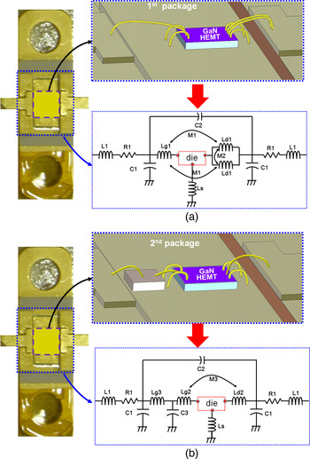
Two different package configurations were realized in order to optimize power performances and highlight the scalability of this modeling method. Both package configurations are represented in Fig. 5.
(a) First and (b) second packages of the GaN HEMT and their lumped-element equivalent circuits.

In both cases, the input and output metal-ceramic pads were made of a metallic plate of Alloy-42 (6.3 mm wide, 1.5 mm long) on a 0.5-mm-thick alumina substrate. The surface area of the metal plate and the substrate thickness determine the value of the capacitance C 1. It should be noted that the output capacitance C 1 is of prime importance for the harmonic matching of the power GaN HEMT [Reference Chéron14] because it allows the second-harmonic loads seen by the internal die to be confined to high-efficiency regions whatever the impedances presented outside the package. Therefore, in the case of this GaN HEMT die, the required value of C 1 (~2 pF) was synthesized by realizing the suitable width (W = 6.3 mm) of the output metal-ceramic pad (lc = 1.5 mm, H = 0.5 mm).
In the case of the first package configuration (Fig. 5(a)), a single 1.8 mm long bond wire Lg 1 connects the input metal-ceramic pad to the gate pad, a pair of 1.3 mm long bond wires Ld 1 connects the drain pad to the output metal-ceramic pad, and four 0.6 mm long bond wires Ls connect the source pads to the flange. All connections use 38 µm diameter gold wires. Fig. 5(a) shows the equivalent circuit schematic of the first package configuration wherein the red box denotes the bias-dependent model of the GaN HEMT die.
Once a set of lumped-element values has been determined for the first package using the modeling method presented in the previous section, it becomes easier to design an internally matched packaged GaN HEMT by optimizing the package constituents (i.e. its lumped elements) to get the desired power characteristics in time and frequency domains. Hence, starting from the first package, an internally matched package was synthesized and fabricated to achieve improved power performances of the GaN HEMT die in S-band.
The second package structure and its equivalent circuit are shown in Fig. 5(b). The cavity dimensions, the GaN HEMT die, and the source bond wires are unchanged, while the second package integrates internal pre-matching circuits with optimized lengths of the gate and drain bond wires. The input pre-matching circuit consists of a shunt MOS capacitor (C 3 = 8.2 pF), which is connected to both the gate and the input pad by using optimized wire lengths of 0.7 mm and 1.2 mm for the inductances Lg 2 and Lg 3, respectively. The output pre-matching circuit integrates the required low-pass filter (Ld 2-C 1) for harmonic matching [Reference Chéron14], wherein the optimum inductance Ld 2 is realized by a 2.2 mm long bond wire between the drain pad and the output metal-ceramic pad. The three bond wires Lg 2, Lg 3, and Ld 2 have a 17 µm diameter.
A) Small-signal validation of packaged GaN HEMTs
This section shows the comparison of measured and simulated S-parameters for both package configurations. Tables 1–3 list the values of equivalent circuit elements.
Lumped elements of metal-ceramic pads and source bond wires.

Lumped elements of the first package.

Lumped elements of the second package.

Figs 6 and 7 compare S-parameter measurements with electrical model simulations for the first and second package configurations, respectively.
Measured and simulated S-parameters of the packaged GaN HEMT (first package configuration) at (Vds0 = 50 V, Ids0 = 40 mA) from 1 to 7 GHz.

Measured and simulated S-parameters of the packaged GaN HEMT (second package configuration) at (Vds0 = 50 V, Ids0 = 40 mA) from 1 to 7 GHz.

In both figures, measurements and simulations are illustrated at the optimum bias point (Vds 0 = 50 V, Ids 0 = 40 mA) for maximum power added efficiency (PAE). In both cases, the equivalent circuit model achieved good agreement with measurements up to 7 GHz. In the case of high-efficiency power operation, it should be noted that the package model must remain valid up to the highest second harmonic frequency since the second harmonic load impedances have a great impact on power-added-efficiency.
The nonlinear model of the 2.4 mm GaN HEMT die has been extracted using on-wafer pulsed-IV and pulsed-RF measurements [Reference Jardel9]. Finally, the nonlinear model of the packaged device associates the nonlinear model of the GaN HEMT die with the passive lumped elements of the second package configuration.
In order to check the reliability of this package model under large-signal operation for pulsed radar applications, pulsed load-pull measurements have been performed on the packaged GaN HEMT at the fundamental frequency of 3.2 GHz. The RF input power was pulsed using a 10 µs pulse width at a 10% duty cycle. Bias voltages were continuous with a gate bias voltage slightly above pinch-off and a drain bias voltage set to 50 V for maximizing PAE performances.
Figs 8 and 9 compare the power measurement results at 3.2 GHz with the nonlinear simulations of the packaged GaN HEMT under the same operating conditions. It should be noted that the choice of a lumped-element package model is of prime importance to enable such nonlinear simulations under pulsed conditions.
Measured and simulated load-pull contours of constant PAE and constant output power in the complex plane of the load reflection coefficient (Gamma_Load) at 3.2 GHz and 29 dBm input power.

Comparison between measured and simulated output power, PAE, gain and optimum loads when the packaged GaN HEMT is loaded on its optimum load impedance (ZL Opt−PAE) for maximum PAE at 3.2 GHz.

At 29 dBm input power, Fig. 8 shows a comparison between measured and simulated load-pull contours of constant PAE and constant output power in the ranges 50–70% and 40.5–42.5 dBm, respectively. A good agreement is achieved between simulations and measurements. These results are of prime importance for power amplifier design because they allow the designers to select the optimum load impedance providing the best trade-off between output power and PAE.
At 3.2 GHz, Fig. 9 shows the comparison between measured and simulated output power, PAE and gain versus input power when the packaged GaN HEMT is terminated by its optimum load impedance (ZL Opt–PAE) for maximum PAE. The packaged GaN HEMT exhibited 70% PAE associated with 42.5 dBm output power and 13.5 dB gain at 29 dBm input power.
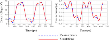
At the same time and under the same conditions, the output time-domain waveforms of the packaged GaN HEMT have been measured at 3.2 GHz with Agilent's PNA-X network analyzer. Using the lumped-element equivalent circuit of the package, the measurements at package plane were shifted to drain plane. Fig. 10 shows quite good agreement between measured and simulated time-domain waveforms of the drain voltage and current.
Comparison of measured and simulated time-domain waveforms at the drain plane of the GaN die at 3.2 GHz and 29 dBm input power.

Indeed, when compared with frequency measurements, these time-domain waveforms are more visual to assess the operating mode of the internal GaN HEMT die, when placed inside the package. They also allow the designer to assess the voltage/current swings within the limits of the safe operating area. Such an insight into the intrinsic large-signal behavior of the packaged GaN HEMT die is made possible through the use of a lumped equivalent circuit model of the package.
IV. CONCLUSION
This study highlights the advantages of a lumped-element package model for designing high-efficiency hybrid power amplifiers in S-band. At first, the nonlinear model of the transistor die is extracted from on-wafer pulsed-IV and pulsed-RF measurements. Then, the passive components and interconnects that make up the package are modeled by equivalent lumped elements so that the final model of the packaged transistor associates the nonlinear model of the transistor die with the passive lumped-element model of the package. Finally, given the nonlinear model of the transistor die, the lumped-element package model is extracted from multi-bias S-parameter measurements of the packaged transistor. Starting from initial values of passive lumped elements for the package model, their optimized values are forced to remain within a limited range of variation so as to ensure that their final values remain closely linked to the nature and dimensions of the package constituents. Therefore, the package model presents scaling properties and allows designers to synthesize the internal components and interconnects of the package that will meet the impedance matching requirements of the transistor for power operation.
The modeling methodology is illustrated through two package examples of a 20 W GaN HEMT in S-band. Linear and nonlinear simulations of the packaged GaN HEMT model show a good agreement with measurements of S-parameters, load-pull contours and time-domain waveforms. This large-signal validation is critical for the efficient design of hybrid power amplifiers since the package has a considerable impact on the internal device capabilities. It should be noted that the package modeling method with passive lumped elements is well suited in S-band, whereas EM modeling becomes more and more essential with increasing frequency.
ACKNOWLEDGEMENTS
The authors would like to acknowledge the French Defence Agency (DGA) for their financial support.
 Jérôme Chéron was born in Guéret, France, in 1984. He received the Ph.D. degree in microwave communication engineering from the University of Limoges, Limoges, France, in 2011. He is currently a postdoctoral fellow with the Fraunhofer IAF, Freiburg, Germany, in partnership with XLIM laboratory, Limoges, France. His research interests include design and optimization of microwave power amplifiers.
 Michel Campovecchio received the M.S. and Ph.D degrees in electrical engineering from the Technical University of Limoges, France, in 1989 and 1993, respectively. In 1994, he joined the XLIM Institute (formerly IRCOM) of the Centre National de la Recherche Scientifique (CNRS) to investigate the nonlinear modeling of high-power microwave transistors and the design of wideband power amplifiers. In 2000, he became Full Professor of electrical engineering at the University of Limoges in charge of the power amplifier group at XLIM Institute. His current research interests include wideband high-efficiency and high-power amplifiers in III-V and III-N technologies for radar and space applications.
 Denis Barataud was born in Saint-Junien, France, in 1970. He received the engineer's degree from the Ecole Nationale Supérieure de Télécommunications de Bretagne, Bretagne, France, in 1994, and the Ph.D. Degree in electronics from the University of Limoges, Limoges, France, in 1998. From 1998 to 1999, he was a postdoctoral scientist with the Microwave Laboratory, CNES, Toulouse, France. Since 2000, he has been with the XLIM (formerly IRCOM) Laboratory, University of Limoges, where in 2001 he became an Assistant Professor. His research interests include the development of time-domain equipment and techniques for the characterization of nonlinear devices.
 Tibault Reveyrand received the Ph.D. degree from the University of Limoges, France, in 2002. From 2002 to 2004, he was a postdoctoral scientist with CNES (French Space Agency). In 2005, he became a CNRS engineer at XLIM (formerly IRCOM). His research interests include characterization, modeling and simulation of RF and microwave nonlinear components and devices.
 Michel Stanislawiak received the Ph.D. Degree in electronics from the University of Lille in 1998. In 1998, he joined THALES. He was in charge of hybrid circuits design for T/R modules as power switches, high power amplifiers solid state, low noise amplifiers and high power limiter until 2008. He is now in charge of the new microwave developments including microwave components, circuits and technology for phased array antenna Radar program.
 Philippe Eudeline was born in Honfleur (France), on January 13, 1956. He graduated from the engineering school ENSEA. He started his carrier in May 1978 with Thomson-CSF Microwave Links Division as a Microwave Engineer involved in the development and then in the manufacturing of solid-state transmitters and local oscillators. In 1988, he moved to the Radar division of Thomson CSF to start the move from TWT transmitter to solid-state transmitter. He built a specific team of 75 engineers and technicians devoted to high power solid-state transmitter design. Since 2000, he is Technical Director of a French-Dutch department within Thales Air Systems Company. He is in charge of the research and development of advanced technologies for microwave equipments. His main background is solid state development. He developed SSPA for Air Traffic Control Radars and High Power T/R Modules for Air Defence Radars.
 Didier Floriot was born in France 1967. He graduated in electrical engineering from Supelec in 1992. He received the M.S. and Ph.D. degrees from the University of Paris VI in 1993 and 1995. He joined the Thales research center and worked on the development of the power InGaP/GaAs HBT technology for radar applications and on the integration of this technology inside demonstrators. From 2000 to 2007, he was team leader at Alcatel Thales III-V Lab, a joint research group on III-V opto-microwave devices and power semiconductors. His fields of interest cover modeling, characterization, and design of power devices including III-V and III-N semiconductors. He joined UMS (United Monolithic Semiconductors) in 2007 managing technological and product cooperations especially on GaN technologies and acting as reliability quality expert. He is now in charge of the technology support group at UMS.