Introduction
Laser micromachining of transparent materials is difficult, since energy transfer from light to matter is not easily mediated by linear absorption. Recently, two-photon polymerization (TPP) has been widely used as a powerful tool for femtosecond laser direct writing (FsLDW) for ultrahigh-precision, three-dimensional (3D) printing, due to its ability to produce complex 3D models with submicrometer resolution using a wide variety of materials. TPP is based on the two-photon absorption process, followed by polymerization. Two photons from the incident light are simultaneously absorbed by the species, which then reaches an excited state, thereby inducing electron transition and subsequent chemical bond breaking. This is followed by the polymerization step. After the first demonstration of 3D microfabrication using TPP, Reference Toriumi, Herrmann and Kawata1 fabrication capabilities, such as resolution, accuracy, writing speed, and modeling size, have steadily improved. Reference Lee, Kim, Yang and Park2,Reference Zhou, Hou and Lin3
The resolution of two-photon microfabrication has been improved by techniques such as stimulated emission depletion (STED) microscopy. Reference Lee, Kim, Yang and Park2–Reference Fischer and Wegener4 The idea of STED is to bring the photoinitiator molecules from the intermediate state back to the ground state via stimulated emission induced by a second depletion laser, leading to the fabrication of structures beyond the diffraction limit. Reference Fischer and Wegener4 Here, a doughnut-like laser beam, used to deactivate TPP, overlaps a focused femtosecond (fs) pulsed laser beam, such that the resultant voxel size can be reduced to sub-100 nm. The highest lateral resolution of two-dimensional (2D) patterning obtained by a STED-like approach was 9 nm. Reference Gan, Cao, Evans and Gu5 In another study, a fs pulsed laser beam with a wavelength of 520 nm formed 3D woodpile structures with a 65-nm linewidth. Reference Haske, Chen, Hales, Dong, Barlow, Marder and Perry6 The writing speed was also increased from several hundred µm/s to a few mm/s using a highly sensitive photoinitiator. Reference Li, Pucher, Cicha, Torgersen, Ligon, Ajami, Husinsky, Rosspeintner, Vauthey, Naumov, Scherzer, Stampfl and Liska7 In addition, the depth of the fabrication area was expanded over the working distance of an objective lens by using a setup with a low numerical aperture lens that moved along its optical axis. Reference Obata, El-Tamer, Koch, Hinze and Chichkov8
Various materials have been developed to produce functional microdevices by TPP, including nanocomposite resins containing magnetic nanoparticles or carbon nanotubes, Reference Wang, Xia, Xu, Niu, Wu, Chen and Sun9,Reference Ushiba, Shoji, Masui, Kuray, Kono and Kawata10 biopolymers, Reference Tong, Huang, Zhang, Zhou, Ngan, Du and Chan11 and smart gels. Reference Kaehr and Shear12 Postprocessing has attracted much attention as another approach to producing functional microdevices. For example, electroless plating of 3D polymeric models produced by two-photon microfabrication is used for the production of metamaterials, Reference Formanek, Takeyasu, Tanaka, Chiyoda, Ishikawa and Kawata13 microelectronic components, Reference Farrer, LaFratta, Li, Praino, Naughton, Saleh, Teich and Fourkas14 metalized optically driven micromachines, Reference Ikegami, Stocker, Monaco, Fourkas and Maruo15,Reference Ikegami, Ozawa, Stocker, Monaco, Fourkas and Maruo16 and magnetically driven micromachines. Reference Wang, Sun, Zheng, Dong, Zhao and Duan17 Thermal decomposition of polymeric 3D models yields diamond-like carbon 3D microstructures as well as amorphous carbon 3D microstructures, Reference Daicho, Murakami, Hagiwara and Maruo18,Reference Bauer, Schroer, Schwaiger and Kraft19 with unique features, including biocompatibility and excellent mechanical properties.
In addition, 3D molding processes using silicon molds and polymeric molds can convert the original 3D microstructure into other photopolymers and ceramics (e.g., silicon double inversion of polymer templates). Reference Tétreault, von Freymann, Deubel, Hermatschweiler, Pérez-Willard, John, Wegener and Ozin20–Reference Selimis, Mironov and Farsari25 Protein-based hydrogels have been developed for direct printing of 3D biological microstructures with specific functionalities. Reference Spivey, Ritschdorff, Connell, McLennon, Schmidt and Shear26–Reference Torgersen, Qin, Li, Ovsianikov, Liska and Stampfl28 Novel soft and biodegradable protein-based diffractive micro-optics have been fabricated on flexible poly(dimethylsiloxane) (PDMS) substrates using the FsLDW technique, with high surface quality, well-defined 3D geometry, and distinctive optical properties. Reference Sun, Dong, Niu, Jiang, Liu, Zhang, Wang, Chen, Kim and Sun27
Recent advances in fabrication abilities, functional materials, and postprocesses have expanded two-photon microfabrication to new applications and research fields, including photonics, biology, lab-on-a-chip, and microelectromechanical systems (MEMS). Reference Zhang, Chen, Xia and Sun29,Reference Hohmann, Renner, Waller and von Freymann30
In photonics, for example, various complex 3D optical components, including sophisticated 3D photonic crystals, Reference von Freymann, Ledermann, Thiel, Staude, Essig, Busch and Wegener31 3D optical circuits, Reference Lindenmann, Balthasar, Hillerkuss, Schmogrow, Jordan, Leuthold, Freude and Koos32 microlenses, Reference Gissibl, Thiele, Herkommer and Giessen33,Reference Malinauskas, Zukauskas, Purlys, Belazaras, Momot, Paipulas, Gadonas, Piskarskas, Gilbergs, Gaidukeviciute, Sakellari, Farsari and Juodkazis34 and phase masks, Reference Brasselet, Malinauskas, Zukauskas and Juodkazis35 have been developed. Three-dimensional scaffolds for both cell analysis and regenerative medicine have been demonstrated. Functional lab-on-a-chip devices such as micropumps and mixers have been developed. Reference Maruo and Inoue36–Reference Wu, Niu, Wu, Xu, Midorikawa and Sugioka38 Remotely controlled MEMS such as optically driven and magnetically driven micromachines have been reported. Reference Wang, Xia, Xu, Niu, Wu, Chen and Sun9,Reference Ikegami, Stocker, Monaco, Fourkas and Maruo15–Reference Wang, Sun, Zheng, Dong, Zhao and Duan17,Reference Maruo and Inoue36,Reference Maruo, Takaura and Saito37 Mechanical metamaterials have attracted much recent attention due to their unique mechanical properties, such as light weight and negative Poisson’s ratio. Reference Bückmann, Stenger, Kadic, Kaschke, Frölich, Kennerknecht, Eberl, Thiel and Wegener39 In the near future, such artificial micro/nanostructures will open up a way to produce highly efficient, functional micro/nanodevices that cannot be obtained with natural materials.
Fs lasers are needed to induce nonlinear absorption to permanently modify transparent materials. Reference Gattass and Mazur40,Reference Osellame, Cerullo and Ramponi41 A focused, ultrashort laser pulse conveys a large number of photons in the same small volume and in a short window of time, thus making nonlinear light–matter interactions highly probable. Such nonlinear interaction is a combination of multiphoton, tunneling, and avalanche ionization, where their relative weights depend on the laser and material properties. A key element of this process is that the nonlinear absorption only occurs in the focal volume (which can be submicrometer size for tight focusing). In fact, as soon as the light intensity diminishes out of the focal volume, the efficiency of the nonlinear absorption process rapidly drops. Using fs lasers to micromachine transparent materials not only allows permanent modifications, but also enables 3D structuring in the bulk of the material. FsLDW of glasses is intrinsically a serial process, as the structure is directly written by moving the laser focus inside the material.
Different techniques are being developed to increase the process throughput by multiplexing the laser foci. Reference Hayasaki, Sugimoto, Takita and Nishida42 Overall, the unique 3D capabilities, the processing speed (that can reach several cm/s in some materials), and the rapid prototyping possibilities (being a maskless technique) make this micromachining process a powerful tool for transparent materials. In this article, we report the latest research on 3D micro/nanofabrication using FsLDW technology, especially in transparent materials (i.e., polymers and glasses) with various applications.
Large-dimension 3D micro/nanofabrication by TPP
The fabrication of large structures (millimeter scale) with nanoscale-sized features were demonstrated using TPP to fabricate target structures for research on laser inertial fusion, including low-density materials (foams). Reference Jiang, Campbell, Lu, Bernat and Petta43 The target structures were printed using a commercial TPP system (Photonic Professional GT) and acrylic-based photoresist (IP-Dip). The system consists of a fs fiber laser operating at 780 nm wavelength and a 100× oil-immersion microscope lens (numerical aperture, NA = 1.4). A dual galvo mirror system was used for rapid X–Y scanning at up to 10–20 mm/s over an area of 140 × 140 µm2 or 200 µm in diameter, working together with a piezo stage embedded on a motorized stage.
Interest in printing foam-like structures originates from their wide use in laser targets designed to study plasma physics and high energy density conditions important to astrophysics, planetary science, shock physics, and radiation transport. Reference Sawada, Yabuuchi, Regan, Anderson, Wei, Betti, Hund, Key, Mackinnon, McLean, Paguio, Patel, Saito, Stephens, Wilks and Beg44–Reference Passoni, Zani, Sgattoni, Dellasega, Macchi, Prencipe, Floquet, Martin, Liseykina and Ceccotti46
Figure 1 shows scanning electron microscope (SEM) images of a 12-layer graded density foam block (from 0.08 to 0.6 g/cm3) fabricated with dimensions of 0.1 × 0.1 × 0.15 mm3. Reference Jiang, Campbell, Lu, Bernat and Petta43 The structure in Figure 1a was printed with the highest density layer at the top and lowest at the bottom, whereas the structure in Figure 1b was fabricated with the density gradient in the opposite direction. The underlying structure of the foams was composed of a stack of woodpile structures consisting of rectilinear-like beams with ellipsoidal cross sections. Each beam was ∼1000 nm high and 400 nm wide.
Vertical graded density foam blocks (0.08–0.6 g/cm3) composed of 12 layers with different unit-cell sizes and printed (a) with the highest and (b) lowest density layer at the top. Reference Jiang, Campbell, Lu, Bernat and Petta43

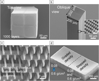
Figure 2 shows TPP-fabricated foams with different designs and made using IP-Dip photoresist. Reference Jiang, Campbell, Lu, Bernat and Petta43 The structure in Figure 2a is composed of four units of 100 × 100 µm2 foam printed adjacent to each other and stitched together at the interface. TPP fabrication was carried out by successively printing 50-µm-high subsections of each of the four units (Figure 2b). This was completed in a clockwise spiral until a final height of 1000 layers (1 mm) was reached. The quality of the stitching interface among the four columns is shown in Figure 2c. The designed horizontal and vertical offsets between the individual layers are clearly visible. Also, the interlacing of the layers extends 1 µm across the boundary of the two columns, based on these SEM images.
Basic foam structure composed of four individual 100 × 100 µm2 × 1-mm-high sections stitched together into a monolithic structure and shown in (a) top and (b) oblique views. (c) View of vertical stitched interface between the individual printed beams. (d) Foam structure fabricated by stitching together two sections, one with a graded density and the other with a stepped density. Reference Jiang, Campbell, Lu, Bernat and Petta43

Figure 2d shows a foam structure fabricated by stitching two sections of different density profiles. The graded density section has subblocks with dimensions of 0.1 × 0.1 × 0.15 mm3 and consists of 12 layers of woodpiles with densities ranging from 0.08 to 0.6 g/cm3. The stepped density section consists of two layers, 100- and 50-µm thick with densities of 0.08 and 0.6 g/cm3, respectively. In addition, shrinkage and deformation were observed following the development and drying of TPP. This is likely due to either incomplete photoreaction or solvent swelling of the polymer or both, especially on the density-varied foams. Initial attempts to control shrinkage by exchanging the developer with liquid CO2 followed by supercritical drying showed some improvement, but did not completely eliminate deformation.
With the demonstration of foam-like structure fabrication, TPP is expected to be extended to achieving FsLDW of millimeter to submillimeter prototypical structures with nanoscale accuracy and precision for broad applications (e.g., laser inertial fusion, micro-optics, cell culturing, and tissue engineering).
Fs laser assembly of aligned carbon nanotubes in three dimensions
Carbon nanotubes (CNTs) are a promising filler in polymer-based composites Reference Thostenson and Chou47 due to their remarkable mechanical, electrical, thermal, and optical properties; they have already demonstrated significant performance enhancement of polymer matrices. Reference Coleman, Khan, Blau and Gun’ko48–Reference Song, Zheng, Tang and Wang50 However, the functional effectivity of CNTs in composite materials strongly depends on the CNT weight percentage, dispersion, and displacement in the polymer matrix. Reference Park, Ounaies, Watson, Crooks, Smith, Lowther, Connell, Siochi, Harrison and Clair51 TPP-compatible resins with high CNT concentrations were developed for precise assembly of CNTs into 3D micro/nanostructures for functional device applications. Reference Xiong, Liu, Jiang, Zhou, Li, Jiang, Silvain and Lu52
The precise assembly of multiwalled carbon nanotubes (MWNTs) into 3D structures with controlled alignment was successfully achieved. Reference Xiong, Liu, Jiang, Zhou, Li, Jiang, Silvain and Lu52–Reference Ushiba, Shoji, Masui, Kono and Kawata54 The hybrid resins were prepared by directly adding acid-purified MWNT powders into TPP-compatible thiol-acrylate resins. Reference Xiong, Liu, Jiang, Zhou, Li, Jiang, Silvain and Lu52 With the additional advantage of TPP fabrication independent of the substrate, polyethylene terephthalate was used to demonstrate fabrication with MWNT thiol-acrylate (MTA) composite resins on flexible substrates.
In addition, strong anisotropic effects and precisely controlled MWNT assembly via FsLDW of MWNTs were observed. Good electrical and mechanical properties of the as-fabricated 3D micro/nanostructures were sequentially achieved. Raman spectroscopy confirmed that the MWNTs were indeed incorporated inside the as-fabricated microstructures. Reference Xiong, Liu, Jiang, Zhou, Li, Jiang, Silvain and Lu52 The characterization procedure for Raman spectroscopy of TPP microstructures can be found elsewhere. Reference Jiang, Zhou, Xiong, Gao, Huang, Jiang, Baldacchini, Silvain and Lu55 A comparison of Raman spectra of a composite with pure MWNTs showed a slight difference in line shape and blueshift of the MWNT G-band indicating thiol grafting of MWNTs in the composite resin. Reference Baskaran, Mays and Bratcher56,Reference Xu, Fang, Song and Peng57 The uniform distribution of MWNTs in the microstructure was shown by the Raman mapping image using G-band intensity mapping at each pixel.
The maximum MWNT concentration in MTA was reached at ∼0.2 wt%. To characterize the electrical conductivity of the MTA composites, two 5 × 5 × 75 µm3 (W × H × L, [W = width, H = height, L = length]) bar-shaped channels were made by TPP connecting two pairs of Au electrodes for electrical characterization. Both channels had the same geometry and were fabricated with the same writing parameters, but two different laser-scanning directions, either parallel with or perpendicular to the bar axis. The I–V (current–voltage) curves demonstrated that the channel fabricated using parallel scanning was 1000× more conductive than the channel fabricated using perpendicular scanning. The electrical conductance gap matched the high anisotropy in electrical conductivity of CNTs in directions parallel with or perpendicular to the CNT axis. Reference Borghese, Denti, Saija, Iati and Marago58 This indicates the strong orientation alignment of the MWNTs inside the polymer. Besides the enhancement of electrical conductivity, the loading of MWNTs was also found to significantly enhance the mechanical properties of the TPP-cured polymer structures (not shown here). The nanofabrication method can achieve controlled assembly of MWNTs in 3D micro/nanostructures, enabling a broad range of CNT applications, including 3D electronics, integrated photonics, and micro/nanoelectromechanical systems.
Multiphoton ablation of TPP polymerized microstructures
Multiphoton ablation (MPA) is another FsLDW technique established as a useful subtractive manufacturing technology in 3D micro/nanostructuring of solid materials by direct ablative writing. Reference Gomez, Tekniker, Goenaga, Lizuain and Ozaita59–Reference Xiong, Zhou, He, Gao, Mahjouri-Samani, Jiang, Baldacchini and Lu62 MPA requires simultaneous absorption of multiple photons in a single quantum event to initiate the ablation. Multiphoton absorption produces initial free electrons that are further accelerated by the fs laser electric field. These electrons induce avalanche ionization and optical breakdown and generate localized plasma. The subsequent expansion of the localized plasma results in the fabrication of a void structure at the focal point. Reference Chichkov, Momma, Nolte, von Alvensleben and Tunnermann63 Due to the nature of nonlinear interaction, high resolutions beyond the diffraction limit can be obtained.
A variety of micro/nanostructures have been fabricated by the MPA process. Chichkov et al. reported the fabrication of a photonic crystal structure with a defect cavity at the center by creating periodic nanostructures in sapphire using MPA. Reference Chichkov, Momma, Nolte, von Alvensleben and Tunnermann63 Sun et al. reported the fabrication of 3D photonic crystals within silica. Reference Sun, Xu, Juodkazis, Sun, Watanabe, Matsuo, Misawa and Nishii64 Zhou et al. fabricated the first void-dot, face-centered-cubic 3D photonic crystal in lithium niobate with a pronounced high-order stopgap at a wavelength of 1.5−2 µm. Reference Zhou and Gu65 It is noteworthy that thermal effects are almost negligible with minimum edge effects due to minimization of the fs pulse duration electron–photon interaction, ranging in the picosecond regime. Reference Korte, Serbin, Koch, Egbert, Fallnich, Ostendorf and Chichkov60 MPA is especially capable of fabricating structures such as channels, holes, and voids in various materials. Reference Gomez, Tekniker, Goenaga, Lizuain and Ozaita59–Reference Suriano, Kuznetsov, Eaton, Kiyan, Cerullo, Osellame, Chichkov, Levi and Turri61,Reference Zhou and Gu65–Reference Fischer, McWilliam, Paterson, Brown, Sibbett, Dholakia and MacDonald67
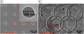
Figure 3a shows an array of holes created by MPA in an acrylic-based photoresist film (IP-L) that is 200 nm thick. Reference Xiong, Zhou, He, Gao, Mahjouri-Samani, Jiang, Baldacchini and Lu62,Reference Xiong, Zhou, Hou, Jiang, Mahjouri-Samani, Park, He, Gao, Fan and Baldacchini68 A magnified image of one hole is shown in the inset of Figure 3a, indicating a diameter of approximately 180 nm, far beyond the diffraction limit of the laser beam. In addition, Figure 3b shows five interconnected hollow rings created inside a cured IP-L polymer film. The channel width is 1 µm with sharp and clean ablation edges.
Micro/nanostructures fabricated by the subtractive multiphoton ablation (MPA) process in cured IP-L polymer films. (a) Scanning electron microscope micrograph of nanoholes; the inset is a magnified image of a hole with a sharp edge and a pore diameter of 180 nm; (b) optical image of five microsized interconnected hollow rings, resembling Olympic rings, embedded in a cured IP-L polymer film created by MPA. Reference Xiong, Zhou, He, Gao, Mahjouri-Samani, Jiang, Baldacchini and Lu62

Additive and subtractive micro/nanofabrication methods have been established separately, and they have been largely isolated from each other. Fabricating complex 3D geometries for advanced devices, such as a seamless spherical shell, calls for the use of both additive and subtractive processes, and such a comprehensive 3D micro/nanofabrication method possessing was sequentially developed. Reference Xiong, Zhou, He, Gao, Mahjouri-Samani, Jiang, Baldacchini and Lu62
The whole fabrication process consists of three steps. Reference Xiong, Zhou, Hou, Jiang, Mahjouri-Samani, Park, He, Gao, Fan and Baldacchini68 First, TPP was employed to create 3D solid microstructures inside the negative IP-L photoresist. Second, in the development process, unsolidified IP-L photoresist was washed away by a 20 min 99.5% isopropyl alcohol rinse. Third, a subtractive process based on MPA was carried out in air to tailor the cured IP-L to a desired 3D geometry. Writing in both additive and subtractive processes was achieved by moving the sample around a fixed laser beam by means of a computer-controlled X–Y–Z piezo stage. MPA typically requires an average laser power that is 2−7× higher than that used for TPP.
The capabilities of the “TPP + MPA” method were demonstrated by the following device structures. Figure 4 shows arrays of microstructured polymer fibers with different diameters. Reference Xiong, Zhou, He, Gao, Mahjouri-Samani, Jiang, Baldacchini and Lu62,Reference Xiong, Zhou, Hou, Jiang, Mahjouri-Samani, Park, He, Gao, Fan and Baldacchini68 The TPP process was employed to fabricate structures with 2, 1, and 0.5 µm linewidths (Figure 4a, c, and e, respectively). The laser average power and stage scanning speed employed for TPP were 7 mW and 100 µm/s, respectively. The different linewidths of the fibers were achieved by controlling the number of laser passes in fabricating a single polymer fiber. Upon polymerization, the refractive index of IP-L increased to a value of 1.52. Therefore, the polymer fibers could be used as light waveguides for integrated optics. Reference Zappe69 Following TPP, a subtractive MPA process was performed with a laser average power of 26 mW, a laser exposure time of 5 ms per spot, and a stage scanning speed of 100 µm/s. Periodic hole patterns ∼500 nm in diameter were fabricated along the polymer fibers to form Bragg grating structures in the waveguides, as shown in Figure 4b, d, and f. The diameter and the periodicity of the holes were tunable by adjusting the laser average power, exposure time, and scanning speed. It is noteworthy that the fiber Bragg gratings, as shown in Figure 4, are difficult to fabricate by either TPP or MPA alone.
Scanning electron microscope images of polymer fibers fabricated by the “TPP + MPA” method. (a), (c), and (e) Arrays of fibers created by TPP with 2, 1, and 0.5 μm diameters, respectively. (b), (d), and (f) Arrays of fibers with periodic hole patterns after the MPA process. Note: TPP, two-photon polymerization; MPA, multiphoton ablation. Reference Xiong, Zhou, He, Gao, Mahjouri-Samani, Jiang, Baldacchini and Lu62

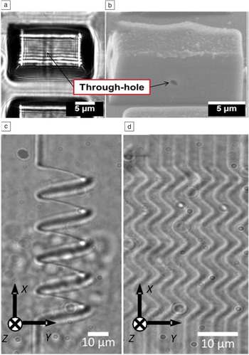
Another type of device structure is shown in Figure 5 , where straight (Figure 5a–b) and spiral microfluidic channel systems (Figure 5c–d) were fabricated, respectively. Liquid flowed through the meshed channels, which verified the hollow structure and the connectivity of the microfluidic channels. Reference Xiong, Zhou, He, Gao, Mahjouri-Samani, Jiang, Baldacchini and Lu62,Reference Xiong, Zhou, Hou, Jiang, Mahjouri-Samani, Park, He, Gao, Fan and Baldacchini68 The optical microscope image of the spiral channel changes as the focal plane of the observation shifts from low to high, as shown in Figure 5c, which indicates the 3D characteristics of the spiral microfluidic channel created inside the IP-L polymer. By using the “TPP + MPA” method, arrays of spiral microfluidic channels with user-defined spacing can be readily fabricated (Figure 5d).
2D microfluidic channels inside IP-L polymer fabricated by the “TPP + MPA” method. (a) Optical micrograph of a typical microfluidic channel inside a polymer cube; (b) Scanning electron microscope cross-section image of the microfluidic channel; (c) X–Y cross-sectional view of a spiral channel under a transmission-mode optical microscope; (d) Array of spiral microfluidic channels fabricated inside a polymer cube with a coil diameter of 5 µm and an interchannel spacing of 3 µm. Reference Xiong, Zhou, He, Gao, Mahjouri-Samani, Jiang, Baldacchini and Lu62

The structures previously described demonstrate the “TPP + MPA” method to be a promising technique for the fabrication of microvoids and microfluidic systems. The true 3D nature allows mask-free fabrication. The selective removal of polymer provides enhanced flexibility to make complex structures. High spatial resolution can be achieved with the nonlinear absorption process.
Three-dimensional glass micromachining with fs laser pulses
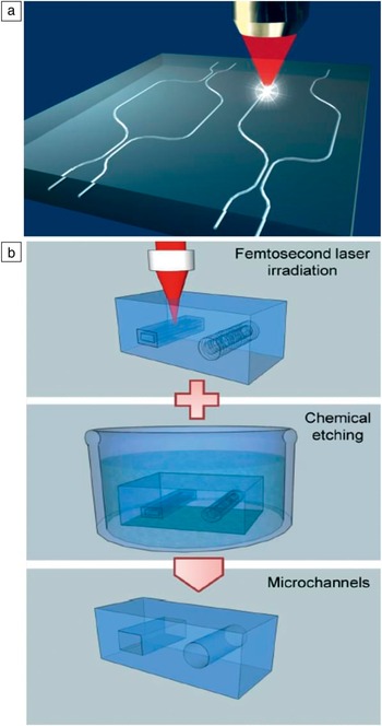
Fs laser pulses can also produce different types of modifications in glasses. Reference Hnatovsky, Taylor, Rajeev, Simova, Bhardwaj, Rayner and Corkum70 With low-fluence irradiation, a refractive-index variation is induced. With suitable sample translation, optical waveguides can be written within the volume of the glass ( Figure 6a). Reference Davis, Miura, Sugimoto and Hirao71,Reference Flamini, Magrini, Rab, Spagnolo, D’Ambrosio, Mataloni, Sciarrino, Zandrini, Crespi, Ramponi and Osellame72 With intermediate-fluence irradiation, nanogratings are created. Reference Shimotsuma, Kazansky, Qiu and Hirao73 Such nanostructures, oriented perpendicularly to the laser polarization, create anisotropic regions in otherwise isotropic glasses. These nanogratings have relevant applications to produce polarization-sensitive elements and microfluidic channels. The latter components require a two-step process (Figure 6b): (1) The material is irradiated to create the nanogratings in specific regions of the glass; and (2) chemical etching is used to selectively remove the irradiated regions, thus creating 3D cavities in the glass with arbitrary shapes. Reference Marcinkevicius, Juodkazis, Watanabe, Miwa, Matsuo, Misawa and Nishii74,Reference Paie, Bragheri, Vazquez and Osellame75 With high-fluence irradiation, microexplosions are produced, Reference Glezer and Mazur76 creating buried microvoids when focused in the volume of the glass, or material ablation when focused at the surface.
Femtosecond laser micromachining of glass. (a) Direct writing of 3D optical waveguide circuits. Reference Flamini, Magrini, Rab, Spagnolo, D’Ambrosio, Mataloni, Sciarrino, Zandrini, Crespi, Ramponi and Osellame72 (b) Fabrication of 3D microchannels with arbitrary cross sections: a first step of laser irradiation, according to the designed pattern, is followed by a second step of chemical etching to remove the irradiated material and finally produce the microchannels. Reference Paie, Bragheri, Vazquez and Osellame75

The versatility of fs laser micromachining enables application to many diverse fields. Direct writing of optical waveguides by this technique has been achieved in many different glasses, both doped and undoped. Reference Della Valle, Osellame and Laporta77 Waveguide lasers have been demonstrated in erbium-doped phosphate glasses, while passive components, encompassing couplers, interferometers, and Bragg filters have been produced in fused silica and borosilicate glasses. These components have found applications in devices for optical communications, Reference Eaton, Chen, Zhang, Iyer, Li, Ng, Ho, Aitchison and Herman78 integrated quantum optics, Reference Marshall, Politi, Matthews, Dekker, Ams, Withford and O’Brien79,Reference Sansoni, Sciarrino, Vallone, Mataloni, Crespi, Ramponi and Osellame80 and astrophotonics. Reference Thomson, Kar and Allington-Smith81 All of these devices took full advantage of the 3D capabilities of the FsLDW technique, which proved to be valuable in implementing new layouts that are not possible with standard 2D techniques. Examples are the interconnection between a one-dimensional fiber array and a 2D distribution of cores in a multicore fiber, Reference Thomson, Bookey, Psaila, Fender, Campbell, MacPherson, Barton, Reid and Kar82 as well as 3D directional couplers for polarization-insensitive operation. Reference Sansoni, Sciarrino, Vallone, Mataloni, Crespi, Ramponi and Osellame83
The possibility of direct writing nanogratings in glass, mainly fused silica, has also found many applications. Reference Beresna, Gecevicius and Kazansky84 Exploiting the strong birefringence created by the nanogratings, spatially varying waveplates have been produced to effectively generate complex polarization states of light. In addition, the formation of nanogratings at different depths has also enabled the demonstration of high-capacity optical read-only memories, where, besides the three spatial dimensions, the slow axis angle and retardance are also exploited to encode the information. As previously mentioned, the creation of a nanograting, followed by chemical etching, can also produce 3D microfluidic networks in glass. Reference Marcinkevicius, Juodkazis, Watanabe, Miwa, Matsuo, Misawa and Nishii74,Reference Cheng, Sugioka, Midorikawa, Masuda, Toyoda, Kawachi and Shihoyama85 This has been widely used for demonstrating 3D microfluidic and, in combination with optical waveguides fabricated by the same laser, optofluidic devices. Reference Osellame, Hoekstra, Cerullo and Pollnau86 The latter devices are particularly significant as they represent an example of how the synergistic combination of the different capabilities of fs material processing can enable the implementation of monolithic microsystems. Recent examples in this direction are optofluidic devices for cell manipulation Reference Paie, Bragheri, Vazquez and Osellame75,Reference Bragheri, Minzioni, Vazquez, Bellini, Paie, Mondello, Ramponi, Cristiani and Osellame87 and microorganism investigation. Reference Hanada, Sugioka, Shihira-Ishikawa, Kawano, Miyawaki and Midorikawa88,Reference Schaap, Rohrlack and Bellouard89
The third regime of laser–glass interaction, the one producing microexplosions, was initially proposed for high-density optical storage. Reference Glezer and Mazur76 Subsequently, it was also proposed to use this regime for water-assisted drilling to produce microfluidic channels, Reference An, Li, Dou, Liu, Yang and Gong90 although the resulting surface roughness of the microchannel inner walls is higher than what can be achieved with the etching-assisted two-step process previously described.
Summary
We have introduced the current developments in FsLDW for fabricating 3D micro/nanostructures in polymers and glasses. Studies were carried out to make large-dimension structures by TPP, fabricate electrical devices of MTA composite resins using TPP, simultaneously use TPP and MPA, and perform 3D micromachining (modification and ablation) of glass. The advantages associated with the nonlinear absorption process allow the precise, flexible, and efficient micro/nanofabrication of arbitrary 3D geometry in transparent materials. FsLDW of transparent materials is not limited to polymers and glasses; it can also be applied to crystals and a vast area of applications not addressed here. The rapid prototyping possibilities and versatility in processing different types of transparent materials are extremely valuable. This technology has enabled important scientific breakthroughs in academic research and is now becoming a viable industrial production process thanks to the many companies and startups that are adopting it.
Acknowledgments
The authors at the University of Nebraska–Lincoln would like to acknowledge financial support from the National Science Foundation (CMMI 1265122), Schafer Corporation, and Nebraska Center for Energy Sciences Research. R.O. acknowledges financial support from the European Union’s Horizon 2020 Research and Innovation Program under Grant No. 688510.

Li Jia Jiang is a postdoctoral research associate in the Laser Assisted Nano Engineering Lab in the Department of Electrical and Computer Engineering at the University of Nebraska–Lincoln (UNL). He obtained his BEng degree from Hefei University of Technology in 2008 and MEng degree from Dalian University of Technology in 2011, both in mechanical engineering. He earned his PhD degree in electrical engineering from UNL in 2016. His research interests include micro 3D printing, laser micromachining, nanomaterial growth, and mechanical design and fabrication. Jiang can be reached by phone at 402-472-3441 or by email at li.jia.jiang1985@gmail.com.

Shoji Maruo is a professor in the Department of Mechanical Engineering and Materials Science, Graduate School of Engineering, Yokohama National University, Japan. He received his BS degree in 1992, MS degree in 1994, and PhD degree in 1997, all in applied physics, from Osaka University, Japan. His research on two-photon 3D microfabrication has recently received considerable attention. His research interests include single-photon and two-photon microstereolithography, 3D ceramic moldings, lab-on-a-chip, MEMS, energy harvesting, and medical applications. Maruo can be reached by phone at +81-45-339-3880 or by email at maruo@ynu.ac.jp.

Roberto Osellame is a senior researcher at the Institute for Photonics and Nanotechnologies of the Italian National Research Council. He is also a professor at the Polytechnic University of Milan, teaching quantum optics and information. He received a PhD degree in physics from the Polytechnic University of Turin, Italy, and laurea degree in electronic engineering from the Polytechnic University of Milan. His research interests include the development of photonic circuits for quantum computing, the fabrication by two-photon-polymerization of micro/nanostructures of arbitrary geometry, and the integration of optical waveguides and microchannels for on-chip sensing in lab-on-a-chip and optofluidic manipulation of single cells. He is the author of more than 150 publications and holds six patents in the field of optics and photonics technology. Osellame can be reached by email at roberto.osellame@polimi.it.

Wei Xiong is a professor of optical and electrical information at Huazhong University of Science and Technology, China. He obtained his BSc degree from Huazhong University of Science and Technology in 2004 and MSc degree from Fudan University in 2007. He received his PhD degree in electrical engineering from the University of Nebraska–Lincoln in 2013. His research interests include synthesis and integration of carbon nanomaterials, such as carbon nanotubes and graphene, 3D fabrication of polymeric and carbon-based functional micro/nanostructures, and 3D micro/nanofabrication. Xiong can be reached by phone at +86-27 87485855 or by email at weixiong@hust.edu.cn.

John H. Campbell founded Material Science Solutions in 2007, a company specializing in advanced laser materials and materials processing research and development. Prior to this, he was a member of the senior scientific staff at Lawrence Livermore National Laboratory, where he developed optical materials for use on high-energy/high-peak-power lasers. He received his PhD degree in physical chemistry from the University of Illinois at Urbana-Champaign. He is a recipient of the International Otto-Schott Research Award for innovative research on glasses and glass ceramics in 1999, and the American Ceramic Society’s George Morey Award for research on laser glasses in 2003. He has received four R&D 100 Awards for inventions of new optical materials and processes. Campbell can be reached by phone at 925-784-5441 or by email at campbelljh@comcast.net.

Yong Feng Lu is the Lott Distinguished Professor of Engineering at the University of Nebraska–Lincoln (UNL). He received his bachelor’s degree from Tsinghua University, China, in 1984 and MSc and PhD degrees from Osaka University, Japan, in 1988 and 1991, all in electrical engineering. From 1991 to 2002, he was a member of the faculty in the Electrical and Computer Engineering Department at the National University of Singapore. He joined the Department of Electrical Engineering at UNL in 2002. His research interests include processing and characterization of micro/nanostructured materials. He has authored or co-authored more than 650 publications. He has been a SPIE Fellow, LIA Fellow, and OSA Fellow. Lu served as the president of the Laser Institute of America in 2014. Lu can be reached by phone at 402-472-8323 or by email at ylu2@unl.edu.