Introduction
In 2001, Nagamatsu et al.Reference Nakamatsu, Nakagawa, Muranaka, Zenitani and Akimitsu1 discovered that MgB2 was a superconductor with a surprisingly high transition temperature for a binary compound, T c = 40 K. Despite its conventional electron-phonon coupling mechanism, MgB2 was shown to possess two superconducting energy gaps originating in two different electron bands, σ and π, both of which cross the Fermi level, E F.
Since the beginning, a huge effort was expended to understand multiband effects in MgB2 and to explore its potential for affordable, dry applications of superconductivity. Because grain boundaries do not create serious weak links to reduce the critical current density (J c) in polycrystalline forms of the material,Reference Larbalestier, Cooley, Rikel, Polyanskii, Jiang, Patnaik, Cai, Feldmann, Gurevich, Squitieri, Naus, Eom, Hellstrom, Cava, Regan, Rogado, Hayward, He, Slusky, Khalifah, Inumaru and Haas2 long multifilamentary MgB2 wires with a relatively high J c of 105–106 A/cm2 were quickly manufactured by the scalable powder-in-tube (PIT) technique.Reference Grasso, Malagoli, Ferdeghini, Roncallo, Braccini, Siri and Cimberle3 These favorable characteristics yielded, less than 10 years after its discovery, commercial MRI systems based on MgB2 cooled by a cryo-generator, thus operating in a cryogen-free environment.
Further developments are now necessary to push the material toward high magnetic field applications, where superconductors have historically played a central role. Epitaxial MgB2 thin films exhibit much higher J c than polycrystals (by two orders of magnitude),Reference Eisterer4 very close to the depairing current density. Moreover, their upper critical magnetic field H c2 is near 60 T,Reference Braccini, Braccini, Gurevich, Giencke, Jewell, Eom, Larbalestier, Pogrebnyakov, Cui, Liu, Hu, Redwing, Li, Xi, Singh, Gandikota, Kim, Wilkens, Newman, Rowell, Moeckly, Ferrando, Tarantini, Marré, Putti, Ferdeghini, Vaglio and Haanappel5 which far exceeds the performance of industrial Nb-based superconductors currently used in virtually all commercial superconducting magnets. Unfortunately, these outstanding characteristics are far from being reached in polycrystalline MgB2 material forms, which suggests the presence of limiting factors for supercurrent transport that still need to be fully explained.
The article will review (1) the basic properties of MgB2, including its multiband nature, its two-gap superconductivity and critical parameters, and the ways in which these features affect the superconducting properties; (2) the superconducting properties, especially progress in understanding and improving the important upper critical field H c2, critical current density J c, vortex pinning, and connectivity; (3) development and fabrication of wires by ex situ and in situ manufacturing processes; and (4) existing and future applications, from medical devices to compact and efficient rotating machines.
Basic properties of MgB2
Multi-gap superconductivity was predicted since the 1950s,Reference Suhl, Matthias and Walker40 but MgB2 was the first clear example of a two-gap superconductor. The two-gap nature was pointed out immediately after the discovery of superconductivity in this compound, because it significantly affects the superconducting properties (for a review, see Reference Reference Xi6). It was observed that the T c value of 40 K was far too high to be explained within a conventional Bardeen-Cooper-Schrieffer (BCS) framework, and also H c2 was unusually high when compared to single-band superconductors. While the electronic specific heat showed a significant contribution at low temperatures due to quasiparticles excited above a small superconducting gap, clear signals of the two gaps were evident both in point-contact and tunneling measurements. Theoretical calculations quantitatively explained the observed anomalies and predicted novel two-gap effects. These developments provided an extraordinary example of the way that theory and experiments can proceed in parallel to achieve a satisfactory understanding of a new phenomenon.
The origin of two-gap superconductivity resides in the peculiar electronic structure of MgB2 (shown in Figure 1), which is characterized by two groups of bands. The σ bands arise from orbitals that are localized around the B planes and are hole-like, anisotropic, and strongly coupled with the E 2g optical mode of the B ions. The π bands are mainly electron-like, three-dimensional, and weakly coupled with phonons. Moreover, σ and π orbitals have different parity, so that interband scattering by impurities is largely suppressed. This is a crucial feature, because it means that scattering by impurities is not effective in mixing the weakly coupled and strongly coupled Cooper pairs that form in the two bands. Each band develops superconductivity with individual characteristics, and two perfectly separated gaps are clearly observable even in non-ideal samples. Table I shows these gaps for the two bands, as well as the values of superconductivity parameters, coherence length (ξ), penetration depth (λ), Ginzburg-Landau parameter (κ = λ/ξ), and ab-plane Fermi velocity (v Fab) and its anisotropy (v Fab/v Fc) for clean-limit samples.
The electronic structure of MgB2. The thick lines represent σ and π bands, crossing the Fermi level (horizontal dashed line). The inset shows the hexagonal crystallographic structure. Image courtesy of S. Massidda.

Characteristic properties of the σ and π bands.

Zero-temperature energy gap Δ(0), Fermi velocity in the ab-plane and its ratio to the perpendicular value, coherence length ξ and penetration depth λ, and their ratio κ. The Δ(0) values were determined experimentally, while the ξ values were estimated from the BCS expression  , and the λ values were deduced from the respective plasma frequencies.
As one can see from the Ginzburg-Landau parameters κ, clean MgB2 exhibits the unusual combination of being both a Type 1 (κπ < 1/√2) and a Type 2 (κσ > 1/√2) superconductor, the new term Type 1.5 superconductor being therefore coined for it.Reference Moshchalkov, Menghini, Nishio, Chen, Silhanek, Dao, Chibotaru, Zhigadlo and Karpinski7 This peculiarity is removed only by increasing structural disorder, although a clear distinction between the two bands still remains visible. Indeed, due to the negligible interband scattering, different types of impurities selectively affect the π and σ mean free paths with distinct consequences, especially for H c2 in the two principal directions.Reference Putti, Braccini, Ferdeghini, Pallecchi, Siri, Gatti, Manfrinetti and Palenzona8
The effect of impurities on T c is extremely peculiar in two-gap superconductors because, unlike in single-band superconductors, scattering by non-magnetic impurities breaks pairs and strongly suppresses T c. In the case of MgB2 it was predicted that, with increasing disorder, T c should saturate to 20 K, where an equivalent one-gap system stabilizes.Reference Dolgov, Kremer, Kortus, Golubov and Shulga41 However, given the previously mentioned fact that the symmetry of σ and π orbitals makes the interband scattering rate quite small even in rather dirty samples, many efforts have been carried out to verify this prediction. The effects of disorder have been extensively investigated, but only a few substitutions are successful. Among them, the most deeply investigated are the substitution of Al on the Mg site and C on the B site.
Both of these substitutions decrease T c. This can be understood mainly in terms of σ-band filling due to the electron doping by Al and C, which reduces the σ-band density of states (DOS).Reference Kortus, Dolgov, Kremer and Golubov9 On the other hand, Al and C influence the transport properties in different ways, with important consequences for H c2 that are described in the Tarantini and Gurevich article in this issue.
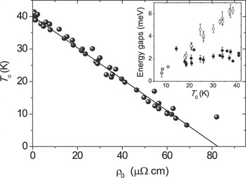
Neutron irradiation allows for the study of defects without doping the systemReference Putti, Vaglio and Rowell10 and has demonstrated how interband scattering suppresses T c and merges the two energy gaps. However, as is shown in Figure 2, the T c decrease does not saturate around 20 K, as expected for isotropic MgB2, but progressively decreases down to zero. This result demonstrates that intraband scattering causes smearing of the DOS and further diminishes T c by a similar mechanism to that previously observed in superconductors with the A15 structure, such as Nb3Sn.Reference Putti, Brotto, Monni, Galleani d’Agliano, Sanna and Massidda11 It is interesting that the σ DOS is suppressed more by scattering, because it becomes zero only 0.7 eV above E F. Thus the σ bands and their strong coupling with B vibrations, which are responsible for the high T c of MgB2, have an intrinsic weakness due to the proximity of the top edge of the band to the Fermi level. Thus doping and alloying have been less effective in improving the superconducting properties than in many superconducting systems.
Superconducting critical temperature T c of MgB2 as a function of the residual resistivity ρ0 of a collection of irradiated samples. Inset: the energy gaps Δσ (0) (empty symbols) and Δπ (0) (filled symbols) as a function of T c (see Reference Reference Putti, Vaglio and Rowell10).

Superconducting properties of MgB2
Making MgB2 suitable for power applications requires optimization of (1) the upper critical fields, (2) vortex pinning, and (3) intergranular connectivity, as summarized in the following sections and detailed in other reviews (References Reference Eisterer4 and Reference Collings, Sumption, Bhatia, Susner and Bohnenstiehl12).
Upper critical field
The zero-temperature upper critical field H c2 of clean MgB2 single crystals is strongly anisotropic and rather low, with  ∼3 T and
 ∼16 T, where the indices ⊥ and ‖ correspond to the magnetic field perpendicular and parallel to the ab-plane, respectively. The anisotropy
 ∼5 corresponds to the anisotropy of the Fermi velocity of the σ bands (see Table I).
As a rule, disorder causes H c2 to rapidly increase and the anisotropy to diminish (see the Tarantini and Gurevich article in this issue). This is most remarkable in thin films, where H c2 can exhibit significant positive curvature close to T c, then increase linearly with decreasing T, yielding low-temperature H c2(0) values up to 60 T. These peculiarities are consequences of the two-gap nature of MgB2 (see the Tarantini and Gurevich article in this issue for more details). The two-gap modelReference Gurevich13 explains the anomalous temperature dependence and enhanced H c2 of thin films on the assumption that π bands become dirtier than σ bands. Indeed, recently it has been shown that increasing the scattering rate of π bands can enhance H c2 without affecting T c. In contrast, large σ-band scattering, effectively increases H c2, but also suppresses T c by the mechanism described in the previous section.Reference Brotto, Pallecchi, Putti and Galleani D’Agliano14
This recipe of π-band dirtying seen in films to increase H c2 has not yet been successful in bulk materials such as wires and tapes,Reference Zhu, Zhu, Pogrebnyakov, Wilke, Chen, Xi, Redwing, Zhuang, Feng, Gan, Singh, Shen, Newman, Rowell, Hunte, Jaroszynski, Larbalestier, Baily, Balakirev and Voyles15 for which different forms of C-doping that mainly affect the σ-band proved to be more effective. Indeed H c2(0) values exceeding 30 T are obtained in C-doped MgB2 wiresReference Wilke, Bud’ko, Canfield, Finnemore, Suplinskas and Hannahs16 and in SiC-alloyed bulk samples,Reference Matsumoto, Kumakura, Kitaguchi, Senkowicz, Jewell, Hellstrom, Zhu, Voyles and Larbalestier17, Reference Sumption, Bhatia, Rindfleisch, Tomsic, Soltanian, Dou and Collings18 and record values above 40 T were reported for C-nanotube-doped samples.Reference Serquis, Serrano, Moreno, Civale, Maiorov, Balakirev and Jaime19
Vortex pinning
The critical current in a magnetic field B is determined by the pinning force F P = J cB that keeps vortices from moving. The pinning strength can be increased by increasing H c2, which makes the superconductor more resilient to the applied field. In addition, pinning is increased by including a fine dispersion of defects, whose separation should match the vortex spacing and whose size should be comparable with the coherence length.Reference Putti, Brotto, Monni, Galleani d’Agliano, Sanna and Massidda11 The best results are obtained by adding carbon in elemental form (microspheres, nanotubes, nanodiamond) or by C-containing compounds such as SiC, TiC, B4C, and organic compounds. Also nitrides, borides, and silicides as well as several metal oxides have been added, often yielding encouraging results.
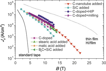
A collection of some of the best results obtained in the last few years, in comparison with a standard MgB2 tape without additions, is shown in Figure 3.Reference Matsumoto, Kumakura, Kitaguchi, Senkowicz, Jewell, Hellstrom, Zhu, Voyles and Larbalestier17, Reference Gao, Ma, Zhang, Wang, Yu, Watanabe, Yang and Wen20–Reference Matsumoto, Kobayashi, Takahashi, Kumakura and Kitaguchi26 It is very clear from this plot how essential it is to develop the highest possible H c2, because J c drops to zero as this field is approached. It is also important to improve the vortex pinning, which raises the local J c(H) slope, and to remove any current-limiting factors such as wetting phases on grain boundaries that can reduce the cross-section available for superconducting current and thus reduce the effective J c. These studies on real materials, especially on different forms of the conductor, are still in the early stages.
Critical current J c as a function of magnetic field B at 4.2 K for a standard MgB2 tape, improved samples with different types of additions,Reference Matsumoto, Kumakura, Kitaguchi, Senkowicz, Jewell, Hellstrom, Zhu, Voyles and Larbalestier17, Reference Gao, Ma, Zhang, Wang, Yu, Watanabe, Yang and Wen20–Reference Flukiger, Lezza, Cesaretti, Senatore and Gladyshevskii25 and a nanostructured thin film.Reference Matsumoto, Kobayashi, Takahashi, Kumakura and Kitaguchi26 (See references given for details about the different samples.)

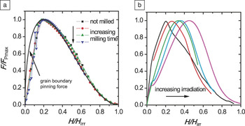
An important way to enhance J c(H) is by introducing dense, nanoscale defects. Despite many attempts at nanoparticle additions, the principal pinning defects in MgB2 are grain boundaries, which yield a pinning force F p=J cB, falls off rather rapidly as h 1/2(1–h)2, where h = H/H irr, and the irreversibility field H irr is the field at which J c = 0 (as shown in Figure 4a). Figure 4a shows the effect of ball milling, which reduces the grain size in the precursor powder and increases the grain-pinning. All the curves perfectly overlap the theoretical curve. Figure 4b shows the effects of neutron irradiation. In this case, the F p curves shift to larger h with increasing irradiation, providing one of the few clear examples in which point defects with appropriate size and spacing are homogeneously introduced and provide the expected significant enhancement of J c(H).Reference Tarantini, Aebersold, Bernini, Braccini, Ferdeghini, Gambardella, Lehmann, Manfrinetti, Palenzona, Pallecchi, Vignolo and Putti27
(a) Vortex-pinning force F P normalized to its maximum value F Pmax versus the reduced field h = H/H irr. The continuous line represents the theoretical expression for the normalized grain boundary pinning force. The experimental curves are measured in tapes produced by the ex situ powder-in-tube method and by varying the high-energy ball-milling time of the precursor powders. (b) F P/F Pmax for neutron irradiated polycrystalline samples.

To enhance grain-boundary pinning, a natural route is to decrease the grain size, for example by high-energy ball milling of the precursors,Reference Senkowicz, Mungall, Zhu, Jiang, Voyles, Hellstrom and Larbalestier28 and reducing the sintering temperature.Reference Romano, Vignolo, Braccini, Malagoli, Bernini, Tropeano, Fanciulli, Putti and Ferdeghini29 Up until now, nano-sized grains provided the highest J c values, as shown in Figure 3, where extremely large J c values exceeding 104 A/cm2 at 22 T are reported for MgB2 thin films with an H‖film.Reference Matsumoto, Kobayashi, Takahashi, Kumakura and Kitaguchi26 This exceptional result is achieved by  as large as 45 T and grains of 10–20 nm in size.
Connectivity
Compromised connectivity between superconducting regions is common to all polycrystalline forms of MgB2, even though this appears to be an extrinsic rather than an intrinsic weak-link limitation of J c in MgB2.Reference Braccini, Braccini, Gurevich, Giencke, Jewell, Eom, Larbalestier, Pogrebnyakov, Cui, Liu, Hu, Redwing, Li, Xi, Singh, Gandikota, Kim, Wilkens, Newman, Rowell, Moeckly, Ferrando, Tarantini, Marré, Putti, Ferdeghini, Vaglio and Haanappel5 RowellReference Rowell30 first recognized the possibility of a “cross-sectional deficiency” (reduced sample cross-section relative to the geometrical one) in polycrystals and suggested a general procedure for evaluating the effective cross-section factor, K, from simple electrical resistivity measurements as a function of temperature. For most polycrystals, K is on the order of 10% or less. Since the current flows through a smaller cross-section area, the intergrain J c is systematically underestimated by a factor of 10 or more (1/K). Indeed, J c (in a self-field at 5 K) of polycrystalline materials does not exceed 105–106 A/cm2, while much larger values of the order of 107–108 A/cm2 are achieved in fully connected, single crystal thin films.Reference Eisterer4 However, the reduced cross-sectional area cannot be the only factor that limits J c in randomly oriented polycrystals, because even fully connected materials (K∼1) have J c < 106 A/cm2.Reference Tarantini, Aebersold, Bernini, Braccini, Ferdeghini, Gambardella, Lehmann, Manfrinetti, Palenzona, Pallecchi, Vignolo and Putti27
Multiple factors can reduce K. First, due to poor sintering and the reduction of volume that occur when Mg and B powders are reacted, the typical density in MgB2 bulk samples, wires, and tapes is as low as 50% of the theoretical value (2.62 g·cm−3).Reference Yamamoto, Shimoyama, Kishio and Matsushita31 It is also well recognized that the surface of grains of MgB2 is easily covered by insulating oxide layers, such as MgO or amorphous BOx. Additional subtle effects may arise from the H c2 anisotropy, which controls J c(H) as current meanders between randomly oriented and perhaps imperfectly connected grains. The supercurrent carried by π Cooper pairs is isotropic and can freely move across misaligned grains, but it is strongly affected by temperature and the magnetic field. In contrast, the supercurrent carried by σ bands is less sensitive to temperature and field but is strongly anisotropic.
In order to increase the connectivity, a number of strategies have been pursued: improving density by the application of external pressure during synthesis; limiting impurity phases at grain boundaries by using high purity precursors and avoiding dopants; limiting the formation of MgO layers by carrying on the process in inert atmosphere; increasing grain size in order to reduce the exposed and perhaps contaminated grain surfaces; and texturing MgB2 by mechanical means or under a magnetic field.Reference Yamamoto, Shimoyama, Kishio and Matsushita31–Reference Vignolo, Romano, Malagoli, Braccini, Tropeano, Bellingeri, Fanciulli, Bernini, Honkimaki, Putti and Ferdeghini33 This suggests that the optimization of the process for producing outstanding MgB2 conductors should be selected considering the prerequisites of the specific application under study.
MgB2 wires
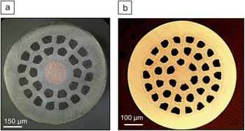
The powder-in-tube method (PIT) was almost immediately identified as a route to long MgB2 wires.Reference Grasso, Malagoli, Ferdeghini, Roncallo, Braccini, Siri and Cimberle3, Reference Jin, Mavoori, Bower and van Dover34 In this process, either pre-reacted MgB2 (ex situ) or Mg and B precursors (in situ) is packed inside a workable metallic tube, followed by mechanical deformation. Annealing steps can be applied during, as well as after, deformation in order to react the phase, to sinter it, or to release deformation stresses. Multifilamentary architectures can be achieved by restacking monofilament elements, as is shown in Figure 5, where both ex situ Reference Braccini, Nardelli, Penco and Grasso24 (Figure 5a) and in situ Reference Tomsic, Rindfleisch, Yue, McFadden, Doll, Phillips, Sumption, Bhatia, Bohnenstiehl and Collings35 conductors (Figure 5b) are shown.
(a) Transverse cross-section of an ex situ MgB2 wire. (Image courtesy of Columbus Superconductor.) (b) Transverse cross-section of an in situ MgB2 wire. (Image courtesy of Hypertech Research.)

Ex situ processing is technically more complex, since it requires an additional reaction step before wire formation and subsequent powder handling in inert atmosphere to avoid significant MgB2 surface passivation and degradation of connectivity. A short heat treatment above 900°C is required to sinter the MgB2 particles at the final wire size. Hard sheaths of nickel, iron, or titanium alloys favor a high packing density of the MgB2 powder, better connectivity, and higher mechanical strength.
By contrast, in situ wires are less sensitive to manufacturing parameters, since conductor fabrication occurs with unreacted precursors. Thanks to heavy mechanical processing, the precursors become more reactive, so reaction to MgB2 occurs between 600°C and 700°C, allowing finer grains and more lattice defects and better J c(H) behavior. The main drawbacks are low MgB2 density and reduced mechanical strength and homogeneity over long lengths, which result from the volume expansion of the Mg + B reaction.
However, both methods have proven the feasibility of fabrication of multi-km-long superconducting wires, whose properties have been successfully demonstrated in a number of magnets, cables, and other devices. Both types of wires are now able to carry, over a long length, J c exceeding 200,000 A/cm2 in the superconductor at 20 K in a magnetic field of 1 Tesla, with a fractional MgB2 cross-section of 15–30%.
Applications
The availability of long MgB2 wires, produced soon after the discovery of MgB2 as a superconductor, allowed for a number of demonstrators and, lately, of the first commercial product. A vital part of this development has also been the understanding that MgB2 is potentially highly cost-effective.
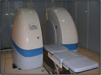
Among the most innovative developments, the open-MRI system, developed by ASG Superconductors and Paramed, is one of the most direct examples (Figure 6).Reference Razeti, Angius, Bertora, Damiani, Marabotto, Modica, Nardelli, Perrella and Tassisto36 Without any liquid cryogens (i.e., dry), a U-shaped open magnet system uses 18 km of ex situ MgB2 tape at 20 K to produce a magnetic field of 0.5 Tesla within a patient-accessible bore of about 60 cm. The peak magnetic field on the conductor is about 1.2 Tesla. A picture of the commercial system is shown in Figure 6. MRI magnet development was also carried out with in situ MgB2 wire in a more standard solenoid configuration.Reference Yao, Bascun, Kim, Hahn, Lee and Iwasa37
First commercial MgB2-based MRI system. (Image courtesy of ASG Superconductors.)

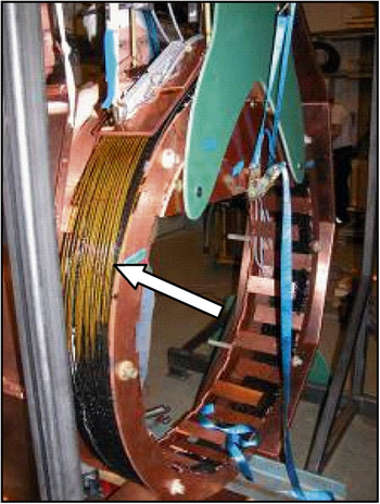
In another development at Tampere University of Technology, dry MgB2 coils have also been applied to the highly energy-efficient induction heating of large copper and aluminum billets prior to their extrusion.Reference Magnusson and Runde38, Reference Stenvall, Magnusson, Jelinek, Grasso, Hiltunen, Korpela, Lehtonen, Mikkonen and Runde39 Like the MRI magnet, the coil uses several km of wire and is shown in Figure 7 before being encased in its vacuum chamber.
Induction heater MgB2 coil (indicated by the arrow) prior to insertion in its vacuum chamber for testing.

Other successful demonstrations of MgB2-based devices have been carried out worldwide, from fault-current limiters to generators, transformers, superconducting magnetic energy storage systems, and dc cables. Collectively, these demonstrations show both the great appeal and the diversity of application of the material, which surely has a bright potential, not least because of its affordable cost/performance ratio and its commercial availability in lengths of more than 1 km.
Summary
Ten years after their discovery, the superconducting properties of MgB2 have been extensively investigated and understood in their main aspects. Impressive improvements have been achieved by making conductors with useful J c(H) characteristics that permit applications, for example to MRI systems in cryogen-free environments where Nb-based materials cannot operate. A number of demonstrations, such as fault-current limiters, generators, transformers, superconducting magnetic energy storage systems, and dc cables, have further shown the potential of this recently discovered superconductor.
This article reviewed this exciting adventure, underlining the still unclear features, the aspects that need further improvement, and the achievable objectives in order to push MgB2 toward an even brighter future in new application domains.