I. INTRODUCTION
Inductive power transfer (IPT) enables the operation of many implantable medical devices that are space limited or require long-term power draws that are too large for batteries to be appropriate. Example applications include neural recording [Reference Mestais, Charvet, Sauter-Starace, Foerster, Ratel and Benabid1], neural stimulation [Reference Ghovanloo and Najafi2], and hydrocephalus monitoring [Reference Hu, You, Chen, McCormick and Budgett3]. An IPT power supply typically uses a primary pickup to generate a time varying magnetic field that can pass through the skin. The magnetic field interacts with a secondary coil implanted below the skin inducing an AC voltage. A rectifier can convert the AC voltage into a DC supply to power an implanted device. A key concern for wirelessly powered implanted medical systems is heating as elevated temperatures above 42 °C maintained over long periods can lead to tissue damage [Reference Gowrishankar, Stewart, Martin and Weaver4, Reference Fujii and Ibata5]. Research groups have reported small integrated circuit rectifiers with efficiencies above 90% [Reference Bawa and Ghovanloo6–Reference Park9]. However, losses within the secondary pickup are also of great interest as these will be translated into heat [Reference Leung, Budgett and Hu10] and can be larger than the rectification losses.
Typically, an IPT circuit is impedance matched with the load for maximum power transfer capability, maximum efficiency or a compromise between the two. Often, to reduce heating within the body, the power efficiency at the secondary side of an IPT system has a much higher priority than efficiency at the primary side. Thus, the IPT system may be designed to maximize the efficiency of the secondary power pickup as opposed to the system as a whole.
Maintaining a constant output voltage against changes in the load and magnetic coupling variation is another major challenge in IPT system design. This can be achieved using a wireless feedback loop that adjusts the primary field strength based on the secondary output voltage [Reference Si, Hu, Malpas and Budgett11, Reference Dissanayake12]. However, it would be desirable to have power flow control implemented independent of the primary in situations such as multiple power pickups with one primary or as a system failsafe solution. Decoupling control is a method of achieving this [Reference Covic and Boys13–Reference Boys and Covic15]. In this paper, a traditional decoupling method, referred to as shorting control (SC), is integrated into a complementary metal-oxide-semiconductor (CMOS) synchronous rectifier to regulate the power flow and keep the output voltage constant under variable magnetic coupling conditions. Previous integrated circuit rectifiers have used capacitors to detune the resonant pickup for over-voltage protection but have not considered their use for power flow control or their effect on pickup efficiency [Reference Lee and Ghovanloo16–Reference Kiani, Lee, Yeon and Ghovanloo18]. Reconfigurable voltage rectifiers (1x/2x) can maintain load voltage with reduced open-circuit voltage [Reference Li, Tsui and Ki19, Reference Lu, Li, Ki, Tsui and Yue20], but cannot maintain a constant output voltage with increased open-circuit voltage. A recent “Q-modulation” technique has been used to maintain high power transfer efficiency by chopping the pickup with a low-loss switch every half cycle of the power carrier [Reference Kiani, Lee, Yeon and Ghovanloo18]. This technique has been used for series tuned pickups and increases the efficiency of the IPT link as opposed to the secondary pickup efficiency. This method does not regulate the load voltage. Compared with previous techniques used with integrated circuits, SC can be implemented in an integrated circuit with no additional external components, is used with parallel tuned secondary pickups and can maintain constant load power and voltage over a wide range of open-circuit voltages. The effective load resistance is dynamically changed by SC so that the secondary power pickup moves away from the maximum power matching at low coupling and towards a higher efficiency operation with increased coupling while still providing the required output power.
The efficiency and load power of a parallel tuned pickup with load resistance are analyzed in Section II. Section III describes the implementation of SC within a CMOS synchronous rectifier. A novel analysis is completed in Section IV describing the change in secondary pickup efficiency with the duty ratio of the SC scheme. Experimental results validating the analysis are presented in Section V and conclusions in Section VI.
II. PARALLEL TUNED SECONDARY PICKUP
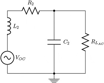
A parallel tuned pickup was used as it generates a constant current source, which can be used to increase the output voltage to be higher than the induced voltage in the power pickup coil [Reference Covic and Boys13, Reference McCormick21], and is hence a desirable tuning method for implantable devices where weak and fluctuating magnetic coupling is expected. The root mean square (RMS) voltage induced in the secondary coil of an IPT power pickup as shown in Fig. 1 is V OC = jωMI 1 where ω is the angular frequency, M is the mutual inductance, and I 1 is the RMS current in the primary coil of the IPT system. Assuming the inductive link is loosely coupled, the secondary has a negligible effect on the primary [Reference Lenaerts and Puers22]. The pickup is normally designed to resonate at the wireless power-operating frequency. A parallel tuned pickup as seen in Fig. 1 has a resonant frequency of,
 $$\omega _0 = \sqrt {1/(C_2 L_2 ) - 1/(C_2^2 R_{L_{{\rm AC}}} ^2 )}, $$
where L
2 is the pickup inductance, C
2 is the resonant capacitance, and
 $R_{L_{{\rm AC}}} $
is the equivalent AC load resistance. When
 $R_{L_{{\rm AC}}} \gg \; \sqrt {L_2 /C_2} $
equation (1) can be approximated to
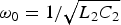 $\omega _0 = 1/\sqrt {L_2 C_2} $
, the normal condition for resonance. The pickup is designed to match with the load for maximum power transfer, maximum efficiency, or a compromise between the two.
Parallel tuned inductive power transfer pickup with resonant capacitor.

The power output to the equivalent AC load resistance can be calculated from Fig. 1 to be,
 $$P_{R_L} = V_{{\rm OC}}^2 \displaystyle{{R_{L_{{\rm AC}}}} \over {R_2^2 + (\omega _0 L_2 + R_{L_{{\rm AC}}} /Q_2 )^2}} $$
where V OC is the RMS open-circuit voltage, Q 2 = ω0 L 2/R 2, and R 2 is the equivalent series resistance (ESR) of the pickup coil. The power dissipated in the coil ESR can be found from,
 $$P_{R_2} = V_{{\rm OC}}^2 \displaystyle{{R_2 (\omega _0^2 L_2^2 + (R_L + R_2 + R_L^2 /(Q_2^2 R_2 ))^2 )} \over {(R_2^2 + (\omega _0 L_2 + R_{L_{{\rm AC}}} /Q_2 )^2 )^2}}. $$
The secondary pickup efficiency is of great importance because the secondary heating is more concerning than the primary heating for biomedical applications with impalpable devices. Assuming losses in the tuning capacitor are negligible, the secondary pickup efficiency is defined as,
 $$\eta _2 = P_{R_{L_{{\rm AC}}}} /\left( {P_{R_{L_{{\rm AC}}}} + P_{R_2}} \right).$$
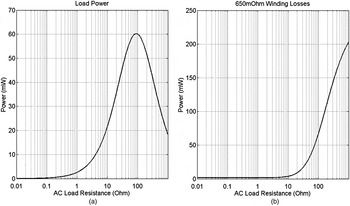
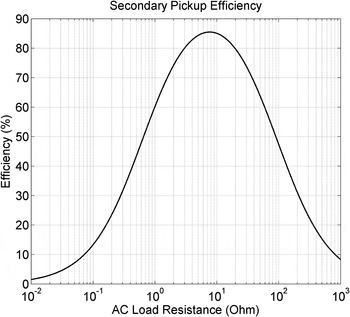
The pickup parameters were measured from a fabricated coil having inductance L 2 = 2 µH and resistance R 2 = 0.65 Ω. A secondary capacitor with C 2 = 35 nF was used to obtain a resonant frequency of 600 kHz. A plot of the load power and winding losses is shown in Figs 2(a) and 2(b), respectively, for an open-circuit voltage of 0.56 V. It can be seen that maximum power transfer to the load occurs with a 90 Ω AC load. The secondary coil losses are equal to the load power at this point and increase with larger loads. For this pickup, the maximum secondary pickup efficiency occurs at an AC load resistance approximately an order of magnitude lower than that corresponding to maximum power transfer as seen in Fig. 3. The bell shaped power efficiency curve can be explained by looking at the two extremes of zero load resistance and infinite load resistance. When C 2 is short circuited, all of the power is lost in R 2; and when the circuit is open with an infinite load resistance, no current flows through the load. Again, all power is lost in R 2. Both cases lead to zero power transfer efficiency.
(a) Load power and (b) secondary winding losses for a parallel tuned pickup matched to an 90 Ω load for maximum power transfer. The open-circuit voltage V OC is 0.56 V.

Secondary pickup efficiency for parallel tuned pickup matched to a 90 Ω load for maximum power transfer. The voltage V OC is 0.56 V.

III. CMOS IMPLEMENTATION
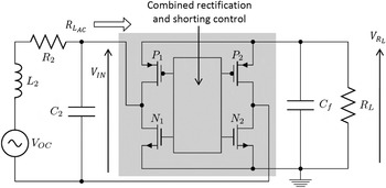
An integrated synchronous rectifier implemented in CMOS similar to [Reference Bawa and Ghovanloo6] was used for experimental validation of SC. The rectifier uses zero voltage switching of the bridge transistors and is approximately 90% efficient with output powers from 500 to 500 mW. The performance was validated using a similar setup as in [Reference Bawa and Ghovanloo6] and [Reference Lu and Ki7]. The control circuitry in Fig. 4 turns the transistors on and off at the correct instants to achieve rectification. The power transistors, rectifier control circuitry, and shorting controller are all integrated into a single IC. A second filter inductor after the rectifier is often used with traditional parallel tuned pickups as it smoothes the output current and improves the switching condition [Reference Si and Hu23]. However, due to the size limitations and inherent MRI compatibility requirements of implantable devices [Reference Stehlin, McCormick, Malpas, Pontré, Heppner and Budgett24], the second inductor at the DC side of the circuit is not preferred as it would increase the size of the pickup circuit, or cause ferromagnetic compatibility issues.
Rectifier and SC circuit. Grey box indicates the components integrated on chip. N 1 and N 2 act as the SC switches in addition to rectifier switches.

When the load voltage reaches V
th+ the controller connects the p-channel metal-oxide semiconductor (PMOS) rectifying transistor gates to
 $V_{R_L} $
switching them off and decoupling the load from the pickup. The n-channel metal-oxide semiconductor (NMOS) gates are also attached to
 $V_{R_L} $
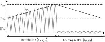
shorting the pickup to ground. The pickup input voltage and load voltage waveforms can be seen in Fig. 5. A soft turn on is used to reduce the peak current from the pickup tuning capacitor. The NMOS transistors have a combined resistance of 200 mΩ in the designed IC and the combined resistance becomes attached to the pickup in place of the load. The resonant capacitor is effectively shorted and the maximum current is limited by the inductance of the pickup coil. From Fig. 2, it can be seen that very little power is dissipated in the NMOS transistors (now the load) or the ESR of the pickup coil. Once
 $V_{R_L} $
drops back to V
th−, SC is disabled and rectification continues. This is an asynchronous form of control with no clocking and gives the minimum number of SC switch activations possible. If C
f is sufficiently large, the duration the shorting switch is active will contain many IPT periods, and the transient losses from discharging C
2 become negligible. V
th+ was designed to be 3.55 V and V
th− to be 3.35 V giving an approximate average output voltage of 3.45 V.
Input voltage and load voltage waveforms under rectification and SC. When V
th+ −V
th− is small,
 $V_{R_L} $
can be approximated to a DC voltage
 $V_{R_L} $
.

IV. SC ANALYSIS
The duration the SC switches are open with respect to closed can be found from the time it takes to charge and discharge the load capacitor. The off duration for the SC switches t SC,off can be approximated to,
 $$t_{{\rm SC,off}} = \displaystyle{{C_{\rm f} V_{\rm H}} \over {(I_{{\rm out,off}} - I_{R_L} )}},$$
where C
f is the filter capacitance, V
H = V
th+ − V
th− is the SC hysteresis, I
out,off is the average rectifier output current, while the pickup is not shorted and
 $I_{R_L} $
is the mean load current. The on duration for the SC switches is the time to discharge the capacitor,
 $$t_{{\rm SC,on}} = \displaystyle{{C_{\rm f} V_{\rm H}} \over {I_{R_L}}}. $$
SC maintains approximately constant load voltage and hence
 $I_{R_L} $
, the SC on time t
SC,on is also constant. Selecting C
f of appropriate size ensures t
SC,on is much longer than the IPT period. The off to on duty ratio for SC is then,
 $$D = \displaystyle{{t_{{\rm SC,off}}} \over {t_{{\rm SC,on}} + t_{{\rm SC,off}}}} = \displaystyle{{I_{R_L}} \over {I_{{\rm out,off}}}}. $$
The duty ratio represents the proportion of time the pickup is not shorted and the rectifier is active. As the output current from the rectifier increases relative to the load current, the pickup is shorted more frequently and for a longer period, rectification is active less and the duty ratio decreases.
For a fixed load, maintaining a constant output voltage with SC also maintains a constant output current. Therefore, the mean load current is,
 $$I_{R_L} = V_{R_L} /R_L. $$
As no current is delivered to the load and filter capacitor while the pickup is shorted, the rectifier output current during rectification has to be greater than the average load current. Substituting (7) into (8) and rearranging gives,
 $$I_{{\rm out,off}} = V_{R_L} /(DR_L ) = V_{R_L} /R_L^{\rm ^{\prime}}. $$
The effective AC load is smaller than the effective DC load by the impedance transform ratio of the rectifier α,
 $$R_{L_{\rm AC}} = \alpha R_L^{\prime} \therefore I_{{\rm out,off}} = \alpha V_{R_L} /R_{L_{{\rm AC}}}. $$
While rectification is active, I
out,off
in (10) can be substituted into (2) as
 $P_{R_L} = \alpha V_{R_L} ^2 /R_{L_{{\rm AC}}} $
resulting in,
 $$\displaystyle{{\alpha V_{R_L} ^2} \over {R_{L_{{\rm AC}}}}} = \displaystyle{{V_{{\rm OC}}^2 R_{L_{{\rm AC}}}} \over {R_2^2 + (\omega _0 L_2 + R_{L_{{\rm AC}}} /Q_2 )^2}}. $$
Rearranging and solving for
 $R_{L_{AC}} $
gives a definition in terms of V
OC,
 $$\eqalign{R_{L_{{\rm AC}}} & = \displaystyle{{\alpha V_{R_L} ^2 R_2} \over {\alpha V_{R_L} ^2 /{\rm Q}_2^2 - V_{{\rm OC}}^{\rm 2}}} \cr & \quad \left( {1 + \sqrt {1 - \displaystyle{{(\alpha V_{R_L} ^2 /{\rm Q}_2^2 - V_{{\rm OC}}^2 )(R_2 + {\rm \omega} _0^2 L_2^2 )} \over {\alpha V_{R_L} ^2 R_2^2}}}} \right).} $$
 $P_{R_L} $
and
 $P_{R_2} $
can then be found by substituting (12) back into (2) and (3). To simplify the following analysis, α = η
rec 0.5 is approximated where η
rec is the rectifier efficiency. This assumption is derived with the equivalence,
 $$\eqalign{& P_{R_L, {\rm DC}} = \eta _{{\rm rec}} P_{R_L, {\rm AC}} \therefore \displaystyle{{V_{R_L, {\rm DC}}^2} \over {R_L}} = \eta _{{\rm rec}} \displaystyle{{V_{R_L, {\rm AC}}^2} \over {R_{L_{{\rm AC}}}}} \cr & \quad \to R_{L_{{\rm AC}}} = \eta _{{\rm rec}} \displaystyle{{V_{R_L, {\rm AC(peak})}^2} \over {2V_{R_L, {\rm DC}}^2}} R_L.} $$
If the voltage drop across the rectifier is small, V R L ,AC(peak) ≈ V R L ,DC and the approximation is justified.
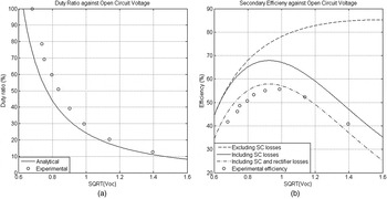
An increase in V OC decreases the effective load seen by the pickup. This load decrease shifts the secondary matching from maximum power transfer towards maximum efficiency. Ideally, zero power would be dissipated while the SC switches are on resulting in the dashed efficiency curve presented in Fig. 6(b). As the effective load drops, the efficiency increases until maximum efficiency is reached. This is consistent with the efficiency curve shown in Fig. 3. In practice, some power is dissipated during SC and depends on the duty ratio.
(a) Analytical and experimental duty ratio with square root of open-circuit voltage and (b) efficiency of the power pickup including and excluding losses during SC. The analytical effective load is proportional to the rectifier duty ratio.

The average load power
 $P_{R_L} $
will be constant regardless of the duty ratio as the load voltage is regulated. Ignoring rectifier losses, the total efficiency of the secondary pickup with SC is,
 $$\eta = \displaystyle{{P_{R_L}} \over {(P_{R_L} + P_{{\rm R}_2 {\rm, off}} D + P_{{\rm SC}} (1 - D))}},$$
where P R 2 ,off is the coil loss during rectification and P SC is the total power loss during SC including coil ESR and shorting switch losses. These can be calculated from (2) and (3). The SC duty ratio and secondary side efficiency with SC are shown in Fig. 6 for a 90 Ω AC load. With a 100% duty ratio, SC is never active, so the effective load is the real 90 Ω AC load. As the open-circuit voltage increases, the duty ratio decreases and the effective load drops. The change in effective load moves the operating point away from the maximum power point and towards the maximum efficiency point. SC losses affect the efficiency most at low duty ratios causing it to deviate from the ideal efficiency curve. This is intuitive as the output power will remain constant as V OC increases, but the SC losses will be larger and present for a greater proportion of the duty period.
V. EXPERIMENTAL RESULTS
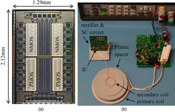
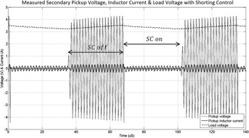
A CMOS synchronous rectifier shown in Fig. 7(a) with integrated SC was designed and fabricated to test the effectiveness of SC as a method of maintaining the highest available secondary pickup efficiency with the given coupling. The pickup was matched to a 90 Ω AC load at 600 kHz with the earlier pickup parameters L 2 = 2 µH, C 2 = 35 nH, and R 2 = 0.65Ω. A 4.7 µF filter capacitor was used at the output of the rectifier with a 200 Ω DC load (approximately 90 Ω AC with rectifier losses). As seen in Fig. 8, the discharge time from 3.55 to 3.35 V with SC active was 36 µS, approximately 20 times longer than the IPT period. The primary coil was larger than the secondary as seen in Fig. 7(b) helping ensure a loosely coupled system. The primary coil used an air core and had and outer coil diameters of 72 mm with three turns. The secondary used an air core coil with a 19 mm outer diameter having eight turns. A constant RMS current in the primary coil maintained a constant magnetic field distribution. The SC duty ratio was varied by decreasing the air gap between the primary and secondary coils to increase magnetic field coupling. The open-circuit voltage, secondary input power from the coil, winding losses, and power to the load were measured with different SC duty ratios.
(a) Integrated circuit with white boxes indicating transistors. (b) Experimental setup with large primary coil relative to secondary coil. Probes removed for clarity.

Measured secondary pickup voltage, inductor current and load voltage. SC was running with approximately 50% duty ratio.

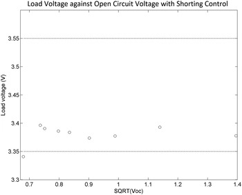
The average load voltage after the rectifier and SC was measured over a rage of open-circuit voltages and is presented in Fig. 9. Excluding the first measurement, all measured output voltages are within the hysteresis bands of the SC scheme. The open-circuit voltage is not large enough to create a load voltage above 3.35 V for the first data point.
Load voltage after rectifier with SC over a range of open-circuit voltages.

The efficiency of the power pickup, including the rectifier and SC circuitry, was calculated, and the results are presented in Fig. 6 against the simulation results. As the experimental AC load is not exactly 90 Ω, there are some small differences between the experimental and analytical results. At the minimum open-circuit voltage of 0.46 V, the duty ratio is 100% and the measured secondary efficiency is 42%. The maximum efficiency of 56% is reached with a V OC = 0.98 V, at which point the duty ratio is 30%. This relates to a 14% increase in efficiency with an approximate 100% increase in coupling. As expected from the analytical results, efficiency begins to decrease past this point due to losses in the SC transistors and inductor ESR. The losses within the rectifier are not accounted for within the analytical calculation resulting in an offset between the experimental and analytical results. By adding the rectifier loss to the analytical curve a more direct comparison can be made with the experimental results. The results match the theory closely.
The proposed SC scheme is compared with existing integrated circuit over-voltage protection, voltage regulation, and power-flow control strategies in Table 1. All previous solutions require an additional detuning capacitor for over-voltage protection. This work utilizes SC for over-voltage protection, voltage regulation, and load matching with no additional chip components. To the knowledge of the authors, this work is the only IC designed to maximize secondary pickup efficiency from the secondary side and hence minimize secondary pickup losses. This is an important design requirement for implantable devices where secondary pickup efficiency is more important than system efficiency in minimizing device heating.
Comparison with recent integrated circuit power management strategies.

VI. CONCLUSIONS
A synchronous rectifier with integrated SC has been designed and fabricated for wireless power supply to biomedical implants. SC is used for power flow control output voltage regulation and over-voltage protection. A novel analytical solution describing how the proposed SC strategy changes the secondary pickup efficiency has been derived and validated experimentally. The change in the load allows the secondary to operate at a high efficiency, while maintaining the required output power as the coupling increases. A 14% increase in efficiency is gained when the duty ratio changes from 100 to 30% due to a increase in the open-circuit voltage from 0.46 to 0.98 V.
FINANCIAL SUPPORT
This work was supported by a Faculty Research Development Fund from the University of Auckland (grant number 3704603) and by the Ministry of Business, Innovation and Employment (grant number CONT-38565-SIP2), New Zealand.
 Robert Gallichan graduated with a B.E. (Hons.) degree in Electrical and Electronic Engineering from The University of Auckland, Auckland, New Zealand, in 2013. He is currently pursuing a Ph.D. with the Auckland Bioengineering Institute. His current research interests include combining inductive power transfer and integrated circuits to improve active implantable devices.
 Ho Yan (Alex) Leung graduated from the University of Auckland with a Bachelor of Engineering in Electrical and Electronic Engineering in 2009. He commenced a Ph.D. in Biomedical Engineering at the Auckland Bioengineering Institute in 2010 under the supervision of Associate Professors David Budgett and Patrick Hu. His Ph.D. project focused on the energy management and optimisation of Transcutaneous Energy Transfer (TET) systems for implantable heart pumps. Following the completion of his thesis at the end of 2013, Alex joined the ABI staff as a Research Fellow, developing systems to power implantable devices.
 David M. Budgett (M'09) received the Ph.D. degree in biomedical engineering from Imperial College London, London, UK., in 1995. He has held academic positions with the University of Sussex, Brighton, UK., and The University of Auckland, Auckland, New Zealand. He is currently an Associate Professor with the Auckland Bioengineering Institute, University of Auckland, where he leads a team developing implantable telemetry devices. His current research interests include medical devices.
 Aiguo Patrick Hu (M'01–SM'07) received the B.E. and M.E. degrees from Xi'an Jiaotong University, Xi'an, China, in 1985 and 1988, respectively, and the Ph.D. degree from The University of Auckland, Auckland, New Zealand, in 2001. He served as a Lecturer, the Director of the China Italy Cooperative Technical Training Center, Xi'an, and the General Manager of a technical development company. He stayed with the National University of Singapore, Singapore, for a semester as an Exchange Post-Doctoral Research Fellow funded by the Asian2000 Foundation. He is currently with the Department of Electrical and Computer Engineering, University of Auckland. He is also the Head of Research with PowerbyProxi Ltd., Auckland. He has published over 200 peer-reviewed journal and conference papers, authored a monograph in wireless inductive power transfer technology, and contributed four book chapters. He holds 15 patents in wireless/contactless power transfer and microcomputer control technologies. His current research interests include wireless/contactless power transfer systems and application of power electronics in renewable energy systems.
 Daniel McCormick (M'07) received the B.S. degree in Physics and Electronic Engineering and the M.Sc. degree in Electrical Engineering from the University of Waikato, Hamilton, New Zealand, and the Ph.D. degree in Biomedical Engineering from The University of Auckland, Auckland, New Zealand, in 2011. He has been a Research Fellow with the Auckland Bioengineering Institute, University of Auckland, and a Senior Engineer with Millar, Houston, TX, USA.