I. INTRODUCTION
The interfacial reaction between solder and under-bump metallurgy (UBM) during reflow and ageing produces intermetallic compounds (IMCs), which play an important role in the solder joint reliability. Formation of IMCs is an essential part of the soldering, however, being inherently brittle per se, IMC thickening often deteriorates the joint reliability.Reference Kang, Rai and Purushothaman1–Reference Sohn and Yu8 When Sn-based Pb-free solder is reflowed and aged over Cu UBM, Cu rapidly reacts with Sn and Cu6Sn5 spalls off from the UBM upon complete consumption of the underlying Cu layer. This is related to the poor wetting property of the solder over an adhesion layer such as Ti and Cr filmReference Kim, Tu and Totta9, Reference Liu, Kim, Tu and Totta10 and to the nonreactivity of Sn to the adhesion material. However, when electroless nickel immersion gold (ENIG) is used as UBM, IMC spalling depends on the P content of the UBM. For ENIG UBM with 5 wt%P, which has a nanocrystalline structure, there was no spalling of IMC after the reflow. However, Ni3Sn4 spalled off completely from the amorphous UBM, which contained 9 wt%P.Reference Sohn, Yu, Kang, Shih and Lee7 The IMC spalling subsequently led to brittle fracture of the solder joint.Reference Sohn and Yu8 In contrast to the Cu UBM, which was completely consumed before the IMC spalling, spalling occurred before complete consumption of the ENIG UBM. To date, many efforts were made to suppress IMC spalling from the ENIG UBM by changing the solder compositionReference Jee, Yu and Ko2, Reference Li, Mannan, Clode, Whalley and Hutt11 or electroplating a thin layer of Sn or Cu on the UBM,Reference Kang, Shih and Sohn12 but relatively little effort has been made to modify the composition of UBM.
Ternary electroless NiXP films (X = Mo, Re, Tl, Cu, W, Co, Fe, Zn, Mn) have been explored as passivation layers for steels and magnetic materials due to their excellent wear/corrosion resistances and magnetic properties.Reference Pearlstein and Weightman13–Reference Chen, Liu, Whalley and Hutt20 However, few attempts have been made to use NiXP films as the UBM for soldering with the exception of WReference Chen, Liu, Whalley and Hutt20, Reference Jang and Yu21 and Zn.Reference Tai, Wang and Duh22 In this work, various elements were incorporated in an ENIG UBM film and subsequently reacted with Sn-3.5Ag solder, and IMC spalling and growth were analyzed.
II. EXPERIMENTAL PROCEDURE
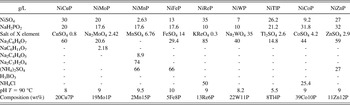
Before the electroless plating, the Cu substrate (1-mm thick) was polished to remove scratches, cleaned with acid, and activated with Pd solution, and the ternary NiXP UBM was made by adding salt of element X to the electroless nickel bath. Due to the difficulty of electroless plating two metallic elements simultaneously, only NiXP films with limited compositions were prepared. The compositions of the electroless plating baths and respective experimental conditions are presented in Table I. The electroless NiXP films were typically deposited to a thickness of 5-10 μm followed by immersion gold (IG) plating (0.05-μm thick). The latter step was used to suppress oxidation of the NiXP film and enhance the wetting performance with Sn-3.5 Ag solder. The crystallinity of the as-plated NiXP films without the IG process was analyzed by x-ray diffraction (XRD). Solder joints were made by reflowing Sn-3.5Ag solder paste over NiXP UBM under N2 gas. The peak temperature of reflowing was about 260 °C, and the reaction time above 220 °C was about 1 and 5 min. The joint microstructures were analyzed to nine points for each NiXP UBM using a scanning electron microscope (SEM) equipped with energy dispersive x-ray spectroscopy (EDX). A compositional analysis of the NiXP films was conducted by EDX having ±1% accuracy.
Compositions of electroless NiXP baths and plating conditions.

III. RESULTS AND DISCUSSION
A. Crystallinity of as-plated NiXP films
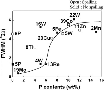
XRD peaks of as-plated NiXP films are presented in Fig. 1, and it can be seen that all the ternary electroless Ni films had a homogeneous phase without nucleating a second phase in the as-plated condition. The crystallinity of electroless NiXP films can be investigated by measuring the full width at the half maximum (FWHM) of Ni (111) peaks, and the results are presented in Fig. 2. In the figure, FWHM values of Ni-5P and Ni-9P films with nanocrystalline and amorphous structures, respectively, are presented as references. According to the FWHM data, the as-plated NiXP films can be classified into two groups: one with FWHM values close to that of nanocrystalline Ni5P film and another with values close to that of amorphous Ni9P film. It can be seen that the crystallinity of NiXP films depends on the P content of the film and deteriorates sharply around P content of 6–7 wt%. Since the amounts of alloying element and P vary, it is difficult to isolate the effect of each alloying element (X) at the same P level. However, it can be deduced from the FWHM data that 19Mo1P, 4W5P, and 13Re6P films have a nanocrystalline structure, whereas the other films have an amorphous structure in the as-plated condition. Spalling behaviors according to the FWHM are also presented in Fig. 2. Details of IMC spalling characteristics are explained below.
X-ray diffraction patterns of the as-plated NiXP films.

Measured full width at the half maximum (FWHM) of Ni (111) peaks of the as-plated NiXP films.

B. Solder joint microstructures
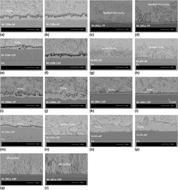
Backscattered SEM micrographs of as-reflowed NiXP/Sn-3.5Ag joints reflowed for 1 and 5 min at 260 °C are presented in Fig. 3. It can be seen that IMC growth kinetics and spalling behaviors depend on the UBM composition. In the case of nanocrystalline UBMs, 19Mo1P, 4W5P,Reference Jang and Yu21 and 13Re6P, Ni3Sn4 adhered well to the UBM and IMC spalling was not observed, and the same was true of some amorphous UBMs: 22W11P, 16W5P,Reference Jang and Yu21 5Fe8P, and 2Mn15P. However, 8Tl4P, 5W9P,Reference Jang and Yu21 20Cu7P, and 39Co10P UBMs are amorphous but showed IMC spalling ever after 1 min of reflow at 260 °C. In the case of 11Zn12P UBM, IMC spalling was observed after 5 min of reflow at 260 °C. Since amorphous Ni-P films without alloying elements show IMC spalling after reflow for P content larger than 7 wt%, the role of 20Cu, 5W, and 39Co remains unclear. It may be stated that the addition of 5Fe, 2Mn, and 22W to the Ni-P UBM effectively suppressed IMC spalling at the solder joints, although those UBMs remained amorphous. Note that the addition of 8 wt%Tl (4 wt%P) and 16 wt%W (5 wt%P), respectively, effectively stabilized the amorphous structure of UBM. However, 8Tl4P UBM was susceptible to IMC spalling after reflow with solder, suggesting a deleterious effect of Tl on the joint reliability. The occurrence of IMC spalling is a clear sign of the unsuitability of UBM because the spalled interface increases the vulnerability of solder joints to brittle fracture.Reference Jee, Yu and Ko2, Reference Sohn and Yu8
Solder joint microstructures of Sn-3.5Ag/NiXP after 1 (1st, 3rd column) and 5 min reflow (2nd, 4th column).

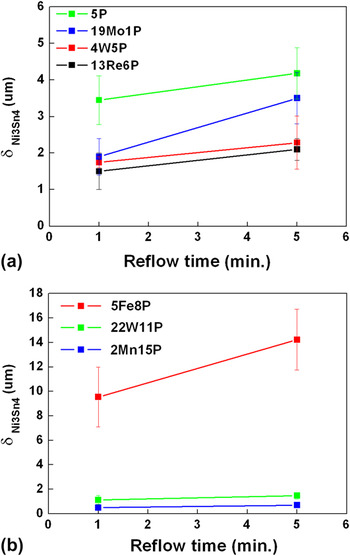
The effect of W addition on Ni-P UBM was recently reported by Jang and Yu,Reference Jang and Yu21 and it was shown that nanocrystalline Ni-5P film (as-plated) showed an amorphous structure with the addition of 16 wt%W and that IMC spalling was effectively prohibited when 22 wt%W was added to amorphous Ni-9P UBM. Between the Ni3Sn4 IMC and Ni-22W-9P UBM, an amorphous layer with composition of (Ni,W)3P was formed. It was thought that the new amorphous layer, which formed as a result of Ni depletion from the UBM, served as an intermetallic layer, which not only relieves the local stress but also improves the IMC adhesion to UBM. Among the alloying elements studied, only Cu and Ni atoms partitioned into Ni3Sn4 and CoSn2Reference Ratchev, Labie and Beyne23 IMCs, respectively. This is presumably due to the proximity of the atomic radius of Cu and Co to that of Ni, which would result in the smallest strain energy due to substitutional partitioning. SEM micrographs of Ni22W11P/Sn-3.5Ag joints after 500-h ageing at 150 °C are presented in Fig. 4. It can be seen that the spalling behavior of the IMC does not change during the ageing treatment unless IMC spalling occurred during the reflow process. In Fig. 5, the thickness of Ni3Sn4 IMCs after the solder reflow over various UBMs are presented. In the nanocrystalline UBMs, the addition of 13 wt%Re, 4 wt%W, and 19 wt%Mo suppressed IMC growth compared to Ni-5P without alloying UBM. Since the kinetics of Ni3Sn4 are controlled by the diffusion rate of Ni atoms from the Ni(P) UBM to the solder,Reference He, Chen and Qi24, Reference Yang, Lim, Kumar, Lee and Chen25 added transition elements to the UBM act as barriers to Ni diffusion. In contrast, Ni3Sn4 growth in amorphous UBM/solder joints was accelerated for 5Fe8P UBM but decelerated for 22W11P and 2Mn15P UBMs, as shown in Fig. 4(b) (Here, only solder joints that did not show spalling are plotted.). Thus, W and Mn atoms in amorphous UBMs are also thought to act as diffusion barriers to Ni atoms, similar to the cases of nanocrystalline UBM, but the role of Fe remains unclear at the moment. Cracks were found in the P-rich layer of the 2Mn15P/Sn-3.5Ag solder joint, which could be ascribed to tensile stress evolution in the UBM during the IMC formation.Reference Jee, Yu and Ko2, Reference Sohn, Yu, Kang, Shih and Lee7
Scanning electron microscopy micrograph of Sn-3.5Ag/Ni22W11P joint after 500 h ageing at 150 °C.

Ni3Sn4 thickness after reflow with Sn-3.5Ag solder for (a) crystalline and (b) amorphous NiXP under-bump metallurgies (UBMs) [specimens showing intermetallic compound (IMC) spalling was excluded].

C. IMC spalling map of NiXP/Sn-3.5Ag solder joints
The aim of this study is to find a new NiXP UBM that can be used with Pb-free solder, typically Sn-3.5Ag, which does not show IMC spalling or excessive IMC thickening. In Fig. 6, IMC spalling behaviors of various electroless NiXP UBMs after reflow are presented as functions of the alloying element (X) and P content. Solid symbols in the figure refer to NiXP UBMs of the given compositions without IMC spalling, whereas open symbols indicate the occurrence of IMC spalling. Thus, the demarcation line between solid and open symbols of a NiXP UBM refers to the boundary between spalling (typically high P and low X) and non-spalling (typically low P and high X) regions. In the absence of the alloying element, Ni-P UBM was nanocrystalline, which did not show IMC spalling after reflow for P content below 6 wt% but had an amorphous structure that showed IMC spalling at higher P content.
IMC spalling map of NiXP UBMs after a reflow (260 °C × 1 min).

In this process, we encountered two limitations. First, NiXP films with high (over 9 wt%) or low P (below 5 wt%) content were not adequate as UBM due to the formation of vertical cracks in the Ni3P layer during reflow and rapid growth of IMC.Reference Jee, Yu and Ko2, Reference Sohn, Yu, Kang, Shih and Lee7 Second, as the concentrations of the alloying element X in NiXP film exceeded ∼30 wt%, the deposition rate of the film rapidly dropped. Thus, NiXP films with 4–8 wt%P and 4–20 wt%X would be suitable as new UBMs. Within the limitations stated above and from the presented IMC spalling map, W and Re appear to be most promising elements for a new NiXP UBM. Here, Fe was not considered due to its role in accelerating IMC growth. The roles of other elements, particularly, Mo, Mn, and Zn, will be further clarified as NiXP UBMs with intermediate P concentration can be fabricated in the future.
IV. CONCLUSIONS
Ternary electroless Ni UBM was fabricated, and IMC spalling and growth of NiXP/Sn-3.5Ag solder joints were investigated. The crystallinity of the NiXP films was analyzed by measuring the FWHM of the Ni (111) peak. The crystallinity did not deviate significantly from that of binary Ni-P film, except that 8Tl4P and 16W5P films remained amorphous after the solder reflow. IMC growth in all crystalline (4W5P, 19Mo1P, 13Re6P) and amorphous (22W11P, 16W5P, 5Fe8P, 2Mn15P) films was smaller than that of Ni-P film with the exception of the 5Fe8P film. Among the ternary compositions analyzed in this study, IMC spalling was suppressed only in 22W11P, 5Fe8P, 11Zn12P, and 2Mn15P UBMs (after 1 min at 260 °C). From the IMC spalling map, within the limitation of 4–8 wt%P and 4–20 wt%X, W and Re are recommended as alloying elements X as they show potential to effectively replace the conventional Ni-P UBM by suppressing the IMC spalling and Ni3Sn4 growth simultaneously.
ACKNOWLEDGMENTS
This work was supported by a National Research Foundation of Korea grant funded by the South Korean Government Ministry of Education, Science and Technology (MEST) (Grant No. 2010-0000862).