I. INTRODUCTION
In modern communication systems, it is necessary to be able to handle multiple frequency bands. If two or three communication standards can be processed through one base station for a mobile phone, its construction price will be lowered with concomitant benefits for customers. Multiband is already common to cell phone designs for handling GPS, WiFi, and cellular bands. In order to support such multiband systems, a multiplexer is necessary if only one antenna covers all the designated spectra. Many researchers have investigated design methods for multiplexers, which can be categorized by star junction type and manifold junction type [Reference Macchiarella1–Reference Ismail, Smith, Panariello, Wang and Yu9]. In both star junction and manifold junction-type multiplexers, modification of filters and a complex optimization process are usually required. However, the capability of using commercial filters without any modification in a simple design method would be attractive for a system designer. Figure 1(a) shows a diplexer made of two isolation circuits satisfying such demand. Each isolation circuit consists of a conventional right-handed (RH) transmission line (TL) connected to a filter, and it has open-circuit input impedance at the center frequency of the other channel. Hence, the signal passes through one path while it is rejected by the other. Figure 1(b) shows the star-junction triplexer based on dual-band isolation circuits [Reference Lee and Itoh10]. Similarly to the diplexer shown in Fig. 1(a), each isolation circuit isolates itself from the input port at two operating frequencies of other circuits. In this concept, a composite right/left-handed (CRLH) TL having dual-band characteristic is essential [Reference Lin, Vincentis, Caloz and Itoh11, Reference Caloz and Itoh12], because the isolation circuits used for the triplexer should be designed to have the isolation characteristic at two frequencies. However, this method is more difficult for a contiguous or narrow guard band triplexer than the concept of a triplexer based on combining method of two filtering circuits (CMTC) shown in Fig. 1(c). The reason for this comes from the intrinsic characteristic of a band-pass filter (BPF) and a phase response of a CRLH TL. In the following section, detailed investigation will be discussed.
Diagrams and operation concepts of multiplexers. (a) Diplexer based on isolation circuits. (b) Star-junction triplexer based on isolation circuits. (c) The proposed triplexer based on CMTC.

In this paper, the contiguous channel triplexer based on CMTC is presented. The concept of the triplexer and the theory for an isolation circuit are explained. Also, the reason why the proposed method is attractive for a contiguous channel triplexer is investigated. The design process and the measured results of the proposed triplexer are also provided.
II. THEORY
A) Combining method of two filtering circuits
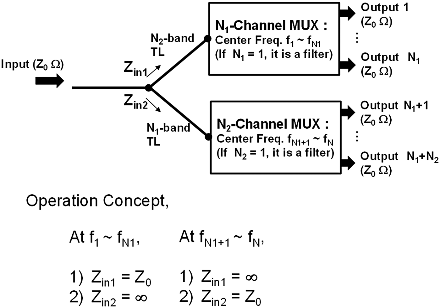
The general combining method of two filtering circuits (CMTC) represented in Fig. 2 uses two isolation circuits, as in the diplexer of Fig. 1(a) [Reference Lee, Sun and Itoh13, Reference Lee and Itoh14]. The difference between the diplexer and the CMTC is the use of a multi-band TL and a multiplexer, instead of a conventional RH TL and a filter. Since the CMTC uses a multi-band TL to combine multiplexers instead of an individual filter, it requires fewer isolation circuits compared to the star-junction multiplexer based on isolation circuits. The operation concept is also represented in Fig. 2. The isolation circuit, comprising an N 2-band TL and an N 1-channel multiplexer, has open-circuit impedance at the operating frequencies of the other isolation circuit (from fN1+1 to fN1+N2). On the other hand, the second isolation circuit, consisting of an N 1-band TL and an N 2-channel multiplexer, is isolated from the input port at frequencies from f 1 to f N1. Therefore, one circuit allows a signal path while the other circuit prevents a signal flow. For example, a signal having an f 1 frequency cannot enter the second isolation circuit, but the signal goes through the N 2-band TL of the first isolation circuit. Thereafter the signal is only detected at output port 1 because of the frequency selective characteristic of the N 1-channel multiplexer. The frequencies from f 1 to f N1+N2 do not need to be in ascending order as shown in Fig. 2.
Diagram and operation concept of combining method of two filtering circuits, where N 1 and N 2 are integer and N = N 1 + N 2.
The proposed triplexer (N 1 = 2 and N 2 = 1) is based on CMTC, and the diagram is shown in Fig. 1(c). The triplexer comprises two isolation circuits. One is composed with a CRLH TL and a filter. Another isolation circuit comprises a conventional TL connected with a diplexer. In this paper, the diplexer is also made by the use of CMTC presented in Fig. 1(a) with N 1 = 1 and N 2 = 1. In Fig. 1(c), the frequencies, in ascending order, are f 1, f 2, and f 3, and the center frequency of the filter used on CRLH isolation circuit should be f 2 for easier design of the CRLH TL, and this will be explained in the Section II-C.
B) Isolation circuit
Figure 3(a) shows the diagram of an isolation circuit. The main function of this is having infinite input impedance at the target frequency. If it is far from the target frequency, the isolation circuit will lose its isolation characteristic. In the isolation circuit design, it is essential to determine a proper phase response of a TL and to design the TL with solved phase response. Each triangle in Figs 3(b) and 3(c) shows an input impedance of a filter or a multiplexer at target frequency. In both cases, the real part of the impedance (α) is assumed zero for simplicity. A positive imaginary impedance and a negative imaginary impedance are shown in Figs 3(b) and 3(c), respectively. In order to have open-circuit impedance, a phase change is necessary for which a TL can be used. A clockwise rotation shows a RH phase response, ϕ 1, having a negative value. An LH phase response, ϕ 2, has a positive value and it is represented as a counter-clockwise rotation in the Smith chart. To solve phase responses ϕ 1 and ϕ 2, one can use the TL impedance equation [Reference Pozar15],
 $$Z_{in}=Z_0 \displaystyle{{Z_L+jZ_0 {\rm tan}\, \lpar {-} \phi _{1\comma 2} \rpar } \over {Z_0+jZ_L {\rm tan}\, \lpar {-} \phi _{1\comma 2} \rpar }}.$$
Since the input impedance of the circuit Z in should be infinite, the denominator of (1) is zero, and the required phase response, ϕ 1,2, is
 $$\phi _1=\left\{{\matrix{ { - \arctan \lpar Z_0 {\rm /}X{\rm \rpar \comma \; }}\hfill & {X\gt {\rm 0\comma \; }} \cr { - \pi - {\rm arctan}\, \lpar Z_0 {\rm /}X{\rm \rpar \comma \; }} & {X\lt {\rm 0\comma \; }} \cr } } \right.$$
 $$\phi _2=\left\{{\matrix{ {\pi - {\rm arctan}\, \lpar Z_0 {\rm /}X{\rm \rpar \comma \; }} & {X\gt {\rm 0\comma \; }} \cr { - {\rm arctan}\, \lpar Z_0 {\rm /}X{\rm \rpar \comma \; }}\hfill & {X\lt 0 .} \cr } } \right.$$
The simplified equation can be represented as
 $$\phi=n\pi - {\rm arctan}\, \lpar Z_0 {\rm /}X\rpar +\psi\comma \;$$
where n is an integer and Z 0 is the characteristic impedance of the TL. Here, ψ is the adjusting constant, which is generally used for obtaining reasonable circuit parameter of a TL [Reference Lee and Itoh16]. In this paper, ψ is not used for designing an isolation circuit.
(a) An isolation circuit diagram. (b) An example of the input impedance Z L shown on the Smith chart (case 1: X > 0 and α = 0). (c) An example of the input impedance Z L shown on the Smith chart (Case 2: X < 0 and α = 0).
For reference, a more rigorous equation considering the term α is also represented as
 $$\phi=n\pi - \displaystyle{{{\rm arg}\left\{{\lpar \alpha ^2+X^2 - Z_0^2 \rpar +j2Z_0 X} \right\}} \over 2}+\psi .$$
C) A simple contiguous channel implementation of the proposed triplexer
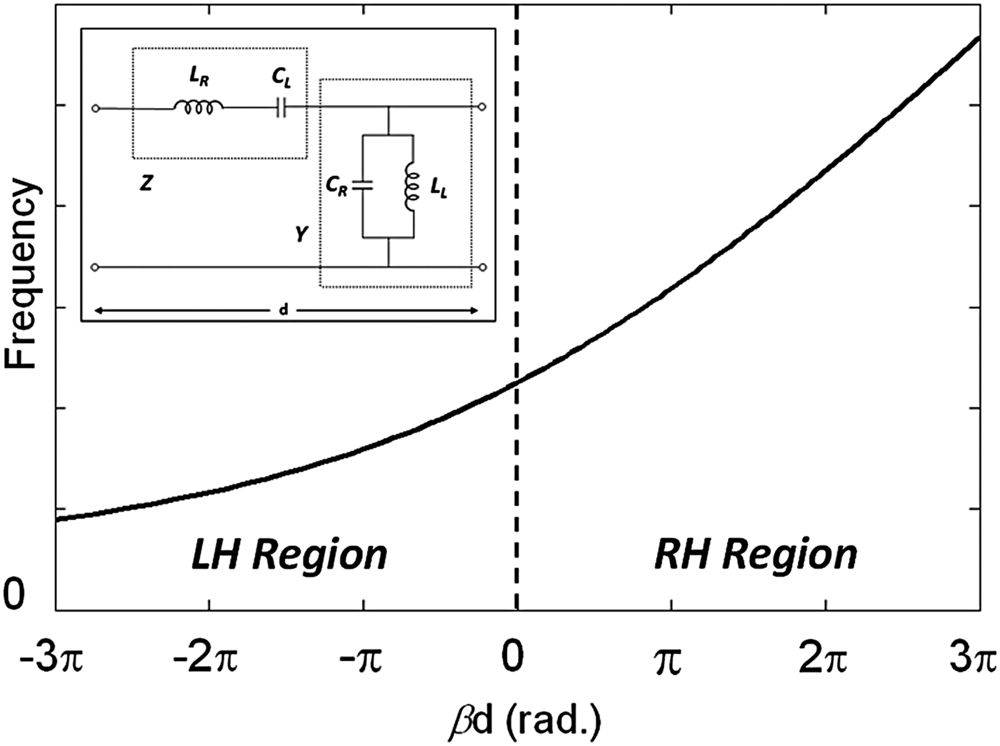
The proposed triplexer consists of an RH TL connected with a diplexer and a CRLH TL connected with a BPF. The appropriate phase response of the RH TL is determined by investigating the input impedance of the diplexer at the center frequency of the filter used in the CRLH isolation circuit. Adding proper phase delay of the RH TL, the isolation circuit consisting of the diplexer can have open circuit input impedance, which is not difficult to design with an RH TL. However, designing a CRLH TL for a contiguous channel triplexer is difficult or impractical in the circumstances that the filter connected with the CRLH TL has f 1 or f 3 center frequencies (f 1 < f 2 < f 3). The reason for this comes from the intrinsic characteristic of a BPF and a phase response of a CRLH TL. Figure 4 shows the locus of input impedance of a BPF shown in the Smith chart. An input impedance of a BPF having open rejection characteristics, in which the input impedance of the filter becomes closer to infinite impedance as the frequency moves away from the pass-band, is represented in Fig. 4(a), whereas Fig. 4(b) shows that of a BPF having short rejection characteristic (closer to zero impedance as far away from pass-band). In both cases, impedance follows locus with clockwise rotation as frequency is increasing because a general BPF always has a positive group delay. Detailed explanation of this is provided in the Appendix. Figure 5 shows the phase response of a CRLH TL, and both left-handed (LH) and RH phase responses exist.
Locus of input impedance of a BPF shown in the Smith chart. (a) Open rejection case. (b) Short rejection case.
Dispersion diagram of a CRLH TL (β: the propagation constant of a CRLH TL).
If a filter connected with a CRLH TL has f 2 center frequency, the input impedances of the filter at f 1 and f 3 are located on the Smith charts as shown in Fig. 6. With proper phase response of the CRLH TL, two impedance points can be moved to open-circuit impedance. Figure 6(a) shows the open rejection case, and the CRLH TL can be designed by selecting LH and RH phase responses (phase advance and phase delay) at f 1 and f 3, respectively. In the short rejection case shown in Fig. 6(b), same strategy used in the open rejection case could be difficult for design of the CRLH TL because required absolute phase responses at both f 1 and f 3 are large. Instead, only LH region of the CRLH TL can be used in this case. In the phase response of the CRLH TL shown in Fig. 6(b), both f 1 and f 3 belong to the LH region and the absolute phase response at f 1 has larger value than that at f 3. With this CRLH TL connected to the filter having the short rejection, open-circuit impedance can be realized at two target frequencies. This procedure cannot be used simply to a BPF (used on CRLH isolation circuit) having f 1 or f 3 center frequency. Figure 7 shows input impedance of the f 1 filter represented on the Smith chart. In the open rejection case shown in Fig. 7(a), the impedance point at f 3 requires smaller phase delay (RH phase response) than that at f 2 for having open-circuit impedance. However, a phase delay at higher frequency is always larger than that at lower frequency in a CRLH TL. Hence, the CRLH TL cannot satisfy the requirement of the f 1 filter connected with the CRLH TL having open-circuit impedance at both f 2 and f 3. With similar procedure of the open rejection case, it is difficult to design a CRLH TL for the short rejection f 1 filter. In Fig. 7(b), the impedance point at f 2 needs less phase advance (LH phase response) than that at f 3. However, a CRLH TL cannot support such phase response in the LH region. In the case of the filter having f 3 center frequency, it is still difficult to design a CRLH TL satisfying the required phase response for a dual-band isolation circuit. Figure 8(a) shows the case of the open rejection f 3 filter. For open-circuit impedance at f 1 and f 2, less phase advance at f 1 and more phase advance at f 2 are necessary; however, it is difficult to satisfy such condition using a CRLH TL. Figure 8(b) shows the short rejection case, and more phase delay at f 1 and less phase delay at f 2 are necessary. The phase response of a CRLH TL does not support this.
Design of CRLH TL connected with f 2 filter. (a) Open rejection case. (b) Short rejection case.
Design of CRLH TL connected with f 1 filter. (a) Open rejection case. (b) Short rejection case.
Design of CRLH TL connected with f 3 filter. (a) Open rejection case. (b) Short rejection case.
Considering Figs 6–8, it is found that using a filter having f 2 center frequency is easier for a CRLH isolation circuit of a contiguous channel triplexer. In addition, such case studies reveal that a star-junction triplexer, shown in Fig. 1(b), is not appropriate for a contiguous channel triplexer because CRLH TLs should be designed for f 1 and f 3 filters. However, the star-junction triplexer concept is valid in non-contiguous channel triplexers because interaction between channels is not strong and the adjusting constant ψ of (2c) can be used.
III. DESIGN PROCESS
In this section, the design process of the proposed triplexer is presented. Figure 9 shows the frequency response of the triplexer at output ports with ideal conditions. The combination of a diplexer shown in Fig. 10(a), whose center frequencies are 1 and 1.25 GHz, and a 1.125 GHz filter shown in Fig. 10(b) realizes the proposed triplexer. For compact size, hairpin-line filters are used for filtering circuits in the proposed triplexer [Reference Hong and Lancaster17]. The fractional bandwidths of the filters are about 10%, and it could be difficult to design the proposed triplexer with use of a filter having wide bandwidth because of band limitation of an isolation circuit. For reference, the diplexer is composed with two filters and it follows the simple design concept of Fig. 1(a). Figures 11(a) and 11(b) show the measured magnitude characteristics and input impedance of the diplexer, respectively. The measured results of the 1.125 GHz filter are shown in Figs 11(c) and 11(d). The frequency configuration of the triplexer is represented in Fig. 9, and its design procedure is as follows:
(1) Find an input impedance of a diplexer at the center frequency of a filter used on a CRLH isolation circuit, and check input impedances of the filter at operating frequencies of the diplexer used on the other isolation circuit. In the proposed triplexer, the input impedance of the diplexer at 1.125 GHz (marker 1 in Fig. 10(b)) and the input impedances of the 1.125 GHz filter at 1 and 1.25 GHz (markers 1 and 2 in Fig. 10(d)) are necessary for our design.
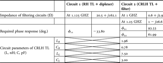
(2) Find the proper phase responses for each diplexer or filter using equation (2c) or (2d) in order to obtain open-circuit impedance at the target frequencies. In the proposed triplexer, the desired phase delay ϕ 11 for the diplexer is −33.80°, and the required phase shifts ϕ 21 and ϕ 22 for the filter are 93.33° and 61.99°, respectively.
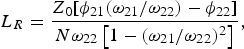
(3) Calculate circuit parameters of a CRLH TL and a length of a RH TL with solved phase responses in the procedure 2 above. In the proposed triplexer, the circuit parameters of the CRLH TL are solved by submitting (ϕ 21, ϕ 22) = {1.63 rad. (93.33°), 1.08 rad. (61.99°)} and (ω 21, ω 22) = (2 × π × 1 GHz, 2 × π × 1.125 GHz) pair and N = 2 to equations (3)–(6) [Reference Lee and Itoh10]. The circuit parameters of the CRLH TL are L R = 1.96 nH, C R = 0.78 pF, L L = 7.50 nH, and C L = 3.00 pF. For the diplexer, a conventional RH TL, having an electrical length of −33.80° at 1.125 GHz is necessary.
(3) $$L_R=\displaystyle{{Z_0 \lsqb \phi _{21} \lpar \omega _{21} /\omega _{22} \rpar - \phi _{22} \rsqb } \over {N\omega _{22} \left[{1 - \lpar \omega _{21} /\omega _{22} \rpar ^2 } \right]}}\comma \;$$(4)$$C_R=\displaystyle{{\phi _{21} \lpar \omega _{21} /\omega _{22} \rpar - \phi _{22} } \over {N\omega _{22} Z_0 \left[{1 - \lpar \omega _{21} /\omega _{22} \rpar ^2 } \right]}}\comma \;$$(5)$$L_L=\displaystyle{{NZ_0 \lsqb 1 - \lpar \omega _{21} /\omega _{22} \rpar ^2 \rsqb } \over {\omega _{21} \left[{\phi _{21} \lpar \omega _{21} /\omega _{22} \rpar - \phi _{22} } \right]}}\comma \;$$(6)$$C_L=\displaystyle{{N\lsqb 1 - \lpar \omega _{21} /\omega _{22} \rpar ^2 \rsqb } \over {\omega _{21} Z_0 \left[{\phi _{21} \lpar \omega _{21} /\omega _{22} \rpar - \phi _{22} } \right]}}.$$
(4) Combine a diplexer with an RH TL and connect a filter with a CRLH TL. In the proposed triplexer, the CRLH TL, designed in the procedure 3, and the 1.125 GHz filter make dual-band isolation circuit, and the combination of the diplexer and the conventional RH TL makes single-band isolation circuit.
(5) Connect two isolation circuits with common input port.



Ideal frequency response of the proposed triplexer on output ports.
The layout of filtering circuits used for the proposed triplexer. (a) Diplexer. (b) 1.125 GHz filter. (Parameters: l 11 = 5.9, l 12 = 28.55, l 13 = 14.25, l 14 = 37.45, l 15 = 14.45, l 21 = 6.8, l 22 = 31.7, l 23 = 16.2, l 24 = 41.6, l 25 = 17.4, l 31 = 8.1, l 32 = 35.1, l 33 = 20, l 34 = 46.9, l 35 = 19.8, w 0 = 2.3, w 1 = 1, w 2 = 1.8, and w 3 = 2.)
Performances of the diplexer and the filter used on the proposed triplexer. (a) Magnitude response of the diplexer. (b) Input impedance of the diplexer shown on the Smith chart. (c) Magnitude response of the filter. (d) Input impedance of the filter shown on the Smith chart.
IV. CONTIGUOUS TRIPLEXER
The proposed triplexer is composed of the single-band isolation circuit, a combination of the diplexer and the conventional TL, and the dual-band isolation circuit, which consists of a filter and a CRLH TL. In order to verify the design concept, the proposed triplexer is designed and fabricated. In Section III, the design process of the triplexer has been investigated, and the derived data are summarized in Table 1. In the fabricated triplexer picture shown in Fig. 12, the diplexer is located on the right side of the picture and the 1.125 GHz filter is on left side. An RT/Duroid 5870 substrate (ε r = 2.33, height = 0.787 mm) is used for the triplexer and hairpin-line BPFs are printed on the substrate for filtering circuits [Reference Hong and Lancaster17]. The lumped elements and the microstrip lines are used to form the CRLH TL. The LH part of the CRLH TL is realized by the lumped elements, and the microstrip lines are used for the RH part. For a single-band isolation circuit, the microstrip line which has 33.80° phase delay at 1.125 GHz is used.
Fabricated contiguous channel triplexer based on CMTC.
Summary of contiguous channel triplexer.
Ω = ohm, nH = nano henry, pF = pico farad.
Figure 13 shows the simulated and measured results of the contiguous triplexer. Figure 13(a) shows the insertion losses, which are less than 1.8 dB. The measured guard bandwidth is about 25 MHz. The return losses, shown in Fig. 13(b), are larger than 10 dB, whereas Fig. 13(c) shows that the isolation is >11.2 dB.
Simulated and measured results of the proposed triplexer. (a) Insertion loss. (b) Matching at port 1. (c) Isolation.
V. CONCLUSION
A contiguous channel triplexer based on CMTC has been presented. The measured results of the proposed triplexer show good agreement with the simulation results. The concept, theories, and design processes have been explained to help the reader design and fabricate this type of triplexer. It is usually difficult to design a contiguous or small guard band triplexer because of the strong interaction between the channels, and a designer is required to optimize filters or use a specific filter type. However, the proposed triplexer provides straightforward and simple design method. In addition, a system designer can choose any filter or diplexer without modification. Although a star-junction triplexer based on isolation circuits also has same advantages, it is difficult or nearly impossible to design CRLH TLs for a contiguous channel triplexer. Hence, the proposed triplexer is very attractive to a system designer.
Appendix
A second-order BPF has the transfer function of reflection coefficient of following mathematical form:
 $$H_{ref} \lpar s\rpar =\displaystyle{{A\lpar s^2+\omega _0^2 \rpar } \over {s^2+\lpar \omega _0 /Q\rpar s+\omega _0^2 }}=A\displaystyle{{\lpar s - z_1 \rpar \lpar s - z_2 \rpar } \over {\lpar s - p_1 \rpar \lpar s - p_2 \rpar }}\comma \;$$
where s = σ + jω, which is the complex frequency, ω 0 is the center frequency of the BPF, and Q stands for the quality factor. In addition, the constant A accounts for the rejection type at DC and infinite frequency (ω → ∞). If the stop band input impedance is infinite (open), A is equal to 1, whereas if the input impedance is zero (short) then A becomes −1. The above equation can be further expressed with the factored form in terms of poles (p i) and zeros (z i).
It is found useful that the frequency response of reflection coefficient S 11 can be visualized through the use of pole-zero plots. As an illustrative example shown in Fig. 14, four different frequencies from low to high (ω = 0, ω = ω 1, ω = ω 0, and ω = ω 2) are picked in order to examine the frequency response of the transfer function.
We can then construct frequency responses of the amplitude and phase from Fig. 14. By denoting the magnitude and phase of the pole vectors to be m i, φ i, and those of the zero vectors to be M i, θ i, where i = 1, 2, we can plot the amplitude response of the transfer function (M 1M 2/m 1m 2) and its phase response (θ 1+θ 2 − φ 1 − φ 2) as depicted in Fig. 15 [Reference Schaumann and Valkenburg18]. One can observe that the reflection zero occurs at ω 0, and at this frequency the phase experiences an abrupt change from −90° to +90°. Overall, the phase is decreasing with respect to the frequency, which implies the transfer function of reflection coefficient has a positive group delay. As a result, the overall phase of the transfer function will be decreasing. Furthermore, if we plot the response on Smith charts, such characteristics will result in a clockwise rotation of S 11 with frequency increasing. Figure 4 plots the corresponding responses of S 11 or input impedance of the filter when the rejection is open (A = 1) and short (A = −1), and they both rotate clockwise on the Smith charts.
Pole-zero plots of the transfer function of reflection coefficient at (a) ω = 0, (b) ω = ω 1, (c) ω = ω 0, and (d) ω = ω 2.
(a) Amplitude and (b) phase response of the reflection coefficient of a BPF.
Although the case discussed here is for a second order BPF, any high-order BPFs' transfer functions can be decomposed to a multiplication of second-order BPFs. Therefore, the same analysis can be used and will still result in the same conclusion for the sense of phase rotation.
Hanseung Lee received the B.S. degree from the Korea University, Seoul, Republic of Korea, in 2006, and the M.S. degree from the Seoul National University, in 2008, both in Electrical Engineering and he is currently working toward the Ph.D. degree in Electrical Engineering from the University of California at Los Angeles (UCLA). Since September 2010, he has been a Graduate Student Researcher at the Microwave Electronics Laboratory, UCLA. His research interests include design of a passive circuit and an antenna for RF/microwave, and applications of metamaterials. Mr. Lee is the recipient of Asia-Pacific Microwave Conference (APMC) 2011 Prize.
Chung-Tse Michael Wu received his B.S. degree from National Taiwan University (NTU) and M.S. degree from the University of California at Los Angeles (UCLA) in 2006 and 2009, respectively, both in Electrical Engineering. He is currently working toward the Ph.D. degree in the Department of Electrical Engineering, University of California at Los Angeles (UCLA). Since September 2008, he has been a Graduate Student Researcher at the Microwave Electronics Laboratory in UCLA. In 2009, He worked as a summer intern in Bell Laboratories, Alcatel-Lucent, Murray Hill, NJ. He is the recipient of Asia-Pacific Microwave Conference (APMC) 2011 student prize. His research interests include active antennas, microwave systems, and metamaterials.
Tatsuo Itoh received the Ph.D. degree in Electrical Engineering from the University of Illinois, Urbana in 1969. After working for University of Illinois, SRI and University of Kentucky, he joined the faculty at the University of Texas at Austin in 1978, where he became a Professor of Electrical Engineering in 1981. In January 1991, he joined the University of California, Los Angeles as Professor of Electrical Engineering and holder of the TRW Endowed Chair in Microwave and Millimeter Wave Electronics (currently Northrop Grumman Endowed Chair). He received a number of awards including IEEE Third Millennium Medal in 2000, and IEEE MTT Distinguished Educator Award in 2000. He was elected to a member of National Academy of Engineering in 2003. In 2011, he received Microwave Career Award from IEEE MTT Society. He has 420 journal publications, 820 refereed conference presentations and has written 48 books/book chapters in the area of microwaves, millimeter-waves, antennas, and numerical electromagnetics. He generated 75 Ph.D. students.