I. INTRODUCTION
Gallium oxide (Ga2O3) has attracted great interest because of its potential for the next-generation of power electronics. The advantage Ga2O3 has over other materials, such as GaN and SiC, is that Ga2O3 has a larger band gap of 4.8–4.9 eV, a higher estimated breakdown field of 8 MV/cm, Reference Higashiwaki, Sasaki, Kuramata, Masui and Yamakoshi1 and a lower cost to produce the native substrates. Reference Villora, Shimamura, Yoshikawa, Aoki and Ichinose2,Reference Aida, Nishiguchi, Takeda, Aota, Sunakawa and Yaguchi3 The electron mobility of ∼100 cm2/V s in Ga2O3 at room temperature has been reported Reference Oishi, Koga, Harada and Kasu4,Reference Irmscher, Galazka, Pietsch, Uecker and Fornari5 and could be higher with further improved material quality. It has been estimated that the Baliga’s figure of merit of β-Ga2O3 is more than four times larger than those of 4H–SiC and GaN. Reference Higashiwaki, Sasaki, Kuramata, Masui and Yamakoshi1 Extensive studies have been performed on material growth Reference Sasaki, Kuramata, Masui, Villora, Shimamura and Yamakoshi6,Reference Sasaki, Higashiwaki, Kuramata, Masui and Yamakoshi7 as well as physical properties, like the thermal conductivity and the dielectric constant. Reference Guo, Verma, Wu, Sun, Hickman, Masui, Kuramata, Higashiwaki, Jena and Luo8,Reference Passlack, Schubert, Hobson, Hong, Moriya, Chu, Konstadinidis, Mannaerts, Schnoes and Zydzik9 Both lateral transistors Reference Higashiwaki, Sasaki, Kuramata, Masui and Yamakoshi1,Reference Higashiwaki, Sasaki, Kamimura, Wong, Krishnamurthy, Kuramata, Masui and Yamakoshi10,Reference Wong, Sasaki, Kuramata, Yamakoshi and Higashiwaki11 and vertical Schottky diodes Reference Oishi, Koga, Harada and Kasu4,Reference Sasaki, Kuramata, Masui, Villora, Shimamura and Yamakoshi6 have been fabricated on Ga2O3 with the hope of demonstrating a better figure of merit (FOM) than GaN and SiC. However, the development of vertical Ga2O3 transistors is currently limited by the lack of stable p-type doping. The valence band offset between GaN and β-Ga2O3 was reported to be 1.4 eV. Reference Wei, Qin, Fan, Li, Shi, Zhu and Zhang12 This indicates the conduction band offset is less than 0.1 eV, making it very attractive to integrate GaN-based devices with Ga2O3 substrates or even Ga2O3 devices because of the availability of both n-type and p-type doping capability in GaN, and the possible vertical conduction between GaN and Ga2O3. But this approach requires high-quality hetero-epitaxy as well as in-depth understanding of the growth mechanisms for GaN and Ga2O3 materials. This paper will make preliminary exploration in this area.
II. EXPERIMENT
Epitaxy of c-plane GaN has been achieved on β-Ga2O3 substrates with different orientations including (−2 0 1), (1 0 0), (1 0 1), (3 1 0), (3 −1 0) by MBE, HVPE, and MOCVD methods. Reference Sasaki, Kuramata and Yamakoshi14–Reference Rogan and Muhammed23 c-Plane GaN LED devices have also been demonstrated on (1 0 0) β-Ga2O3 substrates. Reference Xie, Zhang, Xia, Xiu, Han, Liu, Zhao, Jiang, Shi and Zheng21,Reference Villora, Arjoca, Shimamura, Inomata and Aoki22 Since Ga2O3 can be manufactured by melt growth like the film fed growth, the floating zone and the Czochralski methods adopted by silicon industry Reference Aida, Nishiguchi, Takeda, Aota, Sunakawa and Yaguchi3,Reference Zhang, Li, Xia, Pei, Deng, Yang, Xu, Shi, Wu and Wu24,Reference Galazka, Uecker, Irmscher, Albrecht, Klimm, Pietsch, Brutzam, Bertram, Ganschow and Fornari25 it is possible to achieve large-scale substrates at low cost. Conductive, transparent, and wide-band-gap substrates are particularly desired by the nitride optoelectronics market. Ga2O3 could offer the advantage of light extraction through substrates as well as the capability of handling high current density through the vertical structure and bulk substrate.
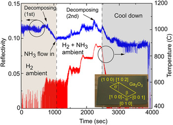
β-Ga2O3 substrates with several orientations are commercially available in the market. Substantial progress has been made in Ga2O3 devices on (−2 0 1) substrates, Reference Oishi, Koga, Harada and Kasu4,Reference Oshi, Harada, Koga and Kasu13 however it is known that Ga2O3 growth rate on this plane is low Reference Sasaki, Kuramata, Masui, Villora, Shimamura and Yamakoshi6 and stacking faults are easy to generate in the plane. Reference Sasaki, Kuramata and Yamakoshi14 (0 1 0)-Ga2O3 is another option and has also been used for oxide device fabrication. Previous study showed that the thermal conductivity is anisotropic in β-Ga2O3, and is the highest along the [0 1 0] direction. Reference Guo, Verma, Wu, Sun, Hickman, Masui, Kuramata, Higashiwaki, Jena and Luo8 The growth rate of Ga2O3 epitaxy in the (0 1 0) plane was also reported to be higher than that achieved from other planes. Reference Sasaki, Kuramata, Masui, Villora, Shimamura and Yamakoshi6 Therefore considering possible integration of nitride and Ga2O3 based devices in the future, the substrates used in this paper are all (0 1 0)-plane β-Ga2O3 with the size of 10 × 15 mm2, purchased from Novel Crystal Technology, Inc. (Saitama, Japan). The inset of Fig. 1 shows the substrate image with the miller indices and the model of unit cell labeled. According to β-Ga2O3’s lattice structure Reference Bermudez26 and previous TEM study, Reference Nakagomi and Kokubun27 the angle β between the a-axis ([1 0 0]) and the c-axis ([0 0 1]) is 103.7°, and the angle θ between the [1 0 2] direction and the (1 0 0) plane is 53.8°.
Plot the surface reflectivity and the wafer temperature as a function of time measured by in situ monitoring system. The inset shows the sample image with the substrate orientation labeled.

A closed coupled showerhead MOCVD reactor was used for nitride film epitaxy on Ga2O3. We customized a wafer holder for the Ga2O3 substrates so that we were able to measure real-time wafer temperature, wafer curvature, and surface reflectivity during growth by a commercial in situ monitoring system. The thermal stability of β-Ga2O3 under both H2 and N2 ambient has been carefully studied. It was reported that the Ga2O3 film started decomposing at only 350 °C under H2. Reference Togashi, Nomura, Eguchi, Fukizawa, Goto, Thieu, Murakami, Kumagai, Kuramata, Yamakoshi, Monemar and Koukitu28 In our case, MOCVD epitaxy of GaN was generally performed in the range of 600–1050 °C with the ammonia cracking temperature at ∼520 °C. Reference Ghrib, Boubaker and Bouhafs29 The wafer temperature was measured by a pyrometer, which is capable of measuring temperature above 600 °C. Thus we studied Ga2O3 thermal stability at 600 °C or above by heating up the substrate to 600 °C at the rate of 1 °C/s under H2 ambient with a 20 slm H2 flow and the reactor pressure of 100 torr. As Fig. 1 shows, the circled dip in the reflectivity before the temperature reached 500 °C could be a signal of Ga2O3’s early decomposition, consistent with previous study. Reference Togashi, Nomura, Eguchi, Fukizawa, Goto, Thieu, Murakami, Kumagai, Kuramata, Yamakoshi, Monemar and Koukitu28 When the temperature reached ∼600 °C, the reflectivity started to degrade fast, indicating the surface became rough due to the Ga2O3 decomposition. After NH3 gas was introduced into the chamber while keeping H2 flow unchanged as the carrier gas, the substrate surface was nitridized and hence the degradation stopped. Then the temperature was further increased. After every increase of 100 °C, the temperature was held for 5 min for reflectivity measurement. With the protection of NH3, the Ga2O3 surface stayed stable up to ∼880 °C. At temperatures above 880 °C the surface started to decompose again. Since the heater is under PID control, which was optimized for the range of GaN growth temperature (∼1000 °C), several temperature overshoots can be seen in Fig. 1. Since reflectivity is particularly coupled to temperature, reflectivity overshoots can be seen as well. It usually took 1–1.5 min for the wafer temperature to become stable. Similar experiment was also performed for Ga2O3 substrates under N2 ambient. The Ga2O3 surface stayed stable up to ∼930 °C no matter if ammonia existed in the chamber. At or above 960 °C, the surface smoothness decayed slowly with only N2 flowing, and very fast with an ammonia flow of 3 slm introduced. This shows at high temperature, the hydrogen released by cracked ammonia etches Ga2O3 aggressively.
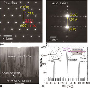
As reported in the TEM results by Tsai et al., Reference Tsai, Horng, Wuu, Ou, Hung and Hsueh30 the [1 1 −2 0 direction in the c-plane GaN grown on (−2 0 1) Ga2O3 substrates aligned with its [0 1 0] direction. Thus if GaN could be grown on (0 1 0) Ga2O3, it is possibly a non-polar film. As for a-plane non-polar GaN growth along its [1 1 −2 0] direction on r-plane sapphire substrates, it has been reported that it prefers low V/III molar ratio, with the help of an AlN nucleation layer (NL) grown at a high temperature and a GaN buffer layer grown at a low temperature. Reference Sun, Kong, Yerino, Ko, Leung, Cho and Han31 Considering the poor thermal stability of (0 1 0)-plane β-Ga2O3 substrates, we adopted a two-step growth. The first step was an ∼18 nm AlGaN NL grown at ∼600 °C under pressure of 100 torr. The second step was a 1.36 μm high-temperature GaN epitaxial layer grown at ∼1000 °C under pressure of 50 torr. The aluminum composition in the AlGaN was around 20%. A high V/III molar ratio of 2223 was used for the AlGaN NL while a low V/III molar ratio of 216 was used for the top GaN layer. The GaN growth rate was ∼0.75 nm/s. Transmission electron microscopy (TEM) was used to determine the GaN film orientation, as well as the defects in the epitaxial layers. The focused ion beam (FIB) was performed perpendicularly to the [1 0 2] direction of the Ga2O3 substrate, which was parallel to the 15 mm edge. GaN film orientation was determined by the selected area diffraction patterns (SADPs) from both GaN and Ga2O3 substrate, shown in Figs. 2(a) and 2(b) respectively. The g vector in yellow in Fig. 2(a) corresponded to a d-spacing of 1.55 Å, matching that from the {1 1−2 0} planes. The g vector in red pointed to the (1 −1 0 0) plane with the d-spacing of 2.76 Å. These patterns confirmed that the GaN was grown along the [1 1 −2 0] direction. The viewing direction (zone axis) was along [0 0 0 1]—c-axis. The SADP image of the Ga2O3 substrate along the same viewing direction is shown in Fig. 2(b). This direction is not on zone axis of Ga2O3. Therefore some strongly excited spots were missing. The g vector in yellow represents a distance of 1.51 Å, which is half of the lattice constant b of β-Ga2O3 as well as the d-spacing of (0 2 0) planes of Ga2O3, as the yellow arrow pointes to. This is consistent with the known (010) orientation.
TEM images of the selected area diffraction patterns for (a) the GaN film and (b) the Ga2O3 substrate, and (c) the bright field image showing threading dislocation in GaN. (d) Chi-scan by X-ray diffraction was used to identify the symmetry of the GaN film. The inset of (d) shows the (0001) GaN basal plane and the Chi scan set-up.

Bright field image is shown in Fig. 2(c) with the AlGaN nucleation layer shown by the arrow. The threading dislocation density was accordingly estimated to be ∼9 × 1010 cm−2 in the surface (1 1 −2 0) plane and will be further reduced with optimized growth conditions. X-Ray diffraction was also used to identify the symmetry of the non-polar GaN film. As the insets of Fig. 2(d) shows, the X-ray should always see the same {1 1−2 0} planes when the sample rotates along the c-axis of GaN by ± 60°. Thus we performed the Chi-scan by optimizing the (1 1−2 0)-plane signal with the sample vertically mounted, and rotate the sample along the c-axis. In the allowed scanning range, we got three peaks with the separation of 60°. All the above results show that we have single-crystal GaN film epitaxially grown on the (0 1 0) Ga2O3 substrate. To our knowledge, it is the first time that non-polar GaN epitaxy on β-Ga2O3 substrates has been reported. It may provide broad application in high-efficiency LEDs since the quantum Stark effect caused by polarization is removed and the electron–hole recombination efficiency can be largely improved. Reference Detchprohm, Zhu, Li, Xia, Wetzel, Preble, Liu, Paskova and Hanser32
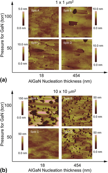
The effects of the AlGaN NL thickness and the GaN growth pressure were studied. As described in Table I, four growths were performed. The AlGaN NL thickness was ∼18 nm in splits A and C, and ∼454 nm in splits B and D. The growth rate for the NL was ∼0.45 nm/s. The top layer of GaN was grown at a pressure of 50 torr in split C and D, and at a pressure of 100 torr in split A and B. The other growth conditions are the same as that used for the sample shown in Fig. 2. The surface morphology of GaN film was studied by atomic force microscopy (AFM), and plotted in Fig. 3 as a function of the GaN growth pressure and the NL thickness. To better show the details on surface, the height scale was adjusted to 5 nm for split A and 10 nm for the other three splits in Fig. 3(a), and 150 nm for split A with 50 nm for the rest in Fig. 3(b). Growing GaN under pressure of 100 torr caused incomplete coalescence in the film. The surface roughness of split A was the largest among the four splits. Using 454-nm-thick AlGaN NL helped improve surface smoothness but still resulted in a lot of pits no matter if the GaN growth pressure was 50 torr or 100 torr. This indicates the AlGaN NL is very rough and it could take more time for GaN film to coalesce. The best surface morphology was achieved in split C by using an 18 nm AlGaN NL, and 50 torr pressure for the top GaN growth. No obvious pits can be seen from 10 × 10 μm2 scan, as shown in Fig. 3(b). The root mean square roughness (RMS) for split C is 0.98 nm for 1 × 1 μm2 scan and 3.15 nm for 10 × 10 μm2 scan respectively. These values are comparable to those achieved from GaN homoepitaxy on a-plane GaN bulk substrates. Reference Detchprohm, Zhu, Li, Xia, Wetzel, Preble, Liu, Paskova and Hanser32 For completeness, the RMS values from other splits are listed in Table I.
Characterization of surface morphology by AFM and the FWHM of rocking curve by X-ray measurements.

AFM scan of (a) 1 × 1 μm2 and (b) 10 × 10 μm2 GaN surface as a function of the AlGaN NL thickness and the pressure used for GaN growth.

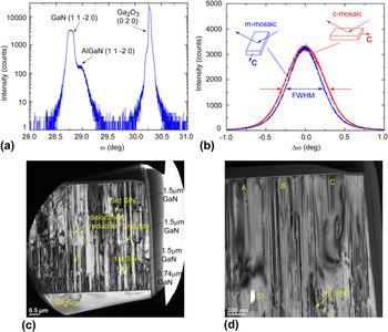
Figure 4(a) shows the result of ω–2θ scan by X-ray diffraction performed in the GaN (1 1−2 0) plane of split D, with the peaks labeled for AlGaN and (0 2 0) Ga2O3. The d-spacing represented by the GaN peak is 1.594 Å, indicating that the lattice constant a is 3.188 Å, consistent with the values reported in literature. Reference Monemar, Lagerstedt and Gislason33 It has been reported that the crystal tilt mosaic of nonpolar GaN on a-plane SiC substrates was orientation dependent, as determined by X-ray rocking curve measurements. Reference Craven, Wu, Chakraborty, Imer, Mishra, DenBaars and Speck34 Similar measurements were performed for all four splits, where the full width at half maximum (FWHM) values were extracted from measurements along the GaN c-axis (c-mosaic) and m-axis (m-mosaic). This serves as an indicator of the microstructure’s mosaic tilt, in the directions of [0 0 0 1] and [−1 1 0 0] separately. As listed in Table I, split A, B, and C had the mosaic ratio close to 1, which is consistent with a previous report about a-plane GaN with the film thickness close to 1 μm. Reference Craven, Wu, Chakraborty, Imer, Mishra, DenBaars and Speck34 Split D had the c-mosaic much larger than the m-mosaic, as shown in Fig. 4(b) where the rocking curves are normalized for comparison. This shows that the GaN grown at low pressure on the thick AlGaN NL had more microstructure tilt along the c-axis, indicating a preference for the lateral growth in the [−1 1 0 0] direction over that in [0 0 0 1]. Our study also showed the GaN growth was more stable with a low V/III ratio. The GaN surface roughness increased with the V/III ratio, especially when the GaN film thickness was above 2 μm. Therefore we focused in dislocation mitigation in the GaN films grown with low V/III ratios in the following study using SiN interlayers.
X-ray measurement for (a) Ω–2θ scan for GaN (1 1−2 0) plane, and (b) the normalized rocking curve for GaN (1 1–2 0) measured along the GaN c-axis (red) and the GaN m-axis (blue). The inset of (b) shows the schematic plot of the measurement set-up. TEM images show (c) an overview of the structure of GaN grown on Ga2O3 substrates with three SiN interlayers and (d) a zoomed-in view of the top GaN layer.

In situ SiN interlayers were used to reduce threading dislocation density in c-plane GaN grown by MOCVD, Reference Naoi, Tada, Li, Jiang and Sakai35 and was found to be effective in our a-plane GaN growth too. Figures 4(c) and 4(d) show the cross section TEM images of bulk GaN layer grown on a Ga2O3 substrate with three in situ SiN interlayers inserted in the middle. The g vector was along the [−1 2 −1 0] direction. In Fig. 4(c), the structure contained the same 18 nm AlGaN NL and 740 nm GaN layer before the first SiN interlayer was grown, followed by three GaN layers ∼1.5 μm thick separated by SiN interlayers. The all the GaN and the SiN layers were grown at ∼1000 °C under the pressure of 75 torr. A disilane flow of 1 sccm was used for the 20 s SiN growth. In Fig. 4(c) the first two SiN interlayers greatly reduced the threading dislocation density. The third SiN interlayer had much less impact compared to the other two. The sample surface was zoomed in, as shown in Fig. 4(d). The dislocation density is not uniform across the surface. Three areas marked by “A”, “B” and “C” had dislocation density of ∼1.5 × 1010 cm−2, ∼6.3 × 1010 cm−2, and ∼3.9 × 109 cm−2 separately. By average the threading dislocation density was ∼3 × 1010 cm−2 at the surface, compared to ∼2.3 × 1011 cm−2 in the bottom GaN layer grown on the AlGaN NL. The bright spot, labeled as “D”, close to the third SiN interlayer was a void where the GaN film did not coalesce. Based on previous study in Fig. 3, it is expected that the combination of SiN interlayers and growth pressure of 50 torr will further improve the film coalescence and result in less dislocations. The nonuniform dislocation distribution should be related with the SiN coverage on GaN, which is determined by the growth time and requires more optimization. Basal-plane stacking faults (BSFs) with the line density as high as 4 × 105 cm−1 were also observed from TEM images. The SiN interlayers did not reduce the BSFs as effectively as it did on dislocations.
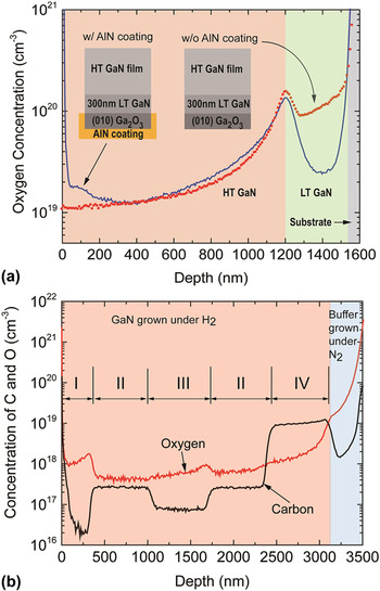
The major contamination source in the nonpolar GaN film was oxygen, as identified by the secondary ion mass spectrometry (SIMS) method. To investigate if the oxygen doping in the GaN film was due to oxygen diffusion from the nitride/oxide growth interface, we coated one gallium oxide substrate’s backside with 5 μm sputtered AlN. The sample was rotated during sputtering to ensure the sidewall coverage as well. Another sample does not have any AlN coating applied. As the inset of Fig. 5(a) shows, the same GaN structures were grown on both substrates under H2 ambient, including a 300 nm GaN buffer grown at 650 °C and a 1 μm GaN layer grown at 1020 °C. The SIMS results shown in red dots in Fig. 5(a) indicates that in the sample without AlN coating, the oxygen concentration in all GaN layers was above 1019 cm−3. The 300 nm low-temperature (LT) GaN buffer did not suppress oxygen incorporation in GaN. The blue lines in Fig. 5(a) shows reduced oxygen concentration in the LT GaN. But as the growth temperature ramped up, the oxygen concentration increased in the GaN film grown at 1020 °C. The concentration dip in the LT GaN layer of the coated sample indicates the oxygen diffused from the nitride/oxide growth interface was not the only source of oxygen incorporation and most oxygen incorporation was from the substrate decomposition under H2 ambient. AlN coating could reduce the oxide decomposition at low temperature but could not effectively protect the substrate at high temperatures.
SIMS results for (a) oxygen in GaN grown on Ga2O3 substrates with and without AlN backside coating, and (b) carbon and oxygen in HT GaN grown on top of LT GaN buffer grown under N2 ambient. Four different growth conditions (I, II, III, and IV) were performed for HT GaN.

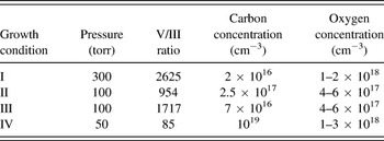
Since our study of oxide stability indicates that the gallium oxide is sensitive to hydrogen and more stable under N2 ambient, we performed the 300 nm-thick LT GaN buffer grown at ∼650 °C under N2 ambient. Then the carrier gas was switched to H2 to grow the following GaN layers at 1020 °C with four different conditions described in Table II and labeled in Fig. 5(b). The growth pressure varied from 50 torr to 300 torr with varied V/III ratios in the range of 85–2625. The growth rate of GaN was about 0.2 nm/s under Condition I, and 0.7–0.8 nm/s under Conditions II, III, and IV. Both the concentration curves of oxygen and carbon by SIMS are plotted in Fig. 5(b). In most GaN layers, the oxygen concentration is below 1018 cm−3, more than one order of magnitude reduction compared to that in Fig. 5(a). The increase of oxygen in the layer grown at 300 torr was due to reduced growth rate at high pressure and high V/III ratio. By adjusting growth conditions, the carbon concentration in GaN varies in the range of 2 × 10¹⁶–1019 cm−3, in the same manner of c-plane GaN growths. These results indicates initializing GaN growth under N2 ambient helps reduce substrates decomposition and lower the oxygen level in GaN. To further reduce oxygen contamination, more optimization of the growth scheme is required but is not in the scope of this paper.
Growth conditions of HT GaN with the concentration of carbon and oxygen by SIMS.

III. CONCLUSION
In conclusion, we have studied the thermal stability of (0 1 0) Ga2O3 substrates and demonstrated a-plane non-polar GaN growth on β-Ga2O3 by MOCVD using a low-temperature AlGaN NL. The effects of AlGaN NL thickness and the GaN growth pressure have been studied. To achieve the best surface morphology, low V/III molar ratio and low pressure were desired. In situ SiN interlayers provide an approach to effectively reduce the dislocation density by over 60%. The oxygen incorporation in GaN was found to be caused by the substrate decomposition under H2 ambient. By applying LT GaN buffer grown under N2 ambient, the oxygen concentration was lowered more than 10 times. Further improvement in a-plane GaN quality on Ga2O3 will provide an approach to integrate nitride-based devices with Ga2O3-based epitaxial structures, which is promising for both optoelectronics and electronic applications.
ACKNOWLEDGMENT
The authors acknowledge the helpful discussion with Akito Kuramata and Kohei Sasaki from Novel Crystal Technology (Japan), Professor Takayoshi Oshima from Saga University (Japan), Professor Tom Kosel from University of Notre Dame, Dr. Lancy Tsung from EAG, and the on-going support of Bill McGovern, Hussein Anton, Michael Brown and David Chow.