I. INTRODUCTION
Recently, organic and inorganic perovskite structures have emerged as efficient absorbers for solar cells. Although their power conversion efficiency (PCE) was around 4% in 2008, Reference Kojima, Teshima, Shirai and Miyasaka1 values exceeding 20% have now been achieved. Reference Green, Emery, Hishikawa, Warta, Dunlop, Levi and Ho-Baillie2 The theoretical limit is estimated to be around 30%, which is superior to silicon solar cells. Reference Sha, Ren, Chen and Choy3 Furthermore, perovskite materials are expected to be suitable as absorbers for tandem solar cells. Reference Service4 Accordingly, perovskite solar cells have attracted the attention of many researchers. In particular, the ability to form perovskite structures by solution processing offers advantages for low-cost manufacturing. In the past, many methods have been proposed for obtaining high PCEs including the one-step method, two-step method, and antisolvent method, Reference Ahn, Son, Jang, Kang, Choi and Park5–Reference Jeon, Noh, Kim, Yang, Ryu and Seok7 and in 2014, the gas blowing method was reported as a suitable method. Reference Huang, Dkhissi, Huang, Xiao, Benesperi, Rubanov, Zhu, Lin, Jiang, Zhou, Gray-Weale, Etheridge, McNeill, Caruso, Bach, Spiccia and Cheng8 The method was applied to the formation of perovskite on TiO x because the focus was on the mesoporous structure of solar cells, and it was reported that the method increased the PCE of only this type of perovskite solar cell. There are three main types of perovskite solar cell structures (mesoporous structure, planar structure, and inverted structure). Reference Meng, You, Guo and Yang9 The mesoporous structure is the most well-known structure because perovskite solar cells originated from dye-sensitized solar cells. In this structure, a PCE of 20.2% has been reported for an active area of 1 cm2. Reference Li, Bi, Yi, Décoppet, Luo, Zakeeruddin, Hagfeldt and Grätzel10 However, this structure basically requires high process temperatures to form the electron transport layer (ETL) and the mesoporous TiO x (mp-TiO x ). Early works reported the planar structure and inverted structure as new types of structures that did not use mp-TiO x , and this allowed perovskite solar cells to be made using low process temperatures. For the planar structure, Miyasaka’s group achieved a PCE of 14% by replacing the ETL with a material that can be created using low process temperatures, Reference Song, Zheng, Bian, Wang, Tian, Sanehirac and Miyasakac11 and they demonstrated flexible perovskite solar cells using this structure. The inverted planar structure can be made at low temperatures because the structure can be made using organic materials, with a PCE of 20.3% achieved despite a low process temperature of only 100 °C. Reference Wang, Dong, Li, Gruverman and Huang12 The inverted planar structure is expected to be applicable to flexible solar cells in the future.
We have previously investigated the inverted structure fabricated using a low temperature process and used a gas blowing method to form the perovskite layer for the inverted structure. The gas blowing method is similar to the one-step method (see Fig. S1 in the Supplementary Material) but differs in that the surface of the precursor solution is blown during the spin coating. We examined the use of this effect to form MAPbI3 on organic scaffolds and reported cases for which the method was suitable. Reference Gotanda, Mori, Matsui and Oooka13 The method can form a flat perovskite layer with low defect density and can provide a highly reproducible PCE. The observed high X-ray diffraction of the (310) plane suggested a crystal growth process different from that in the one-step method. Xia et al. reported a combination technique of using an antisolvent method to fabricate inverted cells that exhibited good performance. Reference Xia, Wu, Dong, Xi, Wu, Lei, Xi, Yuan, Jiao, Xiao, Gongb and Hou14 However, antisolvent methods require a quick coating technique above the surface of the perovskite precursor solution by an antisolvent. Because there is no option available for large-scale coating, quick coating poses a serious problem for realizing industrial production. In this study, we used only the gas blowing method in the formation of MAPb(I(1−X)Br X )3 without using an antisolvent technique.
Perovskite materials have an ABX3 structure in which several different ionic species occupy the A, B, and X sites. The A and B sites are occupied by cubo-octahedral and octahedral cations, respectively, whereas the X sites are occupied by the anions. The ionic species that are able to form the perovskite structure are restricted by the tolerance factor t = (r A + r X)/[2^(1/2)(r B + r X)], where r A and r B are the effective ionic radii and r X is the anion radius. When t is in the range of 0.8–1, the perovskite structure forms. Early works have reported many suitable ionic species including methylammonium (MA) CH3NH3 +, formamidinium (FA) CH3(NH2)2 +, and cesium Cs+ for A site cations, Reference Kojima, Teshima, Shirai and Miyasaka1,Reference Lee, Seol, Cho and Park15,Reference Kulbak, Cahen and Hodes16 divalent metals such as Pb and Sn for B site cations, and I, Cl, and Br as X site anions. Reference Kojima, Teshima, Shirai and Miyasaka1,Reference Ogomi, Morita, Tsukamoto, Saitho, Fujikawa, Shen, Toyoda, Yoshino, Pandey, Ma and Hayase17–Reference Eperon, Stranks, Menelaou, Johnston, Herz and Snaith19 Mixing of these ionic species in each site has resulted in higher PCE and greater stability. Reference Saliba, Matsui, Domanski, Seo, Ummadisingu, Zakeeruddin, Correa-Baena, Tress, Abate, Hagfeldt and Grätzel20 Br anions are an important ionic species because the UV-vis absorption and band-gap energy of the perovskite can be controlled by the concentration of Br anions in the X site. Short-circuit current density (J sc) decreases with increasing Br, which is related to the blue-shift of absorption, and the band-gap energy also increases with increasing Br content. The PCEs of solar cells thus depend on the concentration of Br. Although MAPbI3 perovskite is more sensitive to humidity, substitution of Br for I anions in X sites can increase stability. Reference Noh, Im, Heo, Mandal and Seok18 A previous study concluded that the lattice constant and the transition to a cubic phase, which are associated with the substitution of smaller Br, for I are the origin for the improved stability. In this study, we demonstrate the suitability of the gas blowing method for forming iodide-bromide mixed perovskite. Our findings are expected to contribute toward industrial production.
II. EXPERIMENTAL
A. Perovskite precursor solution
Lead iodide (PbI2, TCI, L0270), methylammonium iodide (MAI; ITO492, One Material, Quebec, Canada), and methylammonium bromide (MABr; Showa Chemical, Tokyo, Japan) were used as received without further purification. Precursor solutions incorporating different concentrations of Br were prepared by mixing appropriate amounts of the following PbI2/MAI and PbI2/MABr solutions.
PbI2/MAI solution: 624 mg/mL of PbI2 and 215 mg/mL MAI dissolved in N,N-dimethylformamide (DMF; Sigma-Aldrich, St. Louis, Missouri).
PbI2/MABr solution: 624 mg/mL of PbI2 and 152 mg/mL MABr dissolved in DMF.
B. Fabrication of perovskite solar cells
We fabricated only 1 cm2 cells in this study since measurement errors have a much larger effect on smaller cells than on larger cells. Reference Zimmermann, Ehrenreich, Pfadler, Dorman, Weickert and Schmidt-Mende21 Our solar cells employ the inverted structure (see Fig. S2 in the Supplementary Material), which consists of several layers: poly(3,4-ethylenedioxythiophene) (PEDOT) hole transport layer (HTL), [6,6]-phenyl C61 butyric acid methyl ester (PCBM), bathocuproine (BCP), and Ag. Reference Jeng, Chiang, Lee, Peng, Guo, Chen and Wen22 Large-scale cells were fabricated on a glass substrate with dimensions of 24 × 24 mm (Fig. S2 in the Supplementary Material). The substrate is similar to the cells we previously designed for organic photovoltaic cells. Reference Mori, Gotanda, Nakano, Saito, Todori and Hosoya23 The glass substrate with indium tin oxide (ITO) was cleaned by ultrasonic treatment in acetone and then isopropyl alcohol for 5 min each, and then UV treatment for 10 min. The HTL was deposited by spin-coating a solution of AI4083 (Clevios) or HIL 1.1 (Clevios) onto the ITO layer at 4000 or 5000 rpm. HIL 1.1 was diluted with a 15 vol% aqueous solution of isopropyl alcohol before spin-coating. The glass substrate was annealed at 140 °C for 10 min. After cooling at room temperature, the substrate was transferred to a glovebox and the perovskite precursor solution was spun onto the PEDOT HTL. After spinning had started, nitrogen gas was blown from a tube (approximately 8 mm inner diameter) at a flow speed of 40 km/h. After spin-coating, the substrate was transferred to a hotplate at 70 °C and then after the perovskite layer was formed, the perovskite layer was spin-coated with a 20 mg/mL PCBM solution in dichlorobenzene at 500 rpm for 60 s. BCP (10 nm) and Ag (100 nm) were thermally deposited on the PCBM layer inside a vacuum chamber (10−6 torr).
C. Characterization of photovoltaic properties
Current–voltage (I–V) characteristics were measured under AM1.5 simulated solar illumination from a calibrated solar simulator at a light intensity of 100 mW/cm2. A mask with an aperture area of 10 × 10 mm was used for I–V measurements.
External quantum efficiency (EQE) spectra of devices were measured. During the measurement, the cells were covered by the mask described above. Measurements were conducted in air without device encapsulation and without bias light. Transient photocurrent was measured by a Paios system (FLUXiM, Winterthur, Switzerland). Short-circuited devices were illuminated by a light-emitting diode (350–700 nm, 60 mW) in the dark, with the solar cells covered by a mask with an aperture of 2 × 2 mm. To characterize the perovskite layers, cells were analyzed by transmission electron microscopy (TEM; H9500, Hitachi Ltd., Tokyo, Japan) operating at 200 kV accelerating voltage. Samples from specific locations on the cross sections of the solar cells were prepared by focused ion beam milling and observed by scanning electron microscopy (SEM). Photoelectron spectroscopy (PES) measurement was useful to determine the work function of the HTL. Reference Nishi, Nagano, Kuwabata and Torimoto24–Reference Ryu, Noh, Jeon, Kim, Yang, Seo and Seok27 The work function of HIL 1.1 was determined by PES (AC-2, Riken Keiki, Tokyo, Japan). The vacuum levels were determined from the onset of the sample current.
III. RESULTS AND DISCUSSION
A. Effect of PEDOT HTL
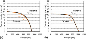
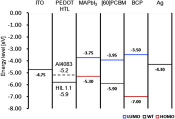
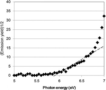
Although AI4083 is a well-known material for HTL and organic scaffolds for perovskites with an inverted structure, we used HIL 1.1 to increase the V oc of the perovskite solar cells. Figure 1 shows the I–V characteristics of MAPbI3 perovskite cells incorporating AI4083 or HIL 1.1. The PCEs of the cells were 7.0% and 8.1%, respectively. The incorporation of HIL 1.1 led to an increase in the V oc of the cells to about 1 V, which is similar to the levels of the mesoporous structure. Reference Burschka, Pellet, Moon, Humphry-Baker, Gao, Nazeeruddin and Grätzel28 Many researchers have reported smaller V oc for inverted structures consisting of AI4083 compared with mesoporous structures. Reference Lim, Kim, Jeong, Kim, Kim and Lee29,Reference Zuo, Williams, Liang, Chueh, Liao and Jen30 Figure 2 shows a schematic diagram of the energy levels of the inverted structure in this study. Values in the figure were taken from the literature. Reference Sugiyama, Ishii, Ouchi and Seki31–Reference Kim, Williams, Cho, Chueh and Jen33 Figure 3 shows the work function of HIL 1.1 as measured by PES. The work function of HIL 1.1 was higher (5.9 eV) than the valence band of the perovskite (5.3 eV). This resulted in electron transfer from the semiconductor to the PEDOT, which has been observed in previous studies using ultraviolet photoelectron spectroscopy and electron spin resonance. Reference Burschka, Pellet, Moon, Humphry-Baker, Gao, Nazeeruddin and Grätzel28,Reference Zuo, Williams, Liang, Chueh, Liao and Jen30,Reference Peisert, Knupfer, Zhang, Petr, Dunsch and Fink34–Reference Marumoto, Fujimori, Ito and Mori36 The electron transfer causes an energy-level shift in perovskite at the HIL 1.1-perovskite interface, which is related to the interfacial electric dipole layer. We conclude the energy-level shift creates an ohmic contact and decreases V oc loss at the interface. Further studies are needed to completely understand the detailed mechanism by direct observation of charge formation. We used HIL 1.1 as an organic scaffold for forming MAPb(I(1−X)Br X )3 as described in a following section.
J–V characteristics of solar cells under the AM1.5 spectrum (100 mW/cm2). (a) AI4083 was used as a PEDOT HTL. (b) HIL 1.1 was used as a PEDOT HTL. Curves were measured by forward and reverse scans. Cells had an active area of 1 cm2.

Energy diagram of ITO/PEDOT HTL/MAPbI3/PCBM/BCP/Ag. Energy values are approximate and given in eV with respect to the vacuum level. Values for the highest occupied molecular orbital or conduction band, the lowest unoccupied molecular orbital or valence band, and the work function were taken from the literature. Reference Sugiyama, Ishii, Ouchi and Seki31–Reference Kim, Williams, Cho, Chueh and Jen33

PES spectra of HIL 1.1. Spectra were taken of films on an ITO/glass substrate.

B. Substitution of Br in X site
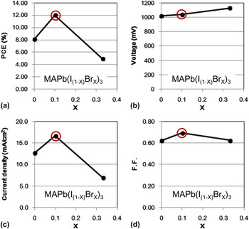
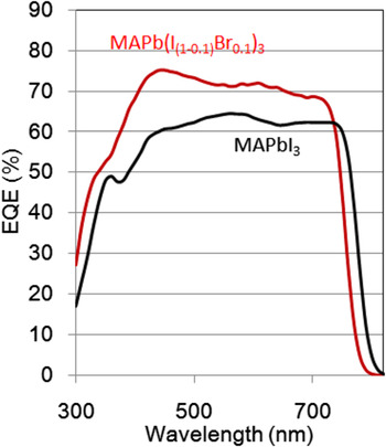
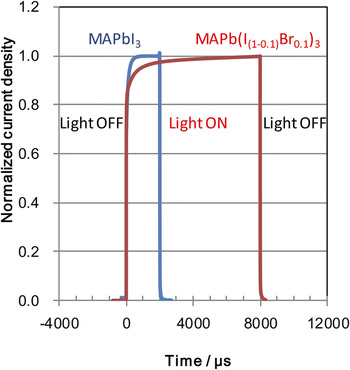
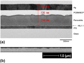
We tuned the perovskite layer via substitution of Br for I. The gas blowing method was used to form the perovskite layer in this case, as described above. Figure 4 shows the device parameters of the cells. In each graph, the X-axis is the Br composition. The PCE exhibited the highest value when X was 0.1. Although MAPbI3 (X = 0) has a wide absorption range, its J sc was lower than that of MAPb(I(1−0.1)Br0.1)3. Moreover, a low fill factor (FF) accompanied the decrease in J sc. A previous study has analyzed an ink-to-solid process during solution processing of perovskite formulations. In the cases of MAPbI3 and MAPb(I(1−X)Br X )3, the as-cast films contained ordered and disordered sol–gel precursors, respectively. Reference Munir, Sheikh, Abdelsamie, Hu, Yu, Zhao, Kim, Tall, Li and Smilgies37 It was concluded that the precursor solution of MAPb(I(1−X)Br X )3 created crystalline MAPb(I(1−X)Br X )3 and amorphous MAPbI(3−X)·DMF during solution processing, although the precursor solution of MAPbI3 creates crystals of MPAbI3·DMF and PbI2. The amorphous MAPbI(3−X)·DMF formed from MAPb(I(1−X)Br X )3 precursor solution might provide a smoother surface for the perovskite layers to regulate the rapid formation of crystals. Therefore, when X was 0.1, FF might be improved. Figure 5 shows the EQE of MAPbI3 and MAPb(I(1−0.1)Br0.1)3. Because the perovskite layer contained Br, we confirmed a lowered wave length edge. We also confirmed a relatively high EQE at absorption wavelengths. Figure 6 shows the transient photocurrent signal. Reference Shao, Xiao, Bi, Yuan and Huang38 The signal exhibited a rapid increase in current density, though the photocurrent rise to the maximum value was slower than that of MAPbI3. The slowing might be attributable to different carrier trapping rates, which increases with increasing Br content in MAPb(I(1−X)Br X )3. Reference Yang, Yang, Li, Crisp, Zhu and Beard39 The cross-sectional TEM images of the devices are shown in Fig. 7(a), from which the thickness of the perovskite layer can be observed. The perovskite layers spin-coated with gas blowing exhibited smooth surfaces. To observe a wider area, the same devices were analyzed by SEM. Cross-sectional SEM images of the perovskite layers are shown in Fig. 7(b). We confirm that the perovskite layers are formed without voids. We have reported perovskite layers spin-coated without gas blowing exhibit rough surfaces and voids in MAPbI3 on PEDOT:PSS. Here, we conclude that the gas blowing method is suitable for fabricating the perovskite layer, even though the perovskite layer contains Br. The standard deviation was ±0.2 in forward and reverse scans (see Fig. S4 in the Supplementary Material). Previous studies have reported low reproducibility of perovskite solar cells, Reference Lee, Teuscher, Miyasaka, Murakami and Snaith40 which is an important issue in industrial production. Table I summarizes representative examples with high PCE reproducibility and our results. Reference Li, Bi, Yi, Décoppet, Luo, Zakeeruddin, Hagfeldt and Grätzel10,Reference Gotanda, Mori, Matsui and Oooka13,Reference Chen, Wu, Yue, Liu, Zhang, Yang, Chen, Bi, Ashraful, Gratzel and Han41 Compared with these previous studies, our approach had a lower standard deviation, even when MAPb(I(1−X)Br X )3 was used. Antisolvent methods require quick coating above the surface of the perovskite precursor solution to form a smooth perovskite layer on the substrate. Spin-coating can be used for quick coating at the laboratory-scale. However, because there are no options available for quick coating on a large scale, the size of the active area is limited. Vacuum-flash solution processing requires a vacuum chamber to form the perovskite layer. Therefore, the size of the active area is also limited. The gas blowing method dose not requires quick coating or a vacuum chamber. The gas blowing method contributes to realizing industrial production of perovskite modules.
Cell performance versus Br content: (a) PCE, (b) V oc, (c) J sc, and (d) FF. In each graph, the X-axis shows the Br composition. Cells had an active area of 1 cm2.

EQE spectrum of the perovskite solar cell. The red line shows results for MAPb(I(1−0.1)Br0.1)3 and the black line shows results for MAPbI3. Cells had an active area of 1 cm2.

Transient photocurrent of cells prepared by gas blowing. A white LED was used as the light source for the measurement. The red line shows results for MAPb(I(1−0.1)Br0.1)3 and the blue line shows results for MAPbI3. Cells had an active area of 1 cm2.

Cross-sectional images of perovskite solar cell and perovskite layer. MAPb(I0.9Br0.1)3 spin-coated on HIL 1.1. (a) Cross-sectional TEM image, scale bar is 300 nm, and (b) cross-sectional SEM image, scale bar is 1.0 µm.

Summary of reproducibility of PCE from prior studies and this study. In all experiments, fabricated cells had an active area of 1 cm2.

IV. CONCLUSIONS
The gas blowing method was used to create a flat perovskite layer with reduced defects at the PEDOT/perovskite interface and with a 1 cm2 active area even with a mixed halide perovskite. Incorporation of PEDOT HTL with a higher work function was found to increase the V oc of inverted structure solar cells. All layers of the cells were fabricated at temperatures below 140 °C. Low temperature processes for fabricating solar cells are important for incorporating polymer substrates to create flexible solar cells and high-throughput fabrication in the future. The standard deviation of PCE was found to be ±0.2 in forward and reverse scans, which is useful for industrial production. Our findings are expected to contribute to the industrial production of perovskite solar cells.
Supplementary Material
To view supplementary material for this article, please visit https://doi.org/10.1557/jmr.2017.264.
ACKNOWLEDGMENT
We gratefully acknowledge funding from the New Energy and Industrial Technology Development Organization (NEDO) through a project for perovskite solar cells.