Modern material fabrication platforms enable production of a wide class of composites with ever more complex internal structures. Recently, plasmonic nanowire and nanolayer-based material assemblies have emerged as platforms of choice for modulating the diffraction limit and local density of photonic states,[ Reference Krishnamoorthy, Jacob, Narimanov, Kretzschmar and Menon 1 – Reference Cortes, Newman, Molesky and Jacob 3 ] opening potential applications in sensing, microscopy, and quantum optics.[ Reference Wells, Zayats and Podolskiy 4 – Reference Poddubny, Iorsh, Belov and Kivshar 9 ] In related but separate efforts, techniques for nanowire growth and nanolayer deposition have been perfected by the semiconductor research community. In this context, semiconductor nanowires have emerged as a promising platform for high-performance light-emitting devices, where InGaN nanowire light-emitting diodes (LEDs) have shown superior performance compared with their bulk counterparts.[ Reference Kuykendall, Ulrich, Aloni and Yang 10 – Reference Fickenscher, Shi, Jackson, Smith, Yarrison-Rice, Zheng, Miller, Etheridge, Wong, Gao and Deshpande 15 ] There is still lack of development of high-performance nanowire lasers due to the inherent challenges to incorporate high-quality reflector mirrors to form low-loss laser cavities.[ Reference Qian, Li, Gradečak, Park, Dong, Ding, Wang and Lieber 16 – Reference Arafin, Liu and Mi 18 ] One possible candidate for such reflectors is AlN/GaN-distributed Bragg reflector (DBR) heterostructures, which can be directly implemented within the existing material fabrication framework. However, owing to the complexity of the nanowire heterostructures, the simple transfer-matrix method (TMM)[ Reference Rytov 19 , Reference Yeh, Yariv and Hong 20 ] cannot be applied directly as in the case of bulk DBR structure design, and full three-dimensional (3D) solvers have to be used to design and characterize optical performance of nanowire-based DBRs.[ Reference Heo, Zhou, Guo, Ooi and Bhattacharya 21 ] Here we demonstrate that optical properties of nanowire/nanolayer arrays can be adequately described by effective-medium theories (EMTs), significantly reducing computational effort required for the analysis and optimization of epitaxial DBRs.
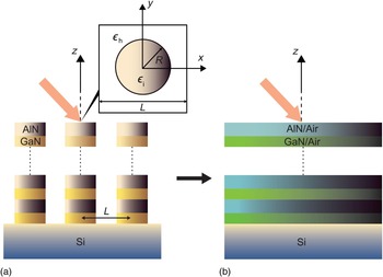
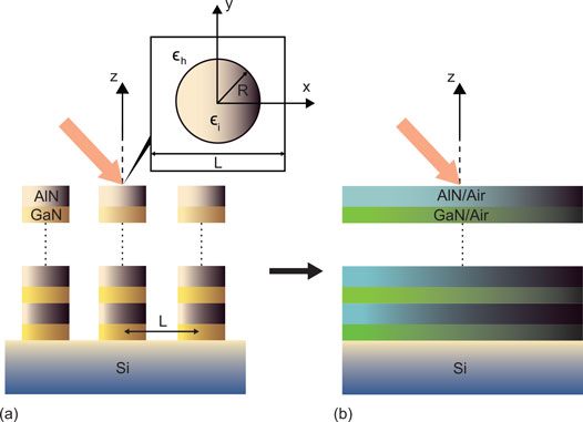
EMT presented in this work is a convenient numerical extension to the well-known Maxwell–Garnett (MG) formalism[ Reference Maxwell Garnett 22 ] in the limit of high inclusion concentration. As such, the developed technique can be used as an alternative to previously developed analytical techniques[ Reference Wells, Zayats and Podolskiy 4 , Reference Perrins, McKenzie and McPhedran 23 – Reference Godin 28 ] that are valid in the limit of few-multipole response of nanowire media. The main motivation to undertake this project lies in the analysis of optical response of semiconductor nanowire arrays, similar to ones presented in Ref. Reference Heo, Zhou, Guo, Ooi and Bhattacharya21 [see Fig. 1(a)] and other complex composites with similar internal structure. Here, we use the examples of plasmonic nanowire arrays as well as of heterostructures that comprise arrays of aligned dielectric nanowires with radius of r = 50 nm, and interwire separation, L = 105 nm. Each wire, in turn consists of an array of 20 AlN/GaN layer pairs, with 77 nm-thick AlN layers and 71 nm-thick GaN layers. The space between the wires is empty. The structure as a whole is fabricated on top of an Si substrate [see Fig. 1(a)], and operates in the visible-frequency regime.
(a) Schematic representation of array and unit cell of AlN/GaN nanowire Bragg mirror. The thickness of the AlN/GaN layers are 77 and 71 nm, respectively. (b) Visualization of the homogenization procedure used to represent the heterostructures of DBR consisting of GaN/air and AlN/air composite materials for the constituent layers.

In the derivation of effective-medium response, we assume that both the lattice size and wire radius are much smaller than the operating wavelength, while we do not impose significant constraints on the thickness of individual layers within the nanowire. As a result, we utilize EMT to deduce (anisotropic) effective-medium parameters for each individual sublayer of wire medium [Fig. 1(b)], and then use transfer-matrix formalism[ Reference Rytov 19 , Reference Yeh, Yariv and Hong 20 ] to calculate the overall optical response of the metamaterial. Accuracy of effective-medium description is verified by numerical solutions of Maxwell equations with commercial finite-element solvers.[ 29 ] Interestingly, as we show in this work, the developed formalism works rather well even when the layer thickness is comparable with radius.
This presented approach can be used to design complex photonic devices based on both plasmonic and all-dielectric nanowire media, with nanowires arranged in square or rectangular unit cells. Extension of the presented formalism to hexagonal unit cell will be presented elsewhere. Previous studies[ Reference Elser, Wangberg, Podolskiy and Narimanov 25 , Reference Rayleigh 26 ] indicate that the exact shape of the unit cell does not significantly affect the EMT response of the composite, which is primarily governed by the wire concentration and (for anisotropic composites), by mean wire cross-section and mean wire–wire separation. The rest of the paper is arranged as follows. In Section 2, we outline the derivation of effective-medium formalism for nanowire materials and analyze the implication of the shape of the unit cell and component filling fraction on the validity of the EMT. In Section 3, we use the developed framework, in combination with transfer matrix approach, to analyze photonic band gap behavior in nanowire composites with layered internal structures. Finally, Section 4 concludes the paper.
Effective-medium response of the wire media
Electromagnetic properties of composites have been a topic of active research for over a century[
Reference Maxwell Garnett
22
–
Reference Milton
27
] dating back, at least, to attempts of J.C. Maxwell Garnett to analyze the colors in metal glasses and in metallic films. The resulting MG EMT can successfully describe the optical response of materials where subwavelength spheroidal inclusions are dispersed in a homogeneous host. The original MG approach assumes spheroids are homogeneously distributed over the host material, and are substantially diluted, so that a field scattered by each inclusion can be approximated by the field of a point dipole positioned at the site of the inclusion. In the case of composites consisting of aligned wires (radius r ≪ λ, permittivity ε
i
) with circular cross-section aligned into isotropic (square) lattice with wire–wire separation L ≪ λ inside the host material (permittivity ε
h) [see Fig. 1 (insert)], the resulting effective permittivity is described by a (diagonal) tensor with components ε
x
= ε
y
= ε
⊥; ε
z
≠ ε
⊥ (here we assume that
 $\hat z$
represents the direction of the wire axis), with
 $$\epsilon _z^{{\rm mg}} = p{\epsilon _i} + (1 - p){\epsilon _{\rm h}},$$
 $$\epsilon _ \bot ^{{\rm mg}} = \displaystyle{{2p{\epsilon _i}{\epsilon _{\rm h}} + (1 - p){\epsilon _{\rm h}}({\epsilon _i} + {\epsilon _{\rm h}})\;} \over {2p{\epsilon _{\rm h}} + (1 - p)({\epsilon _i} + {\epsilon _{\rm h}})}},$$
where p = πr
2/L
2 represents the concentration of wire inclusions inside the host material. MG formalism has been successful in describing optical properties of wire media in the limit where
 $p{\rm\,\lesssim}\, 0.3$
, and has been generalized to describe the properties of dilute wire media with wires having elliptical cross-sections, arranged into an anisotropic lattice.[
Reference Elser, Wangberg, Podolskiy and Narimanov
25
] For higher concentration of inclusions, the dipole approximation fails and higher-order multipoles need to be considered.[
Reference Perrins, McKenzie and McPhedran
23
,
Reference Meredith and Tobias
24
,
Reference Rayleigh
26
] The exact number of multipoles that need to be included for proper treatment of effective-medium response strongly depends on the concentration and permittivity of wires (see Ref. Reference Perrins, McKenzie and McPhedran23 for dielectric wires and Fig. 4 for plasmonic media).
The approach that allows analytical solutions of EMT with arbitrary precision was originally outlined by Lord Rayleigh,[ Reference Rayleigh 26 ] and was subsequently corrected in Refs Reference Perrins, McKenzie and McPhedran23, Reference Meredith and Tobias24. Unfortunately, an analytical description of EMT requires numerical summation of weakly converging sums, and becomes increasingly untrackable for multipoles over 7 (accuracy that is required for plasmonic and high-concentration wire composites). Here we present a modification of EMT approach that naturally lands itself on numerical linear algebra solvers that are widely available today. As an added benefit, our technique can treat composites with multi-shelled wire inclusions arranged into anisotropic (rectangular) lattice, and can be further extended to treat wires with non-circular cross-sections and to wires arranged into hexagonal and other lattice shapes.
The goal of any EMT is to relate the permittivity of the components of the composite, the geometrical parameters, and the effective-medium response (here, ε
⊥, ε
z
). Similar to previous EMT treatments, we use a quasi-static approximation to find the (microscopic) distribution of electric field within the (subwavelength) unit cell
 $\vec E(x,y)$
(see Fig. 2), which can then be used to calculate effective permittivity as a result of averaging
 $$ \langle \epsilon {\rm (}x,y{\rm )}\; {E_\alpha} (x,y)\rangle = {\epsilon _{\alpha \beta}} \langle {E_\beta} (x,y)\rangle .$$
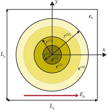
Schematic representation of rectangular unit-cell geometry for cylindrical shells used to build EMT.

Geometry of a unit cell considered in this work is shown in Figs. 1 and 2. Boundary conditions require continuity of the z-component of the electric field along the unit cell. Therefore, in the quasi-static approximation, similar to previous studies, we find
 $${\epsilon _z} = \displaystyle{ \langle {\epsilon {E_z \rangle}} \over { \langle {E_z}\! \rangle}} = \, \langle \epsilon (x,y) \rangle .$$
To calculate an electric-field distribution in the xy-plane, we assume that the external electric field is applied to the composite in the x-direction, and relate the field inside each cylindrical shell [layer (l)] (Fig. 2) to the potential
 $${E^{(l)}} = - \vec \nabla {U^{(l)}}.$$
The electric potential, in turn, is given by
 $$\eqalign{{U^{(l)}}(r,\phi ) & = a_0^{(l)} + \mathop \sum \limits_{m = 1}^\infty \left( {a_m^{(l) +} {r^m} + a_m^{(l) -} \displaystyle{1 \over {{r^m}}}} \right)\cos {\kern 1pt} (m\phi ) \cr & \quad + b_0^{(l)} \ln (r) + \mathop \sum \limits_{m = 1}^\infty \left( {b_m^{(l) +} {r^m} + b_m^{(l) -} \displaystyle{1 \over {{r^m}\;}}} \right)\sin (m\phi ).} $$
In the expressions above, index l represents the layer number (see Fig. 2), while index m corresponds to multipole order. Due to symmetry considerations, all
 $b_m^{(l) +} = b_m^{(l) -} = 0$
, as well as
 $a_{2n}^{(l) +} = a_{2n}^{(l) -} = 0$
.
Note that in the outer-most layer
 $a_1^{(N) -} = 1$
, representing the homogeneous excitation field. The problem of building the EMT is essentially equivalent to the calculation of all remaining coefficients in Eq. (6). Applying boundary conditions at each cylindrical interface, yields a linear relationship between the coefficients in the neighboring layers, as well as between coefficients
 $a_m^{(l) +} $
and
 $a_m^{(l) -} $
within the same layer; for wires with circular cross-sections these relationships can be represented by diagonal matrices S
(l) and T
(l):
 $$S_m^{(l)} a_m^{(l) +} = a_m^{(l) -} ;\quad T_m^{(l)} a_m^{(l + 1) +} = a_m^{(l) +}, $$
where S (1) is a zero matrix, and the remaining matrices are constructed using the following recursive relations:
 $$T_m^{(l)} = \displaystyle{{2{\epsilon ^{(l + 1)}}} \over {{\epsilon ^{(l + 1)}}}} + \displaystyle{{S_m^{(l)} \left( {{\epsilon ^{(l + 1)}} - {\epsilon ^{(l)}}} \right)} \over {{r^{{{(l)}^{2m}}}}}},$$
 $$S_m^{(l + 1)} = S_m^{(l)} T_m^{(l)} + \left( {T_m^{(l)} - 1} \right){r^{{{(l)}^{2m}}}}.$$
Analytical techniques previously presented in Refs. Reference Perrins, McKenzie and McPhedran23, Reference Meredith and Tobias24 aimed to find for self-consistent solutions where the field incident on a given inclusion resulted from a superposition of external fields and multipole fields scattered by all other inclusions. The latter part yields a set of sums, some of which (such as the sum over dipole contributions within a layer) converge rather weakly,[ Reference Perrins, McKenzie and McPhedran 23 ] making the resulting analytical expressions to become increasingly cumbersome for higher order (larger m) EMTs.
Equivalently, the same solution can be found by analyzing the individual unit cell of the metamaterial and a set of boundary conditions that would mimic the effects of all other cells of the composite. For wire composites with rectangular cells (Fig. 2) such boundary condition can be written as
 $${\left. {{E_y}} \right \vert _{\rm \Gamma}} = 0$$
with Γ being the unit-cell boundary. This boundary condition, while inconvenient for analytical calculations, is easily implemented into numerical linear algebra packages. In this work, we enforce Eq. (10) along the x = (L
x
/2), y ∈ [0, (L
y
/2)], and x ∈ [0, (L
x
/2)], y = (L
y
/2) parts of the boundary. Equation (10) is automatically satisfied across the remaining boundary due to symmetry of the solution. In our Matlab-based implementation (http://viktor-podolskiy-research.wiki.uml.edu/Effective+medium+theory+for+nanowire+composites) Eq. (10) is used, in combination with Eqs. (5)–(9) to find the set of coefficients
 $a_m^{(l) \pm} $
based on
 $a_1^{(N) -} = 1$
; the overdetermined problem (number of {x, y} points used is larger than the number of unknown coefficients) is automatically treated by linear solvers as least-squares optimization problem, producing in our tests, converging solutions that do not depend on the (sufficiently large) number or position of points along the boundary.
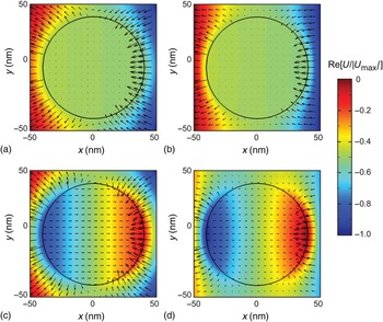
The potential and field profiles produced by dipole-based and multipole-based EMTs are shown in Fig. 3. It is seen that in high-concentration wire arrays multipole contributions provide significant corrections to MG EMT.
EMT calculations of potential and electric fields in the unit cell where surface plots and arrows represent Re[U/|U max|] and Re[E x,y ] components, respectively. (a, b) p = 0.5 and ε i = 50 + 0.1i in air (a) is dipole-based and (b) multipole EMTs. (c, d) p = 0.5 and ε i = −5 + 0.1i in air (c) is dipole-based, and (d) multipole EMTs.

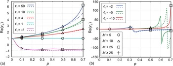
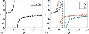
As the wire permittivity or wire concentration increases, larger numbers of multipoles are required to obtain convergent solutions. The number of multipoles [the number of terms in Eq. (6)] required to obtain convergent EMT prediction, depends on combination of wire permittivity and concentration, as seen in Fig. 4. For dielectric wires, the number of required multipoles monotonically increases with increase of wire permittivity or concentration. In this limit, results of our numerical calculations agree with previously published results.[ Reference Perrins, McKenzie and McPhedran 23 ] For plasmonic wires, number of required multipoles also rapidly increases in the vicinity to MG resonance, collective excitation of plasmons corresponding to charge-density oscillations perpendicular to wires.
(a, b) Comparison of dipole-based (dashed lines) and multipole (solid lines) EMTs for predicting effective-medium response of nanowire arrays for varying fill fraction p and wire permittivity ε i with Im(ε i ) = 0.1 in air for a square unit cell. The symbols corresponded to the multipole convergence M. Panel (b) illustrates the plasmonic regime.

Figure 5 summarizes the performance of the developed numerical technique for plasmonic wires arranged into rectangular unit cell. It is seen that the predictions of the EMT developed here agree with direct numerical solutions of Maxwell equations, previously reported in Ref. Reference Elser, Wangberg, Podolskiy and Narimanov25. It is also seen that higher multipoles yield significant improvement of the EMT with respect to previously developed dipole-based analytical technique.
Comparison of dipole-based (dashed lines) and multipole (solid lines) EMTs for predicting effective-medium response of plasmonic nanowire arrays (ε in = −2.5, ε h = 2) arranged in square (a) and rectangular (b), L x = 1.1; L y = 1/1.1 lattices; symbols represent the results of numerical solutions of Laplace equation, as described in Ref. Reference Elser, Wangberg, Podolskiy and Narimanov25.

Photonic band gap structures based on nanowire arrays
We now consider the optical properties of layered wire composites, schematically shown in Fig. 1. The procedure to calculate optical response of these composites is a two-stage process. In the first stage, each layer of the multilayered composite is considered separately, and is replaced by its homogeneous effective-medium analog [Fig. 1(b)], with effective-medium permittivity calculated using the EMT described above. In the second stage, the optical properties of the resultant multilayer structure are calculated. Here we utilize the well-developed TMM[ Reference Rytov 19 , Reference Yeh, Yariv and Hong 20 ] to perform these calculations.
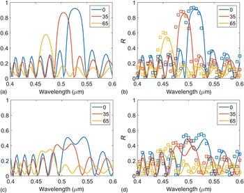
The goal of this project is to assess test the applicability of EMT/TMM combination to describe the optical response of multilayer stacks of GaN/AlN and AlN/GaN multilayers in the limit of relatively thin layers. As seen in Fig. 6, the EMT/TMM combination provides adequate quantitative prediction of the optical response of the nanowire/nanolayer composites, as compared with full-wave numerical solutions of Maxwell equations using 3D finite-element-method (FEM) solver. In fact, an effective-medium technique is able to describe both amplitude of the reflectance as well as the spectral shifts of DBR maxima in response to angle of incidence. The minor spectral shift between EMT and FEM predictions is due to the combination of the geometrical constraints that push EMT to its limits. Indeed, the structure under consideration has: (i) the layer thickness that is comparable with wire diameter, as well as (ii) unit cell that is only one-third of the internal wavelength (at λ = 500 nm). For the structure considered in this work, the latter issue represents the main limitation to accuracy of the EMT formalism. Indeed, when the unit-cell geometry is reduced in half (L = 50.5 nm, r = 25 nm, the results of FEM and EMT calculations are almost super-imposable despite the fact that the layer thickness is still comparable with wire diameter.
Solid lines: reflectivity spectra of AlN–GaN–nanowire-based DBR structures calculated using the direct FEM numerical solution of Maxwell equations (a, c) and using EMT (b, d). In all cases, the structure contains 20 bi-layers of AlN and GaN deposited on the Si substrate; panels (a, c) represent the case when the AlN/GaN layer is deposited first; panels (b, d) correspond to GaN/AlN adjacent to the substrate. Symbols in (b, d) represent FEM solutions for the system where the unit-cell geometry was reduced by a factor of 2, moving the structure closer to validity of EMT.

Conclusions
To conclude, we presented a numerical technique that can be used to extend MG EMT for nanowire composites in the limit where the wire inclusions have high filling fractions positioned in anisotropic unit cells. This numerical approach can easily be implemented using commonly available numerical linear algebra solvers. Matlab implementation has been developed and tested. The formalism was verified on metamaterial formed by plasmonic wires arranged in rectangular unit cells. In a separate set of tests, the formalism was used in combination with the transfer-matrix technique to describe photonic band gap behavior observed in nanowires containing AlN/GaN DBR heterostructures. Results of both studies were tested against full-wave numerical solutions of Maxwell equations and the agreement between the two solutions was demonstrated.
The EMT, presented here for nanowire composites with circular wires arranged into rectangular unit cells can be straightforwardly extended to other unit cell geometries as well as to non-circular wires. The EMT and its numerical implementation presented in this work has potential to drastically reduce the computational efforts in design and analysis of wire-based heterostructures as compared with full-wave 3D numerical solvers thus significantly reducing computational effort required for analysis and optimization of DBR and other photonic components based on nanowire composites. The formalism can be also used to extend the nonlocal description of wire metamaterials[ Reference Wells, Zayats and Podolskiy 4 ] to the limit of high-wire concentration.
Acknowledgment
This work was partially supported by the US Army research office (Grant no. W911NF-12-1-0533).